Accepted Manuscript
Full Length ArticleA detailed study on the Fe-doped TiO2 thin films induced by pulsed laser dep-osition route
Lijian Meng, Zhenhua Wang, Liang Yang, Weijun Ren, Wei Liu, Zhidong Zhang, Tao Yang, M.P. dos Santos
PII: S0169-4332(18)30703-7
DOI: https://doi.org/10.1016/j.apsusc.2018.03.043
Reference: APSUSC 38791
To appear in: Applied Surface Science Received Date: 2 November 2017 Revised Date: 26 February 2018 Accepted Date: 5 March 2018
Please cite this article as: L. Meng, Z. Wang, L. Yang, W. Ren, W. Liu, Z. Zhang, T. Yang, M.P. dos Santos, A detailed study on the Fe-doped TiO2 thin films induced by pulsed laser deposition route, Applied Surface Science (2018), doi: https://doi.org/10.1016/j.apsusc.2018.03.043
This is a PDF file of an unedited manuscript that has been accepted for publication. As a service to our customers we are providing this early version of the manuscript. The manuscript will undergo copyediting, typesetting, and review of the resulting proof before it is published in its final form. Please note that during the production process errors may be discovered which could affect the content, and all legal disclaimers that apply to the journal pertain.
A Detailed Study on the Fe-doped TiO2 Thin Films Induced by Pulsed Laser
Deposition Route
Lijian Menga,c) , Zhenhua Wangb), Liang Yangb), Weijun Renb), Wei Liub), Zhidong
Zhangb), Tao Yangd,e) *and M. P. dos Santosf)
a) Functional Materials Laboratory, School of Materials & Mineral Resources, Xi’an University of Architecture and Technology, China
b) Shenyang National Laboratory for Material Science, Institute of Metal Research, Chinese Academy of Sciences, China.
c) Departamento de Física and Centre of Innovation in Engineering and Industrial Technology, Instituto Superior de Engenharia do Porto, Instituto Politécnico do Porto, Portugal.
d) Key Laboratory of Biofuels, Qingdao Institute of Bioenergy and Bioprocess Technology, Chinese Academy of Sciences, China
e) TEMA, Department of Mechanical Engineering, University of Aveiro, Portugal
f) CEFITEC, Universidade Nova de Lisboa/Departamento de Física, Universidade de Évora, Portugal
Abstract
Fe-doped TiO2 thin films are deposited both on the (100) oriented Si and glass
substrates by pulsed laser deposition technique using Fe powder doped TiO2 ceramic
target. The structural and optical properties of the film have been studied in detail. The degree of film crystallinity is investigated by X-ray diffraction and confirmed by Raman scattering measurements. The stoichiometry and chemical states of Fe, Ti and O are probed by X-ray photoelectron spectroscopy. The surface morphologies are observed by Scanning electron microscopy. The optical properties are studied by measuring the transmittance and the optical constants, the refractive index and the extinction coefficient. It is found that the substrate temperature is a key factor in determining the thin film structure which further influences the refractive index and the optical band gap of the film. An anatase structure emerges above 300 ºC while the rutile structure appears when the substrate temperature is higher than 500 ºC. Another result is that Fe
exists in the deposited films as Fe3+ and the atomic concentration of Fe in the films is
much lower than that in the source target.
Keywords: Fe-doped TiO2, Structural Properties, Optical Properties; PLD, Thin Film
1. Introduction
Recently, the transition metal-doped TiO2 films have been studied extensively due to
their promising applications in the fields of photocatalysis and dilute magnetic semiconductors (DMS)[1, 2]. Because of its relatively high catalytic activity, robust
chemical stability, low cost and non-toxicity, TiO2 itself has been used as a
photocatalyst in water and air remediations. TiO2 is also used in the dilute magnetic
semiconductor (DMS) area. DMS are essential materials for the development of “spintronic” devices, which simultaneously utilize the charge and spin of the carriers.
However, in both scenarios, TiO2 has to be modified or doped to function well because
it is active only under near-ultraviolet irradiation due to its wide band gap energy. The principal objective of doping with transition metal is to narrow the optical band gap of
TiO2 and make it active under visible-light irradiation. By doping with transition metal
ions into cation sites in the host semiconductor lattice (such as TiO2 and ZnO),
ferromagnetic properties are introduced into nonmagnetic semiconductors [3, 4]. Doping may modify the structural and optical properties of the host materials. Therefore, it is necessary to make a detailed study on these properties after doping for the possible applications in the mentioned areas.
Pulsed laser deposition technique has become a widely used physical technique for depositing films because it has many advantages, such as a wide choice of materials, high instantaneous deposition rate, and a relatively high reproducibility. In addition, this technique has several unique features: a fine control on stoichiometry, the possibility to use thermally sensitive substrates and the capability to grow nanostructures and cluster-assembled films by ablating material in presence of a background gas. Some works
have been reported on Fe-doped TiO2 films prepared by pulsed laser deposition.
However, most of the studies are focused on the magnetic properties of the synthesized films, less attention has been paid to the structural properties[5, 6]. In these works, only XRD results were mentioned for structural studies. Although the magnetic properties
are very important for Fe doped TiO2 films, more systematic fundamental research on
the structural and optical properties should be conducted to get a deeper understanding of the magnetic coupling in these novel electronic materials. In this work, the structural and optical properties of the films deposited on (100) oriented Si substrates by pulsed
laser deposition have been reported. Unlike the former studies, Fe-doped TiO2 ceramic
target source has been used and special attention is paid on the temperature of the substrate in determining the structure of the films which further influences the refractive index and the optical band gap of the films.
2. Experimental details
2.1 Characterization
X-ray diffraction (XRD) was performed using a Rigaku RINT2000 diffractometer. The X-ray photoelectron spectra (XPS) were measured by a VG ESCALAB250 electron analyzer using a monochromatic Al Kα source operating at 150 W (10 mA, 15 kV), micro-focused to a spot size of 500 µm. High-resolution spectra were collected with 50 eV pass energy and 0.1 eV step energy. The number of the scan is 10 for acquiring Fe spectra and is 3 for acquiring Ti and O spectra. The surface morphology of the deposited films was observed by scanning electron microscopy (SEM) (FEI, Inspect F50). The optical transmittance spectra of the films were recorded using UV/VIS/NIR spectrometer (Cary 5000, Varian, Inc.). Raman scattering measurements were performed using a semiconductor laser and a 532 nm laser line was used as the exciting light source. The laser line was focused on the sample surface in a strict 180º backscattering geometry.
2.2 Film fabrication
A pulsed KrF excimer laser (Lambda Physik LPx 305i, 248 nm, 25 ns, frequency 4 Hz)
was used to ablate the Fe-doped TiO2 ceramic target. The laser beam was focused to the
target surface by lens at a 45 degree incident angle. The Fe-doped TiO2 target with 15%
atomic percent of Fe (15 at % Fe) and a purity of 99.95% was supplied by China
Material Technology Co., Ltd. The Fe is doped in TiO2 as Fe atoms. The target was
made by vacuum hot pressing sintering process at 700 ºC. The particle size of TiO2
powder is about 1 µm and the particle size of Fe powder is between 3 to 8 µm. The laser was operated with an energy of about 500 mJ/pulse and was focused on the target to a
spot area of 1 x 8 mm2, thus producing a laser fluence of about 0.06 J/mm2. The target
was fixed at a 40 mm distance apart from the substrate. The p-type (100) oriented silicon wafers and glass slides were used as the substrates and the substrate temperature was varied from room temperature (RT) to 700 ºC. The silicon and glass substrates were ultrasonically cleaned subsequently using ethanol and de-ionized water for 5 min, and
then dried in flowing N2 gas before being loaded into the deposition chamber. The
chamber is equipped with a turbo molecular pump backed with a mechanical pump.
Before the deposition starts, the chamber was pumped down to less than 3 x 10⁻³ Pa.
After that, the oxygen gas was introduced into the chamber and the pressure was kept at 5 Pa. The deposition time was kept at 60 min for all the depositions. The thickness of the film is about 400 nm which is obtained by fitting the transmittance.
3. Results and discussion
3.1 XRD Characterization of the film
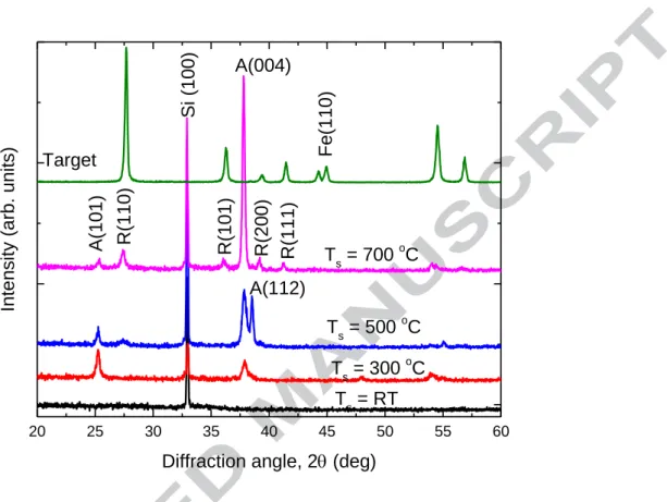
Figure 1 shows XRD patterns of Fe-doped TiO2 films prepared at different substrate
temperatures. For reference, the XRD pattern of the Fe-doped TiO2 ceramic target (15
at % Fe) is also shown in this figure. It can be seen that the target has a rutile structure (PDF card 21-1276). The (110) diffraction peak of Fe (PDF card 6-696) can also be observed in the XRD pattern of the target. It indicates that Fe exists in the target as Fe atom. The film prepared at room temperature does not show any XRD diffraction peak
from TiO2. The peak located at 33º comes from the Si substrate. The film prepared at
300 ºC substrate temperature shows an anatase phase with a preferred orientation along the [004] direction (PDF card 21-1272). As the substrate temperature was increased from 300 ºC to 700 ºC, this preferred orientation has been enhanced. The peak intensity
ratio of IA(004)/IA(101) increases from 0.94 to 24.48 as the substrate temperature is
increased from 300 ºC to 700 ºC. The XRD diffraction’s results are listed in Table 1. When the substrate temperature is higher than 500 ºC, the rutile phase appears. The
intensity of the (110) diffraction peak from rutile TiO2 increases as the substrate
temperature is increased further. It means that the component of the rutile phase increases with the substrate temperature although the anatase phase still dominates the
structure. The peak intensity ratio of the (110) peak from the rutile TiO2 and the (101)
IR(110)/IA(101) increases from 0.72 to 3.67 as the temperature is increased from 500 ºC
to 700 ºC. The average particle sizes calculated from the Scherrer equation based on the diffraction peaks are also listed in table 1. As the substrate temperature is increased, the average particle size along the anatase [101] direction decreases and those along the anatase [004] and the rutile [110] directions are increased. It means that the growths of the grains along the anatase [004] and the rutile [110] directions are enhanced as the temperature is increased. Although the target has the pure rutile phase, the deposited films are still dominated by anatase phase when the substrate temperature is higher than 300 ºC.
3.2 Raman scattering measurement
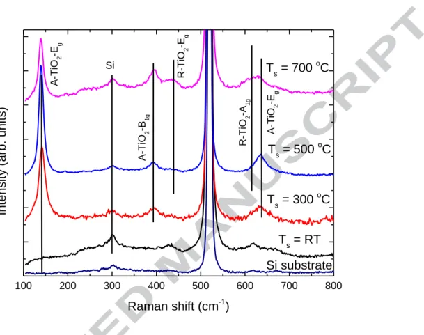
Figure 2 compares the Raman spectra of Fe-doped TiO2 films prepared at different
substrate temperatures and a silicon substrate. The film prepared at room temperature
only shows the Raman peaks from the Si substrate, and no Raman peaks from TiO2 can
be observed because of its amorphous structure. Three anatase Raman peaks, located at
142 cm-1, Eg; 400 cm-1, B1g and 641 cm-1, Eg, can be observed for the film prepared at
300 ºC substrate temperature. The anatase A1g+B1g vibration mode, which is located at
517 cm-1 is overlapped by a strong Si Raman peak. Two very weak rutile Raman peaks,
located at 446 cm-1, Eg and 612 cm-1, A1g, can be observed for the film prepared at 500
ºC substrate temperature. The intensity of these rutile Raman peaks shows a very clear increase as the substrate temperature is increased to 700 ºC, which indicates an increase of the portion of rutile phase. These results are in good accordance with the XRD measurements.
3.3 Morphology evolution with the increase of temperature
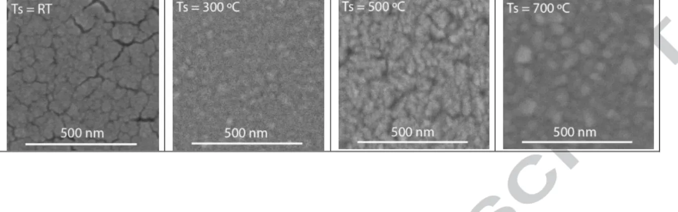
The morphology of the Fe-doped TiO2 films prepared at different substrate
temperatures are shown in Figure 3 (the magnification factors are 160000X for these images). The film prepared at room temperature has a rough surface with many small cracks. The reason which causes these small cracks is still not very clear. It may result from the residual stress in the deposited film. The films prepared at 300 ºC, 500 ºC and 700 ºC show in the surface small round-shaped grains, column-shaped grains and irregular-shaped grains, respectively. It can be seen that the grain size in the sample surface is much bigger for the film prepared at 700 ºC than for that prepared at 300 ºC. The high substrate temperature is favorable for the grain growth.
3.4 Detailed analysis on the binding energies of the Fe, Ti and O elements
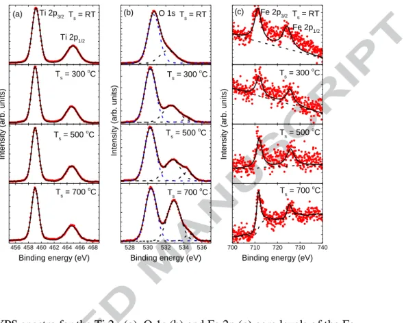
Figure 4 shows the XPS spectra of Ti 2p, O 1s and Fe 2p core levels for the Fe-doped
TiO2 films prepared at different substrate temperatures. The atomic concentrations of
the elements are calculated from measured peak areas (Ti 2p3/2, O 1s and Fe 2p3/2) with
the Scofield’s relative sensitivity factors [7] which are suitable for our XPS measurement conditions: Ti, 5.22; O, 2.93; Fe, 10.82. A standard Shirley background subtraction and Gaussian peak deconvolutions are performed for Ti 2p, O 1s and Fe 2p photoelectron spectra. All the peak positions are calibrated by taking the C 1s peak (284.6 eV) as a reference. The fitting results are summarized in Table 2. The atomic concentration of the Fe atom in the target is 15 at%. However, the atomic concentration of the Fe atom in the film is much lower (less than 1 at% as shown in table 2) than it in the target. It is still not clear why the concentrations have a so large difference. It
suggests a low ablation yield of the Fe atom compared to the TiO2 compound and
results in this low atomic concentration of Fe in the films. Further studies are necessary for making it clearly. It can be seen from table 2 that the atomic concentration of Fe in the films is slightly different for the samples prepared at different substrate temperatures. However, it must be mentioned that these values may have some errors as the intensities of the Fe 2p peak for the samples are very weak and the fittings were performed with some empirical evidences. Therefore, these values may not represent true values, but
represent a very low-level Fe doping concentration in these TiO2 films. The binding
energies of the Fe 2p3/2 are 706.9 eV, 709.9 eV and 710.8 eV for Fe atom, Fe2+ ion in
FeO and Fe3+ ion in Fe2O3 respectively [8, 9]. From Fig. 4 it can be seen that the
binding energies of the Fe 2p3/2 for the Fe-doped TiO2 films prepared at different
substrate temperatures are close to the value of 710.7 eV. It means that the Fe exists in
all films as Fe2O3 compounds although it exists in the target as Fe atoms. It also
suggests that Fe atoms have been fully oxidized as no Fe2+ ions are detected in the films.
The Fe atoms may get oxidized when they travel from the target to the substrate as the chamber is filled with oxygen gas. In addition, these Fe atoms are easily get fully oxidized as the number of the Fe atom removed from target is very low and results in
the formation of the Fe2O3. It can be seen from Fig. 4(a) that the XPS spectra of Ti 2p
core level, from the films prepared at different substrate temperatures, have the good
symmetries and the binding energies are very close to the value of Ti4+ ion from TiO2
oxidation states (such as Ti3+, Ti2+) related to the oxygen deficiencies in TiO2 lattice
exist in the films, indicating a fully oxidation for all the films. The Ti 2p binding energy shows an energy shift to lower energy as the substrate temperature is increased. This energy shift does not result from the variation of the valence state of titanium as it
has been discussed that the titanium has the same valence states (Ti4+) in all the films.
Since a similar shift for the O 1s binding energy is also observed for the films prepared at different substrate temperatures, these energy shifts can be attributed to the shift of
the Fermi level of TiO2 [10]. By deconvolution of O 1s core level spectra, three peaks,
located approximately at 529 eV, 531 eV and 533 eV can be observed, except for the film prepared at room temperature, in which only two peaks located approximately at 529 eV and 531 eV can be observed. The peak located approximately at 529 eV is
attributed to signal of oxygen ionic state (O2-) in TiO2 lattice. The peaks located
approximately at 531 eV and 533 eV are attributed to hydroxide or hydroxyl groups
(OH-) and hydrate and/or adsorbed water (H2O) [11, 12]. The OH- groups may be
formed by the interaction of hydrogen with surface oxygen ions or by the interaction of water with metal ions at the surface. The surface contamination and adsorption of water have also the contributions to them. The change in the binding energy of OI, OII and OIII observed at different substrate temperatures which are attributed to the change in
the physical properties [13] of the Fe doped TiO2. These results are also consistent with
those shown in table 1. The O/Ti ratio has been calculated using O2- component for all
the films and the results are given in Table 2. It can be seen that the values are equal or over than 2 meaning that the films are fully oxidized.
3.5 Optical Properties of the Fe-doped TiO2 films
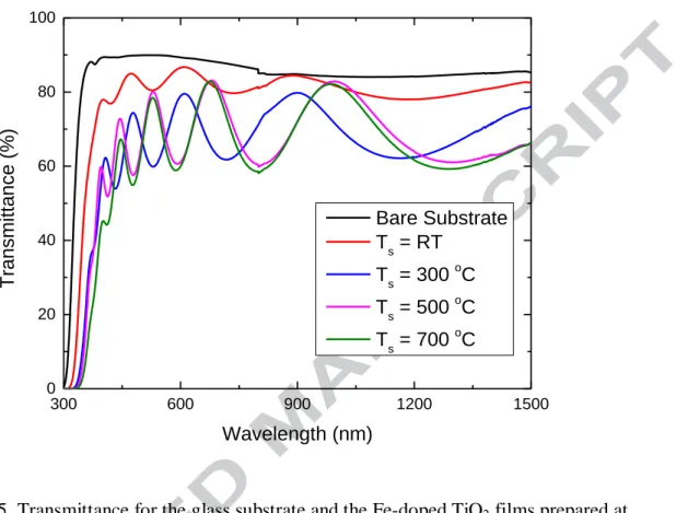
Figure 5 shows the transmittance of the Fe-doped TiO2 films deposited at different
substrate temperatures. For comparison, the transmittance of the glass substrate without film is also shown in the figure. Generally, the glass will get soften but still maintain its shape at 600 ºC to 800 ºC. As the glass substrate is fixed in a firm support, no obvious shape deformation can be observed for the glass substrate after heating at 700 ºC. The transmittance of the glass substrate before and after 700 ºC annealing have been measured and no difference has been found. Therefore, the transmittance of the film prepared at 700 ºC is convincible. The film prepared at room temperature shows a relative high transmittance. The XRD results show that the film prepared at room temperature has an amorphous structure. It means that no crystal grains are formed in
the film, which eliminates the light scattering from the grain boundaries and results in a
high transmittance. The similar result has also been obtained for TiO2 film prepared by
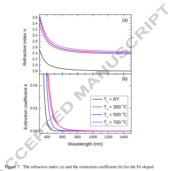
dc reactive magnetron sputtering [14]. The film prepared at room temperature has some cracks as shown in Fig. 3. Although these cracks can result in a decrease of the transmittance by light scattering, it seems that the influence is not very significant as the transmittance is still high. The amplitude of the interference fringes increases significantly when the substrate temperature is increased from room temperature to 300 ºC, which qualitatively indicates an increase in the films’ refractive index, since the oscillation amplitude is related to the difference in the refractive indices of the substrate and the film. The optical constants (thickness, refractive index and extinction coefficient) of the films prepared at different substrate temperatures were obtained by fitting the transmittance using SCOUT software. The fitting result for film prepared at 700 ºC has been given in Fig. 6. The fitting model is composed by a harmonic oscillator which represents a high energy interband transition and the O’Leary-Johnson-Lim (OJL) interband transition which is responsible for the band gap transitions [15]. Although the OJL model has been initially proposed to model the band gap transitions of amorphous silicon, it has been widely used as it gives a good fit to the transmittance with few parameters. The optical thickness of the films is obtained by fitting the transmittance. All the films have a similar thickness, 400 nm. It means the substrate temperature does not affect the deposition rate. The refractive index and the extinction coefficient as a function of the wavelength for the films prepared at different substrate temperatures are shown in Fig. 7. It can be seen that the refractive index has a great increase when the substrate temperature is increased from room temperature to 300 ºC. When the substrate temperature is increased from 300 ºC to 700 ºC, the refractive index shows a small increase. As it can be seen from the XRD patterns, the film prepared at room temperature has an amorphous structure and the films prepared at temperature higher than 300 ºC show the polycrystalline structures. The amorphous structure may have a lower packing density on an atomic level in the glassy state and a high density of defects if the amorphous state is considered a strongly disturbed lattice, which results in a low refractive index. Amorphous structures with low refractive index have analogously been observed for different metallic oxide films [16, 17]. The small increase of the refractive index when the temperature is increased from 300 ºC to 700 ºC may result from the formation of the rutile phase as the rutile phase has a higher refractive index than the anatase phase has. Tanemura has reported the refractive index
for epitaxial rutile TiO2 film which is 2.84 at λ = 500 nm [18]. The refractive index for
our films is lower than the value reported by Tanemura. As it can be seen from the XRD results, the films prepared at temperature higher than 500 ºC have a mixture phase of anatase and rutile, that may result in a low refractive index. The refractive index at λ = 550 nm of the film prepared at 300 ºC is about 2.50 which is very close to the value of the anatase bulk material (n = 2.52 at λ = 550 nm)[19]. It means the film prepared at this temperature has a very high packing density.
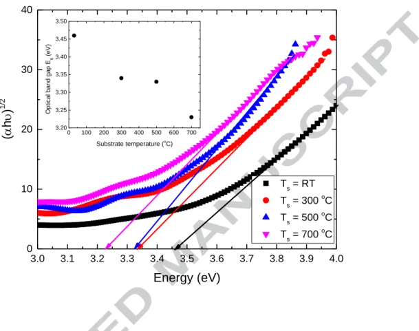
The absorption coefficient α and the optical band gap Eg are related by the following
equation for a semiconductor [20]
(αhν)n = hν – Eg
where ν is the frequency, h is Planck’s constant, and n = ½ for indirect bandgap
transition material [21]. The optical band gap can be estimated from a plot of (αhν)1/2
versus photon energy (hν). The interception of the tangent to the plot will give a good approximation of the optical band gap energy for this indirect band gap material as shown in Fig. 8. The variation of the optical band gap with the substrate temperature is also shown in the figure (inset in Fig. 8). The optical band gap decreases from 3.46 eV to 3.23 eV as the substrate temperature is increased from room temperature to 700 ºC. The film prepared at room temperature has an amorphous structure and a high optical band gap with the value of 3.46 eV, which is similar to the value reported for the amorphous Ti oxide films prepared by sputtering [22]. The film prepared at substrate temperature of 300 ºC shows an anatase structure with an optical band gap of 3.34 eV, which is higher than the value of anatase phase in bulk material (3.20 eV) and lower than the value of the polycrystalline anatase film prepared by sputtering (3.39 eV) [18].
Obviously, the doping of Fe in TiO2 film does not narrow the optical band gap
significantly. The possible reason is that the low Fe concentration in the film is not
enough to modify the optical band gap of TiO2 film. As the temperature is increased
further, the rutile phase appears and the optical band gap decreases because the optical band gap of the rutile phase (3.03 eV) is smaller than that of the anatase phase [18].
Fe-doped TiO2 films have been prepared successfully by pulsed laser deposition at
different temperatures using Fe powder doped TiO2 ceramic target. Although the TiO2
target has a pure rutile phase, the deposited films present an amorphous phase, a pure anatase phase and an anatase-rutile mixing phase when the substrate temperature is room temperature, 300 ºC and higher than 500 ºC. The atomic concentration of Fe atoms in the target is 15 at.%. However, the concentration of Fe in the deposited films is much lower than this value, which means the ablation yield of the Fe atom is much
lower than TiO2. Fe exists in all the films as Fe3+ ionic state although it exists in the
target as Fe atom indicating a fully oxidation in the process of the deposition. The film deposited at room temperature shows a high transmittance, a low refractive index and a large optical band gap. When the substrate temperature increases, the refractive index increases and the optical band gap decreases.
References
[1] Y. Wang, K. Nomura, X. Liu, A.I. Rykov, C. Jin, T. Liu, J. Wang, Structural and Magnetic Properties of Fe-57-Doped TiO2 and Fe-57/Sn-Codoped TiO2 Prepared by a Soft-Chemical Process, Eur J Inorg Chem, (2016) 2131-2135.
[2] S. Larumbe, M. Monge, C. Gomez-Polo, Comparative study of (N, Fe) doped TiO2 photocatalysts, Appl Surf Sci, 327 (2015) 490-497.
[3] S. Kumar, S. Gautam, G.W. Kim, F. Ahmed, M.S. Anwar, K.H. Chae, H.K. Choi, H. Chung, B.H. Koo, Structural, magnetic and electronic structure studies of Mn doped TiO2 thin films, Appl Surf Sci, 257 (2011) 10557-10561.
[4] T. Fukumura, Y. Yamada, H. Toyosaki, T. Hasegawa, H. Koinuma, M. Kawasaki, Exploration of oxide-based diluted magnetic semiconductors toward transparent spintronics, Appl Surf Sci, 223 (2004) 62-67.
[5] N.H. Hong, J. Sakai, W. Prellier, A. Ruyter, Room temperature ferromagnetism in laser ablated transition-metal-doped TiO2 thin films on various types of substrates, J Phys D Appl Phys, 38 (2005) 816-821.
[6] Q.H. Li, L. Wei, Y.R. Xie, F. Jiang, T. Zhou, G.X. Hu, J. Jiao, Y.X. Chen, G.L. Liu, S.S. Yan, L.M. Mei, Effects of oxygen vacancy on the electrical and magnetic properties of anatase Fe0.05Ti0.95O2-delta films, J Alloy Compd, 574 (2013) 67-70.
[7] J.H. Scofield, HARTREE-SLATER SUBSHELL PHOTOIONIZATION CROSS-SECTIONS AT 1254 AND 1487EV, Journal of Electron Spectroscopy and Related Phenomena, 8 (1976) 129-137.
[8] C.E. Myers, H.F. Franzen, J.W. Anderegg, X-Ray Photoelectron-Spectra and Bonding in Transition-Metal Phosphides, Inorg Chem, 24 (1985) 1822-1824.
[9] D.D. Hawn, B.M. Dekoven, Deconvolution as a Correction for Photoelectron Inelastic Energy-Losses in the Core Level Xps Spectra of Iron-Oxides, Surf Interface Anal, 10 (1987) 63-74.
[10] S. Hirose, H. Yoshikawa, H. Yanagi, A. Ando, S. Ueda, N. Ohashi, Impact of Electrode Oxidation on the Current Transport Properties at Platinum/(Niobium-Doped Strontium-Titanate) Schottky Junctions, Ecs J Solid State Sc, 3 (2014) P243-P248.
[11] T. Onoki, Porous Apatite Coating on Various Titanium Metallic Materials via Low Temperature Processing, in: R. Pignatello (Ed.) Biomaterials Science and Engineering, InTech, 2011.
[12] K. Nagaveni, M.S. Hegde, N. Ravishankar, G.N. Subbanna, G. Madras, Synthesis and structure of nanocrystalline TiO2 with lower band gap showing high photocatalytic activity, Langmuir, 20 (2004) 2900-2907.
[13] A. Jilani, J. Iqbal, S. Rafique, M. Abdel-wahab, Y. Jamil, A. Al-Ghamdi, Morphological, optical and X-ray photoelectron chemical state shift investigations of ZnO thin films, Optik - International Journal for Light and Electron Optics, 127 (2016) 8.
[14] L.J. Meng, M.P. Dossantos, Investigations of Titanium-Oxide Films Deposited by Dc Reactive Magnetron Sputtering in Different Sputtering Pressures, Thin Solid Films, 226 (1993) 22-29.
[15] S.K. OLeary, S.R. Johnson, P.K. Lim, The relationship between the distribution of electronic states and the optical absorption spectrum of an amorphous semiconductor: An empirical analysis, J Appl Phys, 82 (1997) 3334-3340.
[16] J.L. Wang, Y.H. Yu, S.C. Lee, Y.W. Chung, Tribological and optical properties of crystalline and amorphous alumina thin films grown by low-temperature reactive magnetron sputter-deposition, Surf Coat Tech, 146 (2001) 189-194.
[17] S. Heiroth, R. Ghisleni, T. Lippert, J. Michler, A. Wokaun, Optical and mechanical properties of amorphous and crystalline yttria-stabilized zirconia thin films prepared by pulsed laser deposition, Acta Mater, 59 (2011) 2330-2340.
[18] S. Tanemura, L. Miao, W. Wunderlich, M. Tanemura, Y. Mori, S. Toh, K. Kaneko, Fabrication and characterization of anatase/rutile-TiO2 thin films by magnetron sputtering: a review, Sci Technol Adv Mat, 6 (2005) 11-17.
[19] G.V. Samsonov, The Oxide Handbook, IFI-Plenum, New York, (1982).
[20] J. Tauc, Absorption Edge and Internal Electric Fields in Amorphous Semiconductors, Mater Res Bull, 5 (1970) 721-&.
[21] G.K. Mor, O.K. Varghese, M. Paulose, C.A. Grimes, Transparent highly ordered TiO2 nanotube arrays via anodization of titanium thin films, Adv Funct Mater, 15 (2005) 1291-1296.
[22] J. Rodriguez, M. Gomez, J. Ederth, G.A. Niklasson, C.G. Granqvist, Thickness dependence of the optical properties of sputter deposited Ti oxide films, Thin Solid Films, 365 (2000) 119-125.
Tables and Figures Captions
Table 1. X-ray diffraction peak parameters for the Fe-doped TiO2 films prepared at different substrate temperatures.
Table 2 XPS parameters for the Fe-doped TiO2 films prepared at different substrate
temperatures.
Figure 1. X-ray diffraction patterns for the target and the Fe-doped TiO2 films prepared
at different substrate temperatures (A: anatase; R: rutile).
Figure 2. Raman spectra for the Fe-doped TiO2 films prepared at different substrate
temperatures (A-TiO2: anatase TiO2; R-TiO2: rutile TiO2).
Figure 3. SEM surface images of the Fe-doped TiO2 films prepared at different
substrate temperatures.
Figure 4. XPS spectra for the Ti 2p (a), O 1s (b) and Fe 2p (c) core levels of the
Fe-doped TiO2 films prepared at different substrate temperatures. (Red dots: experimental
data; Solid black lines: fitting results; Dash blue lines: individual peak fitting results)
Figure 5. Transmittance for the glass substrate and the Fe-doped TiO2 films prepared at
different substrate temperatures.
Figure 6. The transmittance of the film prepared at 700 ºC substrate temperature. (red dot: raw data; black line: fitting result)
Figure 7. The refractive index (a) and the extinction coefficient (b) for the Fe-doped
TiO2 films prepared at different substrate temperatures.
Figure 8. The determination of the band gap energy for the Fe-doped TiO2 films
prepared at different substrate temperatures from the plot of (h)1/2 versus the
excitation energy, h.(Inset is the variation of the optical band gap versus substrate
Table 1. X-ray diffraction peak parameters for the Fe-doped TiO2 films prepared at different substrate temperatures.
Substrate temperature 300 ºC 500 ºC 700 ºC Position 25.23º 25.25º 25.32º A (101) Intensity 1560 567 312 FWHM 0.28º 0.32º 0.38º Crystallite size 30 nm 27 nm 22 nm Position 37.84º 37.76º 37.78º Intensity 1464 4748 7638 A (004) FWHM 0.43º 0.42º 0.23º Crystallite size 20 nm 21 nm 38 nm IA(004)/IA(101) 0.94 8.37 24.48 Position 27.38º 27.40º Intensity 411 1144 R (110) FWHM 0.64º 0.34º Crystallite size 13 nm 25 nm IR(110)/IA(101) 0.72 3.67
Table 2 XPS parameters for the Fe-doped TiO2 films prepared at different
substrate temperatures. Substrate temperature RT 300 ºC 500 ºC 700 ºC Position (eV) 529.96 529.55 529.45 529.46 OI Concentration(at.%) 54.3 50.0 45.0 40.6 FWHM (eV) 1.52 1.46 1.45 1.49 Position (eV) 531.53 531.87 531.92 531.99 O1s OII Concentration(at.%) 18.8 21.8 24.9 36.3 FWHM (eV) 2.07 2.03 2.03 1.77 Position (eV) 533.57 533.47 533.75 OIII Concentration(at.%) 2.4 6.9 4.0 FWHM (eV) 1.12 1.36 1.08 Position (eV) 458.48 458.35 458.21 458.14 Ti2p3/2 Concentration(at.%) 26.4 25.3 22.5 18.3 FWHM (eV) 1.45 1.31 1.30 1.29 OI/Ti 2.1 2.0 2.0 2.2 Position (eV) 710.62 711.15 711.06 710.69 Fe2p3/2 Concentration(at.%) 0.5 0.5 0.7 0.8 FWHM (eV) 3.55 3.38 2.87 2.08
20 25 30 35 40 45 50 55 60 A(112) A(004) R(11 1) R(20 0) Ts = 700 oC Ts = 500 oC Int en sity ( ar b. un its)
Diffraction angle, 2 (deg)
Ts = RT Ts = 300 oC Target A(10 1) R(11 0) R(10 1) Fe (1 10 ) Si (10 0)
Figure 1. X-ray diffraction patterns for the target and the Fe-doped TiO2 films prepared
100 200 300 400 500 600 700 800 Si substrate A-TiO 2 -E g R-TiO 2 -A 1g R-TiO 2 -E g A-TiO 2 -B 1g Ts = 700 oC Ts = 500 oC Int en sity (a rb . u nits) Raman shift (cm-1) Ts = RT Ts = 300 oC A-TiO 2 -E g Si
Figure 2. Raman spectra for the Fe-doped TiO2 films prepared at different substrate
Figure 3. SEM surface images of the Fe-doped TiO2 films prepared at different
Ti 2p1/2 Ts = RT (a) Ti 2p3/2 Ts = 300 oC Ts = 500 oC 456 458 460 462 464 466 468 Ts = 700 oC Inten sity (arb . un its)
Binding energy (eV)
(b) O 1s Ts = RT Ts = 300 oC Ts = 500 oC 528 530 532 534 536 Ts = 700 oC Inten sity (arb . un its)
Binding energy (eV)
Fe 2p1/2 Fe 2p3/2 (c) T s = RT Ts = 300 oC Ts = 500 oC 700 710 720 730 740 Ts = 700 oC Inten sity (arb . un its)
Binding energy (eV)
Figure 4. XPS spectra for the Ti 2p (a), O 1s (b) and Fe 2p (c) core levels of the
Fe-doped TiO2 films prepared at different substrate temperatures. (Red dots: experimental
300 600 900 1200 1500 0 20 40 60 80 100 Tr an smitta nce (%) Wavelength (nm) Bare Substrate Ts = RT Ts = 300 oC Ts = 500 oC Ts = 700 oC
Figure 5. Transmittance for the glass substrate and the Fe-doped TiO2 films prepared at
300 600 900 1200 1500 0 20 40 60 80 100 Fitting line Raw data Tr an smitta nce (%) Wavelength (nm) Figure 6. The transmittance of the film prepared at 700 ºC substrate temperature. (red dot: raw data; black line: fitting result)
1.8 2.0 2.2 2.4 2.6 2.8 3.0 3.2 3.4 3.6 Refr active ind ex n Ts = RT Ts = 300 oC Ts = 500 oC Ts = 700 oC (a) 400 600 800 1000 1200 1400 0.00 0.01 0.02 Extinction coe fficien t k Wavelength (nm) (b)
Figure 7. The refractive index (a) and the extinction coefficient (b) for the Fe-doped
3.0 3.1 3.2 3.3 3.4 3.5 3.6 3.7 3.8 3.9 4.0 0 10 20 30 40 Ts = RT Ts = 300 oC Ts = 500 oC Ts = 700 oC ( h ) 1/2 Energy (eV) 0 100 200 300 400 500 600 700 3.20 3.25 3.30 3.35 3.40 3.45 3.50 O p ti c a l b a n d g a p E g (e V) Substrate temperature (o C)
Figure 8. The determination of the band gap energy for the Fe-doped TiO2 films
prepared at different substrate temperatures from the plot of (h)1/2 versus the
excitation energy, h.(Inset is the variation of the optical band gap versus substrate
Highlights
Fe-doped TiO2 films have been prepared by novel PLD route using its own source.
The chemical state of Fe, Ti and O in the source and film are studied and compared in detail. The optical constants of the film were obtained using the O’Leary-Johnson-Lim model. The deposition temperature determines the structural properties and band gap.