J. Nano- Electron. Phys.
3 (2011) No1, P. 590-600 (Sumy State University) 2011 SumDU
590
PACS numbers: 81.15.Gh, 61.05.c, 68.55.ag, 78.20.ci
NANOSTRUCTURED HYDROGENATED SILICON FILMS BY HOT-WIRE CHEMICAL VAPOR DEPOSITION: THE INFLUENCE OF SUBSTRATE
TEMPERATURE ON MATERIAL PROPERTIES
V.S. Waman1, M.M. Kamble1, M.R. Pramod1, A.M. Funde1, V.G. Sathe2, S.W. Gosavi3, S.R. Jadkar3*
1 School of Energy Studies, University of Pune, Pune, 411 007, India
2 UGC-DAE-CSR, University Campus, Khandawa Road, Indore, 452 017, India 3 Department of Physics, University of Pune, Pune, 411 007, India
E-mail: *sandesh@physics.unipune.ac.in
Thin films of hydrogenated nanocrystalline silicon are prepared at reasonably higher deposition rates (9-13 /s) by indigenously fabricated hot-wire chemical vapor deposition system at various substrate temperatures (Ts). In this paper we report extensively studied structural, optical and electrical properties of these films by Fourier transform infrared (FTIR) spectroscopy, low angle X-ray diffraction (low angle XRD), micro-Raman spectroscopy and UV-Visible spectroscopy. The low angle XRD and micro-Raman spectroscopy analysis indicate amorphous-to-nanocrystalline transition occurred at Ts 300 C. It is observed that volume fraction of crystallites and its size increases with increase in Ts. The low angle XRD study also shows nc-Si:H films with well-identified lattice planes of (111) orientation. In addition, it is observed from the FTIR spectroscopy that the hydrogen is incorporated in the film mainly in Si-H2 and (Si-H2)n complexes. The nc-Si:H films with low hydrogen content (< 4 at. %) and wide band gap (1.83-1.89 eV) and low refractive index (< 3) is useful for various device applications.
Keywords: HOT WIRE CHEMICAL VAPOR DEPOSITION, NANOCRYSTALLINE SILICON THIN FILMS, STRUCTURAL PROPERTIES, OPTICAL PROPERTIES, ELECTRICAL PROPERTIES.
(Received 04 February 2011, in final form 18 June 2011)
1. INTRODUCTION
NANOSTRUCTURED HYDROGENATED SILICON FILMS BY… 591
In general there are two methods used for the synthesis of nc-Si:H thin films, one is the re-crystallization of a-Si:H films and other is the direct deposition. The re-crystallization technique includes rapid thermal annealing [5], laser melt re-crystallization [6], aluminium induced crystallization [7] etc. However, these methods have difficulties in accurate control of crystallite size and crystalline volume fraction. In addition, post annealing at temperatures over 1000 C is generally required for the crystallization of Si nanoparticles. Such high annealing temperature inevitably limits its further applications in opto-electronic devices. On the other hand, a variety of direct chemical vapor deposition (CVD) techniques has been used to yield materials with good opto-electronic properties. These include plasma enhanced-CVD (PE - CVD) [8] and its variant, very high frequency glow discharge [9]. Other CVD methods employed in the deposition of nc-Si:H are electron cyclotron resonance CVD [10], homo CVD [11], low energy PE CVD [12] and hot wire CVD (HW CVD) [13]. Among these, only PE CVD has been established for industrial applications [14]. The high RF power and high hydrogen dilution of silane are the two critical parameters in conventional PE - CVD method that facilitate nanocrystallization [15]. The high RF - power causes surface damage by high-energy ion bombardment and high hydrogen dilution of silane retards the deposition rate of nc-Si:H films [16] and have constrained the film deposition to a narrow substrate temperature range [17]. The lower deposition rate increases the process operation time and hence the cost whereas narrow substrate temperature range involves difficulty in controlling the hydrogen distribution in the film, which is responsible for light-induced degradation of electronic properties [18].
Hot wire chemical vapor deposition (HW - CVD) or simply ‘hot-wire method’ has received considerable attention in recent years as an alternative deposition method for the synthesis of nc-Si:H [19] films because it is capable of improving film stability and of achieving higher deposition rates. This technique appears to be capable of providing easy control of the production of unknown higher order silane whose gas phase reactions generally lead to the incorporation of undesirable excess hydrogen in the film. Moreover, the technique involves very few deposition parameters which can easily be optimized, and the film growth processes involve simple radicals which are primarily atoms (atomic Si and atomic H) released from the hot surface [20]. Despite these economically important features and technological simplicity, this technique has received much less attention for the synthesis of nc-Si:H thin films.
592 V.S. WAMAN, M.M. KAMBLE, M.R. PRAMOD, ET AL.
2. EXPERIMENTAL 2.1 Film preparation
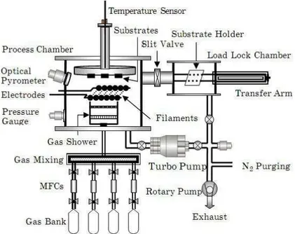
Figure 1 shows the schematic of dual chamber HW - CVD system recently established at School of Energy Studies, University of Pune. The apparatus consists of two stainless steel chambers, referred as process chamber and load lock chamber. The process chamber is coupled with a turbo molecular pump which yields a base pressure less than 10 – 6 Torr. The use of load lock chamber prevents the process chamber to be directly exposed to air, which minimizes the pump down time and reduce contamination of layers with oxygen and water vapours. The substrates can be moved from load lock to process chamber by a pneumatically controlled transport arm. The pressure during deposition was kept constant by using automated throttle valve. For deposition we have used 10 straight tungsten filaments that are mounted parallel to each other, separated 1 cm apart. Each filament has a diameter of 0.5 mm and a length of 10 cm. Heating of filaments is done by sending an AC current through the wires by using a current transformer and dimmer. The filament temperature is determined by optical pyrometer (IRCON Infrared thermometer, USA). A shutter is placed in front of the substrates to shield the substrates from undesired deposition during pre-heating of filaments. The reaction gas was introduced in the process chamber from the bottom and perpendicular to the plane of the filaments through a specially designed gas shower to ensure uniform gas flow over the filaments. The substrates can be placed on substrate holder which is heated by in build heater and substrate temperature varied by using thermocouple and temperature controller. Other process parameters are listed in Table 1. Films were prepared by using pure SiH4 gas (MSG).
NANOSTRUCTURED HYDROGENATED SILICON FILMS BY… 593
Table 1 – Deposition parameters employed for the synthesis of Si:H films by HW-CVD
1. Filament temperature (Tfil) 1900 C 2. Deposition pressure (Pdep) 40 mTorr 3. Substrate temperature (Tsub) 100-450 5 C
4. SiH4 flow rate 5 sccm
5. Filament to substrate distance (ds-f) 6 cm
6. Deposition time (t) 10 Minutes
2.2 Film characterization
Dark conductivity (dark) and photoconductivity (photo) were measured with coplanar Al electrodes at room temperature and atmospheric pressure. Fourier transform infrared (FTIR) spectra of the films were recorded by using FTIR spectrophotometer (Shimadzu, Japan). Bonded hydrogen content (CH) was calculated from wagging mode of IR absorption peak using the method given by Brodsky et al. [22]. The microstructure parameter (R*) is determined by using I2100/(I2000 + I2100), where I2000 and I2100 are the integrated absorption intensities at 2000 cm – 1 and 2100 cm – 1 respectively. The refractive index and energy band gap were deduced from Swanepoel method [23]. Raman spectra were recorded with micro-Raman spectroscopy (Jobin Yvon Horibra LABRAM-HR) in the wavelength range 400-700 nm. The Raman spectra were deconvoluted in the range 400-540 cm – 1 using Levenberg-Marquardt method [24]. The crystalline fraction (XRaman) and crystallite size (dRaman) was then deduced using the method proposed by Kaneko et al. [25] and He et al. [26]. Low angle X-ray diffraction patterns were obtained by X-ray diffractometer (Bruker D8 Advance, Germany) using CuK line ( 1.54056 ). The patterns were taken at a grazing angle of 1. Average crystallite size was estimated using the Scherrer's formula [27]. Thickness of films was determined by Talystep profilometer (Taylor-Hobson) and confirmed by UV-Visible spectroscopy using the method proposed bySwanepoel[23].
3. RESULTS AND DISCUSSION 3.1 Variation in deposition rate
594 V.S. WAMAN, M.M. KAMBLE, M.R. PRAMOD, ET AL.
Fig. 2 – Variation of the deposition rate as a function of substrate temperature
3.2 Micro-Raman spectroscopic analysis
Raman spectroscopy is a very powerful non-destructive technique that gives a fast and simple way to determine the phase of the material, whether it is amorphous, crystalline or nanocrystalline. Figure 3 shows the Raman spectra of the silicon films deposited at different Ts ranging from 100 C to 450 C. Each spectrum shown in figure was de-convoluted into three peaks with a suitable base line. The inset show a typical de-convoluted Raman spectra into amorphous and crystalline components for the film deposited at Ts 400 C. The estimated values of crystallite size (dRaman) and volume fraction of crystallites (XRaman) are also shown in the Figure 3.
Fig. 3 – Raman spectra of nc-Si:H films for different substrate temperature. The inset show the de-convolution of Raman spectra for the film deposited at Ts 400 C
NANOSTRUCTURED HYDROGENATED SILICON FILMS BY… 595
1) The films deposited at low substrate temperatures (Ts 300 C) show only a broad shoulder at 480 cm – 1, indicating that the film is in a purely amorphous phase.
2) Raman spectrum for the film deposited at Ts 300 C shows a broad peak centered at 479 cm-1 and a sharp peak at 517 cm – 1 are attributed to the transverse optical (TO) mode of Si–Si vibrations in the amorphous and crystalline phases, respectively [30-32]. For this film volume fraction of crystallite (XRaman) is 42 % and crystallite size (dRaman) is 4.6 nm. Thus, Raman scattering study clearly indicates that the nc-Si:H films synthesized by HW - CVD are a mixture of two phases, an amorphous phase and a crystalline phase with nano-size Si crystals embedded in amorphous matrix.
3) With further increase in Ts, the intensity and sharpness of peak 517 cm-1 increases indicating increase in X
Raman and dRaman. The increase in volume fraction of crystallite and crystallite size can be attributed to the enhancement in the nucleation rate with increasing substrate temperature.
These results are consistent with low angle X-ray diffraction results (discussed later) and provide strong support to the formation of nc-Si:H films.
3.3 Low angle X-ray diffraction analysis
596 V.S. WAMAN, M.M. KAMBLE, M.R. PRAMOD, ET AL.
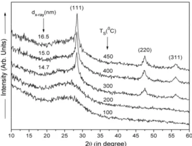
Fig.4 X-ray diffraction pattern of nc-Si:H films deposited at different substrate temperature
3.4 FTIR spectroscopic analysis
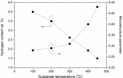
Figure 5 shows the variation of hydrogen content (CH) and microstructure parameter (R*) as a function of substrate temperature (Ts) for nc-Si:H films deposited by HW - CVD. As seen from the figure, CH in the film decreases from 4 at. % to 1.5 at. % when Ts increases from 100 to 450 C. The decrease in hydrogen content with increase in the substrate temperature has been reported by many authors [33, 35] and is attributed to the increase in mobility of H on the hot surface with increase in the substrate temperature. The low hydrogen content in the nc-Si:H films deposited at high substrate temperature can also be correlated with the increased crystallinity in the films [36]. Raman spectroscopic and low angle x-ray diffraction analysis further supports this. Moreover, during the growth, the films undergo in-situ annealing due to the radiation coming from the filaments, which causes the evolution of hydrogen. With increase in substrate temperature, the evolution of hydrogen becomes stronger and hydrogen content in the film decreases [37].
Furthermore, it can be seen from the figure that the microstructure parameter (R*) increases from 0.28 to 0.48 with increase in substrate temperature indicating that the hydrogen-bonding configuration in the films changes from Si-H group to SiH2 group with increase in substrate temperature.
3.5 UV-Visible spectroscopy analysis
NANOSTRUCTURED HYDROGENATED SILICON FILMS BY… 597
Fig. 5 – Variation of hydrogen content and microstructure parameter of Si:H films as a function of substrate temperature
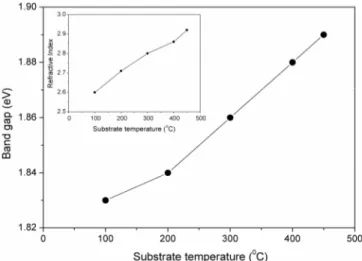
the figure, the band gap of nc-Si:H films increases from 1.83 eV to 1.89 eV as substrate temperature increases from from 100 to 450 C. It is well established that the band gap of hydrogenated amorphous silicon (a-Si:H) deposited by HW - CVD and PE - CVD methods increases with increase in hydrogen content in the film [38, 39]. However, in the present study we have observed decrease in hydrogen content with increase in substrate temperature (see Figure 5). Thus, only the number of Si-H bonds cannot account for increase band gap in nc-Si:H films in HW-CVD deposited films. We believe that the increase in band gap in HW - CVD grown nc-Si:H films may be due to the increase in crystallinity in the film with increase in substrate temperature as revealed from Raman spectroscopic and x-ray diffraction analysis. This inference is further strengthened by the observed variation in static refractive index (no) of the films with substrate temperature (inset of Figure 6). It is interesting to note that the values of
no has been found less than the value of static refractive index of c-Si (no,c-Si 3.42) over the entire range of substrate temperature studied. These results suggest that the stress in the nc-Si:H films gets relaxed with increasing the substrate temperatures.
3.6 Variation in electrical properties
Figure 7 shows the variation of room temperature dark conductivity (dark) and photoconductivity (photo) as a function of substrate temperature. A gradual and systematic change in the electrical properties of the material happens to take place when the deposition temperature is increased from 100 to 450 C. At Ts 100 C the film exhibited dark ~ 3 10 – 10 S/cm and
photo ~ 2 10 – 6 along with a photosensitivity gain (defined as
photo/dark) of ~ 104. The high photosensitivity gain signifies its amorphous dominated structure. As a temperature increases the dark is noticeably increased by five orders of magnitude to ~ 10 – 6 S/cm, whereas
598 V.S. WAMAN, M.M. KAMBLE, M.R. PRAMOD, ET AL.
Fig. 6 – Variation in the optical band gap and static refractive index of the nc-Si:H films with substrate temperature
Fig. 7 – Room temperature dark conductivity and photoconductivity of the films prepared at different substrate temperatures
NANOSTRUCTURED HYDROGENATED SILICON FILMS BY… 599
4. CONCLUSIONS
Effects of substrate temperature on structural, optical and electrical properties of nc-Si:H films deposited by HW - CVD have been studied in detail. The formation of nc-Si:H films have been confirmed by micro-Raman spectroscopy and Low angle x-ray diffraction analysis. We have observed amorphous-to-nanocrystalline phase transition at substrate temperature 300 C. Further increase in substrate temperature the crystallinity and the crystallite size in the films improves. The FTIR spectroscopic studies showed that the hydrogen content in the film decreases with increase in substrate temperature and is found < 4 at. % over the entire range of substrate temperature studied. In addition, it is also observed that the hydrogen incorporated in the film mainly in Si-H2 and (Si-H2)n complexes. However, the band gap showed increasing trend with increase in substrate temperature. We attribute increase in band gap due to increase in crystallinity in the film.
The authors SRJ, VSW, AMF and MMK are thankful Department of Science and Technology (DST) and Ministry of New and Renewable Energy (MNRE), Government of India and Centre for Nanomaterials and Quantum Systems (CNQS), University of Pune for the financial support.
REFERENCES
1. P.V. Shah, J. Meier, E. Vallat-Sauvain, N. Wyrsch, U. Kroll, C. Droz, U. Graf,
Sol. Energ. Mater. Sol. C. 78, 469 (2003).
2. J. Kitao, H. Harada, N. Yoshida, Y. Kasuya, M. Nishio, T. Sakamoto, T. Itoh, S. Nonomura, Sol. Energ. Mater. Sol. C. 66, 245 (2001).
3. R. Saleh, and N. Nickel, Thin Solid Films 427, 266 (2003).
4. R. Schropp, H. Li, R. Franken, J. Rath, J. Schuttauf, R. Stolk, Thin Solid Films 516, 6818 (2008).
5. H.C. Cheng, C.Y. Huang, F.S. Wang, K.H. Lin, F.G. Tarntair, Jpn. J. Appl. Phys. 39, L19 (2000).
6. T.E. Dyer, J.M. Marshall, W. Pickin, A.R. Hepburn, J.F. Davies, J. Non-Cryst. Solids 164-166, 1001 (1993).
7. A.G. Aberle, N.P. Harden, S. Oelting, J. Cryst. Growth 226, 209 (2001). 8. Y. Nasuno, M. Kondo and A. Matsuda, Jpn. J. Appl. Phys. 41, 5912 (2002). 9. A. Shah, J. Meier, E. Vallat-Sauvain, C. Droz, U. Kroll, N. Wyrsch, J. Guillet,
U. Graf, Thin Solid Films 403-404, 179 (2002).
10. H.L. Hsiao, H.L. Hwang, A.B. Yang, L.W. Chen, T.R. Yew, Appl. Surf. Sci. 142, 316 (1999).
11. B.A. Scott, J.A. Reimer, R.M. Plecenik, E. Esimonyi, W. Reuter, Appl. Phys. Lett.
40,973 (1982).
12. M. Acciarri, S. Binetti, M. Bollani, A. Comotti, L. Fumagalli, S. Pizzini, H. Von Kanel, Sol. Energ. Mat. Sol. C. 87, 11 (2005).
13. M. Fonrodona, D. Soler, J. Escarre, F. Villar, J. Bertomeu, J. Andreu, A. Sabou-ndji, N. Coulon, T. Mohammed-Brahim, Thin Solid Films 501, 303 (2006). 14. R. Saleh, N.H. Nickel, Thin Solid Films 427, 266 (2003).
15. D. Das, J. Phys. D: Appl. Phys. 36,2335 (2003).
16. A.B. Pevtsov, N.A. Feoktistov, Tech. Phys. Lett. 28/4, 305 (2002).
17. T. Shimizu, K. Nakazawa, M. Kumeda, S. Ueda, Physica B/C 117/118, 926 (1983). 18. P. Santos, N. Johnson, R. Street, Phys. Rev. Lett. 67, 2686 (1991).
19. M. Scriba, D. Britton, C. Arendse, M. Harting, Thin Solid Films 517/12, 3484
600 V.S. WAMAN, M.M. KAMBLE, M.R. PRAMOD, ET AL.
20. C. Horbach, W. Beyer, H. Wagner, J. Non-Cryst. Solids 137, 661 (1991). 21. P. Gogoi, H.S. Jha, D. Deva, P. Agarwal, phys. status solidi C 7, 592 (2010). 22. M. Brodsky, M. Cardona, J. Cuomo, Phys. Rev. B 16, 3556 (1977).
23. R. Swanepoel, J. Phys. E: Sci. Instrum. 16, 1214 (1983). 24. D. Marquardt, J. Soc. Ind. Appl. Math. 11/2, 431 (1963).
25. T. Kaneko, M. Wakagi, K. Onisawa, T. Minemura, Appl. Phys. Lett. 64, 1865 (1994). 26. Y. He, C. Yin, G. Cheng, L. Wang, X. Liu, G.Y. Hu, J. Appl. Phys. 75, 797 (1994). 27. H. Klung, L. Alexander, X-ray Diffraction Procedures (New York, Wiley: 1974). 28. S. Klein, F. Finger, R. Carius, J. Lossen, M. Stutzmann, J. Appl. Phys. 98, 024905
(2005).
29. S. Kumar, P. Dixit, C. Rauthan, J. Gope, J. Phys: Condens. Matter 20, 335215
(2008).
30. Y. Song, E.C. Cho,G. Conibeer, C. Flynn, Y.D. Huang, M.A. Green, Sol. Energ. Mater. Sol. C. 92, 474 (2008).
31. Z.M. Wu, Q.S. Lei, X.H. Geng, Y. Zhao, J. Sun, J.P. Xi, Chin. Phys. Soc. 15, 1320 (2006).
32. S. Mukhopadhyay, C. Das, S. Ray, J. Phys. D: Appl. Phys. 37, 1736 (2004). 33. C. Das, S. Ray, Thin Solid Films 403-404, 81 (2002).
34. Y. Sun, T. Miyasato, J.K. Wigmore, J. Appl. Phys. 85,3377 (1999).
35. M. Zhu, Y. Cao, X. Guo, J. Liu, M. He, K. Sun,Sol. Energy Mat. Sol. C. 62/1,
109 (2000).
36. S. Wagner, S.H. Wolff, J.M. Gibson, Mater. Res. Soc. Symp. Proc. 164, 161 (1990). 37. Y. Park, S. Rhee, J. Appl. Phys. 90, 217 (2001).
38. A. Singh, E. Devis, J. Non-Crys. Solids 122, 223 (1990).