Design of Bode-type Amplitude Equalizers
with the Specified Shaping Function and
Whole Range
Tejmal S. Rathore1 and Uday P. Khot2
1
Electronics and Telecommunication Engineering Department, St. Francis Institute of Technology, Borivali (W), Mumbai 400 103, India.
tsrathor@ee.iitb.ac.in
2
Electronics and Telecommunication Engineering Department, Thadomal Shahani Engineering College, Bandra (W), Mumbai 400 050, India.
upk@ee.iitb.ac.in
Abstract—A simple design for realizing a Bode-type amplitude equalizer is proposed. It allows any arbitrary, but
RC realizable, shaping function and whole range. The Bode-type amplitude equalizer using current feedback amplifier is derived which can operate satisfactory at much higher frequencies compared to the operational amplifier based ones. Simulation results are in good agreement with the theoretical ones.
Keywards—Bode-type amplitude equalizer, Current feedback amplifier, Whole range, Voltage-mode, Current-mode, Grounded resistor.
I. INTRODUCTION
The transfer function
H X
XH s
T
+ + =1
)
( (1)
suitable for a single resistance variable amplitude equalizer (SRVAE) has been suggested by Bode [1]. It has the interesting characteristics: (1) When X = 0, T(s) = 1/H and when X = ∞, T(s) = H. The H is called the shaping function. T(s) exhibits flat response when X = 1. Thus, a geometric variation of X from 0 to ∞ around 1 results in an arithmetic variation of the logarithmic frequency response. (2) The X is a dimension less number. It is usually a function of a variable resistance RV. The difference in the corresponding values of RV required to realize T(s) as H and 1/H is called the whole range (WR). The WR for T(s) given by (1) is [0, ∞]. (3) When X → 1/X, T(s) → 1/T(s) = G(s). Thus one has to realize only T(s) or G(s). Inverse is obtained by replacing X by 1/X. (4) When H→ 1/H, T(s) →G(s). (5) The X and H are interchangeable.
Several SRVAEs [2]-[6], are known. Saraga and Zyoute [2] realize T(s) as given in (1) with H = Z/(Z + Ro) where Ro is a reference resistance. Thus the WR is [∞, 0]. Their circuit requires 2 op-amps (OAs), one for negative impedance converter (NIC) and another for buffer. Though Brglez’s SRVAE [3] is cascadable and has the same H but WR [0, 2Ro], it also needs an NIC. Zyoute [5] proposed a single OA cascadable equalizer with H = Z/(Z + 2Ro) and WR is [0, ∞]. Since a practical variable resistance cannot have an infinite range, Talkhan et al. [6] has reduced the WR to [0, Ro] for the same circuit by choosing different values for the circuit elements. In the above SRVAEs, block H does not appear explicitly in the circuit. Hence, one has to accept whatever H is realized. Nowrouzian and Fuller [7] proposed a block diagram for realizing G(s) for any specified H, but with a WR [0, ∞]. They have given an example for realizing G(s) with
Z R
Z R H
o o
− +
= . It requires (after correction) 5 OAs. Nowrouzian et al. [8] has also given another method in which specified H is converted into shaping function Z
and then G is realized by inserting Z in a 3-port resistive network. It also has the WR [0, ∞].
In this paper, we suggest a design that can accommodate any specified (but realizable) H and also any desired WR.
II. DESIGN
Transfer function given by (1) can be expressed as XH H XH X s G
+ + + =
1 1 )
( . (2)
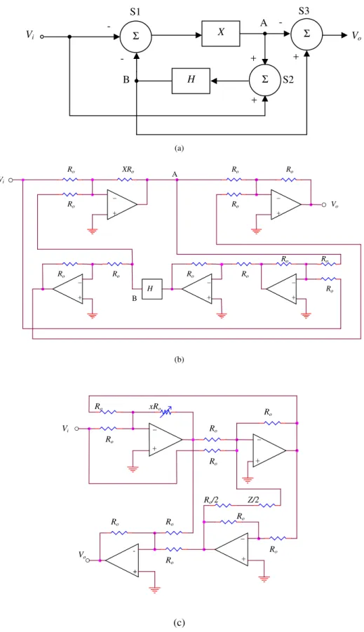
One can easily conceive a block diagram for G as shown in Fig. 1(a). However, it requires two X and two H
input Vito block H, an additional signals –XH/(1 + XH) and XH/(1 + XH) appear at nodes A and B, respectively. Being equal and opposite, they cancel in the summer S3. Now it realizes G with whatever H is inserted in the H
block. The actual circuit obtained from the block diagram of Fig. 1(b) is shown in Fig. 2(a). Some of the inverters can be dispensed with and the final reduced circuit is shown in Fig. 2(b). Note that all the OAs have non-inverting terminal grounded. An alternative circuit is obtained by interchanging the X and H blocks and shown in Fig. 3. The circuit requires 4 OAs, 10 resistors, one variable resistor and a H block. One OA can be reduced if we replace the inverter and the summing amplifier shown in the dashed box of Fig. 2(b) by a difference amplifier as shown in Fig. 4.
(a) (b)
Fig. 1. (a) Block diagram for realizing G and (b) Modified block diagrams for realizing G with specified H
Ro
-1
Vo Ro
-1 Ro
-o
Ro
- A
Ro
-+
+
B R
o
+
H
Ro
-1
o
Ro
Ro X
Vi
(a)
+
Ro
+
-0 o
Ro
-Vi
-Ro
Ro
Ro
Ro
o
Ro
Ro
Ro
Vo
B
A X
H
+
Ro
Ro
+
-Ro
Vi
Ro
Ro
Ro
Ro
+ Ro
o
+
-H
o
Ro
X
Ro
Ro
-Ro
+
Vo
Ro
-Fig. 3. Circuit for realizing G
Fig. 4. Difference amplifier
Example: Consider
Z R
Z R H
o o
− +
= . (3)
Its realizations are shown in Fig. 5. The complete realization of G is shown in Fig. 6 with H shown in Fig. 5(a) and after simplification in Fig. 7. One OA can be reduced if we use an alternate realization of H as shown in Fig. 5(b).
There may be other possible block diagrams for realizing G. One of them is shown in Fig. 8(a). The corresponding circuit and its simplified version are given in Figs. 8(b) and 8(c), respectively. Note that, here we require only 4 single-ended OAs while Nowrouzian and Fuller [7] require 5 OAs (after correction, i.e., including one additional inverter around OA4 and taking shaping function as Z/2 in place of Z as shown in Fig. 7).
(a) (b)
Fig. 5. Realizations of H given by (3)
-VA - Vi o
Vi
o Ro
o
Ro
+
Ro
VA
Ro
Ro
Z/2
Vb
Ro
o
o
+
-Va
-Ro
Ro
+ Ro/2
Ro
o
-Va
o
Ro
Z
Vb
+
Ro
-o
+
- Ro
Ro
o
-Ro
Ro
+
Ro
Ro
+
Ro
A
-Ro
Ro
Ro
Ro
+
Vi
+ +
Vo
B
-Ro
X
Ro Ro
Z/2 Ro/2
Fig. 6. Realization of G for H given by (3)
+
OA3
Ro/2
o
Ro
Vi
OA5
-Ro
Ro
-OA2
Ro
Ro
-o Ro
Ro Ro
Ro
OA1
+
x
+
Vo
Ro
+
Z/2
Ro
OA4
Ro
Ro
-+
Fig. 7. Simplified circuit for realizing G
III.REALIZATION WITH SPECIFIED WR
Circuit realizing the X block can be replaced by the block shown in Fig. 9. This makes the new gain as X
N −
1 where N is real and positive. Thus the WR becomes [N, 0] and can be adjusted as per desire by choosing
the value of N. It is interesting to note that the variable resistance is now grounded. IV.CFABASED REALIZATION
Using voltage-mode (VM) to current-mode (CM) transformation [9], one can convert the OA based VM SRVAE given in Fig. 8(c) into current feedback amplifier (CFA) based CM SRVAE as shown in Fig. 10. As the bandwidth of CFA is much higher than that of OA, the CFA based amplitude equalizer can work well at high frequency compared to OA based ones.
V. SIMULATION RESULTS
(a)
+
Ro
Vo
-+
+
XRo
+
o
H B
A Ro
Vi
Ro
o
-Ro
Ro
Ro
Ro
Ro
+
-Ro Ro
-Ro
Ro
(b)
Ro
xRo
Vi
Ro
Ro
Ro
Ro
Ro
Ro
Ro
Z/2
+
Ro/2
o
-Vo
-Ro
Ro
o
-+
+
-+
(c)
Fig. 8. (a) Alternative block diagram for realizing G, (b) circuit realization, and (c) reduced circuit
Σ X Σ
Vi Vo
S1 S3
-
-
-
+ A
Σ
H S2
+
-Ro
Vi
+ Ro
Ro o
-Ro
-+
Vo B
(X/N)
o +
o
Ro
Ro
Ro A
Fig. 9. Replacement of block X
Ro
y
CFA
Ro/2
Ro
o Ro
CFA x
w
y z
Ro
z
Ro
Z/2 Io
x w
y Ro
x w
CFA
z
>
z
Ro Ro
w Ii
Ro
v
x y
CFA
xRo
Ro
Fig. 10. CFA based realization of G
Fig. 11. Frequency response of the SRVAE circuit given in Fig. 6
VI.CONCLUSIONS
Design of Bode-type amplitude equalizers with a specified but RC realizable shaping function and desired value of whole range has been given. The design leads to an equalizer with grounded variable resistance, which is economical in integrated circuit fabrication. The CFA counterpart for realizing high frequency Bode-type current transfer functions has been given. As the bandwidth of CFA is much higher than that of OA, the CFA based amplitude equalizer can work well at high frequency compared to OA based ones. The simulation results are in good agreement with the theory.
REFERENCES [1] H. W. Bode, “Variable equalizers,” Bell Syst. Tech. J., vol. 17, pp. 229-244, 1938.
[5] M. Zyoute, “New active RC Bode-type variable equaliser,” IEE Proc. G Electronic Circuits and Systems, vol. 128, 1981, pp. 134-137.
[6] E. A. Talkhan, A. M. Soliman, and T. H. El-Fayoumi, “New family of active RC variable equalisers,” Electron. Letter, vol. 20, no. 12, pp. 497-498, 1984.
[7] B. Nowrouzian and A. T. G. Fuller, “A novel approach to the design and synthesis of higher-order Bode-type variable-amplitude active-RC equalizers,” in Proc. IEEE ISCAS'03, May 2003, vol. 1, pp. 513-516.
[8] B. Nowrouzian, A. T. G. Fuller, and M. N. S. Swamy, “Design of arbitrary-order minimal operational amplifier BIBO stable Bode-type variable-amplitude active-RC equalizers,” in Proc. IEEE ISCAS'04, 2004, pp. I-1032-I-1035.
[9] T. S. Rathore and U. P. Khot, “Voltage-mode to current-mode transformation,” in Proc. SPIT-IEEE Colloquium 2007 and Int. Conf., Feb. 2008, Mumbai, India, paper no. C-109.
[10] Orcad EDA software, Cadence Design Systems, Inc., USA.
AUTHORS PROFILE
T S Rathore was born in Jhabhua (M P, India) on Oct. 29, 1943. He received the B Sc (Electrical Engineering), M E (Applied Electronics & Servomechanisms), and Ph D (by research on Passive and Active Circuits) degrees in Electrical Engineering from Indore University, Indore, India in 1965, 1970 and 1975, respectively.
He served SGSITS, Indore from 1965 to 1978 before joining the EE Department of IIT Bombay from where he retired as a Professor on superannuation in June 2006. Currently, from July 2006, he is the Dean (R&D) and Head of Electronics & Telecommunication Department at St. Francis Institute of Technology, Borivali.
He was a post-doctoral fellow (1983-85) at the Concordia University, Montreal, Canada and a visiting researcher at the University of South Australia, Adelaide (March-June 1993). He was an ISTE visiting professor (2005-2007). He has published and presented over 200 research papers in various national/international journals and conferences. He has authored the book Digital Measurement Techniques, New Delhi: Narosa Publishing House, 1996 and Alpha Science International Pvt. Ltd., U K, 2003 and translated in Russian language in 2004. He was the Guest Editor of the special issue of Journal of IE on Instrumentation Electronics (1992). He is a member on the editorial boards of ISTE National Journal of Technical Education and IETE Journal of Education. He has witnessed, organized and chaired many national/international conferences and in some he was also the Chief Editor of the proceedings.
His areas of teaching and research interest are Analysis and Synthesis of Networks, Electronic Circuit Design, Switched-Capacitor Filters, Electronic-Aided Instrumentation, Hartley Transform, Signal Processing, Fault Diagnosis and Knowledge-Based Systems.
Prof. Rathore is a Senior Member of IEEE (USA), Fellow of IETE (India), Fellow of IE (India), Member of ISTE (India), Member of Instrument Society of India, Member of Computer Society of India. He has been listed in Asia’s Who’s Who of Men and Women of achievement (1991). He has played a very active role as Fellow of IETE and has served its Mumbai Centre as Volunteer member (1997-98), Co-opted member (1998-99), Secretary (1999-2001), Chairman (2001-02), Vice Chairman (2003-06) and Chairman (2006-08).
He has received IETE M N Saha Memorial Award (1995), IEEE Silver Jubilee Medal (2001), ISTE U P Government National Award (2002), ISTE Maharashtra State National Award (2003), IETE Prof S V C Aiya Memorial Award (2004), IETE BR Batra Memorial Award (2005), IETE Prof K Sreenivasan Memorial Award (2005). IETE K S Krishnan Memorial Award (2009), IETE - Hari Ramji Toshniwal Gold Medal Award (2010), and IETE best paper award published in IETE J of Education (2011).
Uday P Khot was born in Kolhapur (MS) on June 15, 1970. He obtained B. E. (Ind. Electronics) from Amaravati University in 1991 and M. Tech. (Control and Instrumentation) from IIT Bombay in 1999 and Ph D (by research on Synthesis of Analog Circuits Employing Current-Mode Building Blocks) in Electrical Engineering from IIT Bombay, India in January 2010.
He served Bharati Vidyapeet's Institute of Technology, Navi Mumbai from 1992 – 1999 as a lecturer and Thadomal Shahani Engineering College, Mumbai, as an Assistant Professor from 1999 – 2006. He is an Associate Professor since January 2006. From January 2010, he is the Head of Electronics & Telecommunication Department at Thadomal Shahani Engineering College, Mumbai.
Dr Khot is a Fellow Member of IETE (India), Member of ISTE (India), Member of IEEE (USA) and Member of IE (India). He has been listed in the International Who’s Who of Professionals Historical Society having demonstrated exemplary achievement and distinguished contributions to the business community, edition 2010-2011. He has served IETE Mumbai Centre as a Member (2004-2008).