Design and Implementation of Schmitt Trigger using Operational
Amplifier
Md. Moyeed Abrar
Assistant Professor, Department of Computer Science Engineering, Khaja Banda Nawaz College of Engineering, Kalaburagi, Visvesvaraya Technological university, Belagavi, Karnataka, India.
ABSTRACT
A Schmitt trigger is an electronic circuit, a Comparator that is used to detect whether a voltage has crossed over a given reference leve l. It has two stable states and is very useful as signal conditioning device. Whe n an input waveform in the form of sinusoidal waveform, triangular waveform, or any other periodic waveform is given, the Schmitt trigger will produce a Rectangular or square output waveform that has sharp leading and trailing edges. Such fast rise and fall times are desirable for all dig ital circuits. The state of the art presented in the paper is the design and imple mentation of Sch mitt trig ger using operational a mplifie r µA-741, generating a Rectangular waveform. Fu rthermore, the Schmitt trigger e xh ibiting hysteresis is also presented in the paper. Due to the phenomenon of hysteresis, the output transition from HIGH to LOW and LOW to HIGH will take place at various thresholds.
Keywords
:
Comparator, dig ital c ircu its, hysteresis, operational amplifie r µA-741, rectangular waveform, Schmitt trigger,I.
INTRODUCTION
Noise is any type of unwanted signal or disturbance that is not derived from or harmonica lly related to the input signal. Electric motors, neon signs, power lines, car ignitions, lightning and so on , produce electromagnetic fie lds that can induce noise voltages into electronic circuits. Power supply ripple is also classified as noise since it is not related to the input signal. By the use of regulated power supplies and shielding, the ripple and induced noise can be minimized to an acceptable level. If the input to a comparator contains noise in large a mounts, then obviously the output will be e rratic when input voltage is near the trip point. One possible way to minimize the effect of noise is to use a comparator with positive feedback. Two separate trip points would be produced with positive feedback that helps to prevent a noisy input fro m producing fa lse transitions. Thus the standard solution for a noisy input is to use a comparator with positive feedback which is usually called a Sch mitt trigger [1], [2].
The Sch mitt trigger is also called as a Squaring circuit, as it converts an irregular shaped input waveform to a square wave. The only condition is that the input signal should have large e xcursion to carry the input voltage beyond the limits of the hysteresis range. The output voltage changes its state every time when the input voltage crosses the threshold voltage. The input voltage at which the output switches from +VSAT to -VSAT is called the Upper triggering point or upper trip point (U.T.P). Likewise the input voltage at which the output switches fro m -VSAT to +VSAT is called the
Lowe r triggering point or lowe r trip point (L.T.P) [3], [4].
The rest of the paper is organized into sections as follows: section II describes the Schmitt trigger overview. Section III focuses on the system design. Results and discussions are reported in section IV. Finally section V summa rizes the paper and presents the concluding re mark.
II.
S
CHMITTT
RIGGERO
VERVIEWThe Schmitt trigger circuit is a slight variation of the bistable mult ivibrator circuit. Fig. 1 shows the basic Schmitt trigger circuit.
When Vin is zero, transistor Q1 is in cut-off. Coupling fro m Q1- collector to Q2- base drives transistor Q2 to saturation resulting in LOW output voltage Vo. If the voltage VCE2 (SAT) is assumed as zero, then the voltage across RE is given by (1) Vo ltage across RE= (Vcc x RE) / (RE+RC2) (1) Equation (1) is a lso the emitter voltage of transistor Q1. To make the transistor Q1 conduct, Vin must be at least equal to 0.7V more than the voltage across RE. This is given by (2),
Vin= [(Vcc x RE) / (RE+RC2)] + 0.7 (2) When Vin exceeds this voltage, Q1 starts conducting. Due to regenerative action Q2 is driven to cut off. The output goes to the HIGH state. Voltage across RE changes and its new value is given by (3)
Vo ltage across RE= (Vcc x RE) / (RE+RC1) (3) Q1 will continue to conduct as long as Vin is equal to or greater than the value given by (4)
Vin= [(Vcc x RE)/ (RE+RC1)] + 0.7 (4)
Fig. 1 Basic Sch mitt trigger c ircuit.
When Vin falls below the value given in (4), Q1 tends to come out of saturation and conducts to a smaller e xtent. The rest of the operation is carried out due to regenerative action culminating in Q1 going to cut-off and Q2 to saturation. Thus the output states (HIGH or LOW) depends on the input voltage level. The HIGH and LOW states of the output correspond to two distinct input levels given by equations (2) and (4) and hence they depend on the values of RC1, RC2, RE and Vcc. The Sch mitt trigger circuit of fig. 1 therefore e xh ibits hysteresis. [1], [4], [5], [9.] Fig. 2 shows the transfer characteristics of the Schmitt trigger c ircu it.
Fig. 2 Sch mitt trigger transfer characteristics
The lower trip point VLT and upper trip point VUT of these characteristics are respectively given by (5) and (6).
VLT = [(Vcc x RE) / (RE+RC1)] + 0.7 (5) VUT = [(Vcc x RE)/ (RE+RC2)] + 0.7 (6)
III.
SYSTEM DESIGN
3.1 Har dware design
Fro m the theory of Schmitt trigger circuit using opamp, the trip po ints are given by (7) and (8) respectively
U.T.P = [(R1VREF)/ (R1+R2)] + [(R2VSAT)/ (R1+R2)] (7)
Where VSAT is the positive saturation of the opamp and is 90% of VCC.
L.T.P = [(R1VREF)/ (R1+R2)] - [(R2VSAT)/ (R1+R2)] (8)
Hence given the U.T.P and L.T.P values to find R1, R2 and VREF, the following design is used,
U.T.P + L.T.P = [(2 R1VREF)/ (R1+R2)] (9) U.T.P - L.T.P = [(2 R1VSAT)/ (R1+R2)] (10) Let VSAT = 10V, U.T.P = 4V and L.T.P = 2V, then equation 4 yields R1= 9R2.
Let R2= 10 KΩ then R1= 90KΩ. Using equation 4 and substituting the above design values we get VREF = [(U.T.P + L.T.P) (R1+R2) / (2 R1)] = 3.33 V. Choosing the resistor values as R1= 10 KΩ and R2= 220Ω the circuit schematic is designed for Schmitt trigger.
The fig. 3 illustrates the circuit schematic for the designed system.
3.2 System s pecificati ons
The system specifications are illustrated in Table 1.
TABLE 1 . System specifications Sl. No Specifications
1 Do main : Analog electronics, Electronic circuits.
2. Dig ital IC tra iner kit
3. Power supply: DC regulated power supply (+12V, -12V)
4. Opa mp I.C: µA-741
5. Resistors : 1 KΩ, 220Ω
6. Bread board 7. Multimeter
8. Cathode ray oscilloscope (CRO) 9. Connecting probes, patch cords, single
stranded connecting wires, crocodile clips.
10. Simu lation software : Mult isim 11 11. Applications: Squaring circuit, d igita l
circuit ry, a mp litude co mparator.
3.3 Opamp IC µA-741 over vie w
The IC µA-741is a general purpose operational a mplifier featuring offset voltage null capability. The device is short circuit protected and the internal frequency compensation ensures stability without external co mponents. The µA -741 is specified for operation fro m ±5 V to ±15 V and is characterized for operation fro m 0° C to 70° C. Fig. 4 shows the pin diagra m of opamp IC µA -741. It is an 8 pin IC and is packed in dual in line package. [10].
Fig. 4 p in diagra m Opa mp IC µA-741
Diffe rent pins of the IC are designated as Offset null (pin no.1), Inverting input (pin no.2), Non-inverting input (pin no.3), Negative supply –V
(pin no.4), Offset null (pin no.5), Output (pin no.6), Positive supply (pin no.7) and No connection (pin no.8).
3.4 System set up
The experimental set up for the system was carried out in Analog and Digital e lectronics laboratory. Based on the system design, the required components were taken and the resistors were checked using a Multimeter. The system was rigged up as per the circuit diagra m on the bread board and the supply voltage to the system was provided fro m the digital tra iner kit. Powe r supply was switched ON to get required the output waveform. The figure 5 depicts the photographic view of the system.
Fig. 5 Photographic view of the system set up
IV.
EXPERIMENTAL RESULTS
4.1 Har dware Results
Fig.6 Photographic view of Input and Output waveforms
The amp litude of the output waveform is calcu lated as follows
Amplitude = [Nu mber of d ivisions covered by the wave along y-a xis (vertica lly) x Mult iplying factor] Amplitude = [2 x 5]
= 10 V
The sine wave and rectangular wave are overlapped. The point of intersection of the sine wave and rectangular wave in the positive half cycle gives the upper threshold point (U.T.P) and the point of intersection of the sine wave and rectangular wave in the negative half cycle gives the lower threshold point (L.T.P). the U.T.P and L.T.P are calculated as follo ws
U.T.P = [Divisions covered by the intersection of both the waves in positive cycle along y-axis (vertically) x Multip lying factor]
U.T.P = [0.8 x 5] = 4 V.
L.T.P = [Divisions covered by the intersection of both the waves in negative cycle along y -axis (vertically) x Multip lying factor]
= [0.4 x 5] = 2 V.
The overlapped sine and rectangular wave for U.T.P and L.T.P ca lculation is depicted in fig 7.
Fig. 7 Ca lculation of U.T.P and L.T.P values
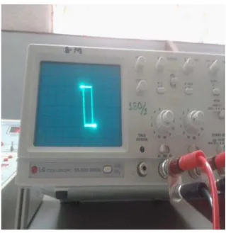
The hysteresis curve is observed on the CRO when the time/ d ivision dia l is kept in X-Y mode. This is illustrated in fig. 8
Fig. 8 Hysteresis curve
4.2 Simulati on Results
The Schmitt trigger circuit using opamp was designed and imple mented using Multisim simu lation package. The simu lation circuit is shown in fig. 9. The waveform for the simulation circuit schematic and the hysteresis curve are shown in fig.10 and 11 respectively
Fig.10 waveforms for the Simu lation circuit
Fig.11 Hysteresis curve for simulation c ircuit.
V.
CONCLUSION
Schmitt trigger c ircuit was designed and imple mented using opamp IC µA-741. The designed system showed excellent characteristics and precise results were obtained. From the results, it can be concluded that a sinusoidal input signal is converted into a rectangular output signal. In other words an Analog signal is converted into a Digital signal. The amp litude of the Rectangular wave was calculated and it was independent of the peak to peak value of the input waveform. The time period and frequency of the rectangular waveform was also calculated. Schmitt trigger c ircuit is very simple and easy to design requiring very few co mponents. Low power consumption is one of the salient features of the system as it uses opamp IC µA-741. Furthermo re, the designed system is very stable, reliable , and easy to use and requires less cost. Due to these advantages it finds use in many applicat ions in diffe rent doma in of electron ics such as Analog to
Dig ital and Dig ital to Analog conversion, level detection and line reception etc.
ACKNOWLEDGEMENT
First of all I would like to thank Almighty Allah by the grace of whom, I reached the stage of complet ion of this work. This avenue has been a turning point in my career to mould me into a thorough professional. My sincere thanks to the principal Dr. S Ka ma l Md Aza m, Vice Principa l Dr. Ruksar Fatima and Dr. As ma Pa rveen H.O.D CSE department of my esteemed institution Khaja Banda Nawa z college of Engineering. I a m also thankful to my be loved parents who have helped me pave this path to success.
REFERENCES
[1] Anil K. Ma ini, Va rsha Agarwal, Electronic Devices and Circuits, (New Delh i: Wiley India Pvt. Ltd.2009), 527-530.
[2] Albert Malvino, David J Bates, Electronic Principles (New Delh i: Tata Mc Gra w Hill, Special Indian edit ion, 2007), 856-859. [3] Donald P. Leach, Alberto Paul Malvino,
Gouta m Saha, Digital principles and applications, (New De lhi: Tata Mc Graw Hill, Special Indian edit ion, 2011), 250-252. [4] A.P. Godse, U.A. Godse, Analog & Digital
Electronics, (Pune: Technical Publications, August 2016), chapter 3,15-30.
[5] Rice. F. Physics 5/105, Introductory Electronics Laboratory, Caltech 2015. [6] Prof. Jun Chen, The Schmitt trigger, Circuits
and systems, ELEC ENG 2CJ4.
[7] Rao Prakash, Pulse and Digital Circuits, (Tata Mc Graw Hill Education, 2006) 267-268.
[8] Jain R.P, Anand M.M.S, Digital electronics practice using Integrated circuit,(Tata Mc Gra w Hill Education, 1983), 158-160.
[9] Otto. H. Sch mitt, A The rmionic trigger, Journal of Scientific instruments, Volu me 15, issue1, January 1938, 24-26.