Low Voltage Analog Circuit Design Based on the
Flipped Voltage Follower
Neeraj Yadav 1, Sanjeev Agrawal 2, Jayesh Rawat 3, Chandan Kumar Jha 4
1, 3, 4Assts. Proff. Techno India NJR Inst. Of Technology Udaipur
2Associate Proff. MNIT Jaipur, MNIT Jaipur
[email protected], [email protected], [email protected], [email protected]
Abstract: The desire for portability of electronics equipment generated a need for low power system in battery products like hearing aids, implantable cardiac pacemakers, cell phones and hand held multimedia terminals. Low voltage analog circuit design differs considerably from those of high voltage analog circuit design. This paper present the basic cell knows as “flipped voltage follower” for low voltage/ low power operation. The detailed classification of basic topologies derived from the FVF cell is presented and there is a low voltage current mirror based on FVF cell has been presented. All the Circuit has been simulated using Hspice tool 0.18µm CMOS Technology. Different quality factors such as frequency response, power consumption are considered. A compression also made between previous current mirror and new designed current mirror. The layout of the current mirror has been also designed using Cadence tool.
Keywords:Analog integrated circuits, low power low voltage design. 1-INTRODUCTION
Downscaling of CMOS process has forced analog circuit to operate with continuously decreasing supply voltage. Downscaling of CMOS has been mainly due to need of reduced power consumption of the digital circuitry in mixed mode very large scale integration (VLSI) system and to prevent oxide breakdown with decreasing gate oxide thickness.
In addition portable electronic equipments are based on the low power consumption and low supply voltage. Several technique have been presented to reduce supply voltage requirement in analog and mixed signals circuits, among them folding triode mode and sub threshold operation of MOS transistor, folding gate techniques and current mode processing [1].
2. Voltage Follower
A basic cell called voltage follower or voltage buffer used for low voltage analog circuit design. A basic cell for low voltage/ low power is identified. Let us consider the common drain amplifier frequently used as a voltage buffer. If body effect is ignored the circuit follows the input voltage with a dc shift i.e. Vo= Vi+ Vsgm1 where Vsgm1 is the
source-to-gate voltage of transistor M1.
There are some drawback of the voltage follower, in many applications the output resistance is not enough low. It can be only be decreased by increasing the Trans conductance gain gm. this require a large current biasing and large
Figure 1 Voltage Follower
The gate source voltage of M1 varies with the input signal, this leads to distortion that increase at high frequency. The slew rate is nonsymmetrical since the sourcing capability is very large, while the sinking capability is limited by the bias current Ib.
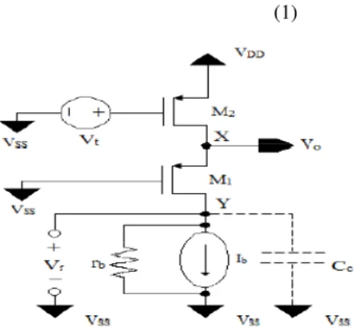
3. Flipped Voltage Follower
It is essentially a cascade amplifier with negative feedback where the gate terminal of M1 is used as input terminal and its source as output terminal. It is characterized by very low output impedance due to shunt feedback provided by M2, high low supply requirement close to a transistor threshold voltage VTH, low static power dissipation and high
gain bandwidth. The name flipped voltage follower is based on the fact that FVF is biased on the drain side rather than the source side.Output current variation are absorbed by M2 which is denoted current sensing transistor, while
the current in M1 remain constant, due to this the gate source voltage of M1 remain constant and distortion remain low
even at higher frequency. A practical limitation of the FVF cell is that it gives very small input and output signal swing.
Figure 2 Flipped Voltage Follower
The circuit in Figure 2 is another voltage follower where the current through transistor M1 is held constant, independent on the output current. It could be described as a voltage follower with shunt feedback. Neglecting the short-channel effect, Vsg1 is held constant, and voltage gains are unity.
3.1. Resistance Estimation of The FVF Cell 3.1.1. Resistance at node Y:
= + + (1)
Figure 3 Open- loop gain analysis of FVF cell
−
+ = +
Vgs1=Vg1-Vs1 and Vgs2=Vg2-Vs2
From eq. 1 we get
− − = (2)
= + + (3 )
Figure 4 Small signal diagram of open loop gain analysis of FVF cell for node y
Substituting the value of Vs1 from eq. 3 and rearranging
= ||( + + ) (4)
Using approximation
gm1ro1>1 (5)
gm1r02>1 = ||
The resistance at node x can be determined by the small signal analysis of open loop gain analysis of FVF cell. Small signal diagram of open loop gain analysis of FVF cell for node x is shown in figure 3.7
"= "+ "+ # "− $% (6)
"+ # "− $% = $ (7)
Figure 5 Small Signal diagram of open-loop gain analysis of FVF cell for node x
Rearranging the equation
" " =
(1 + * ( 1 )
(1 + 1 + 1/ (8)
Using the approximation
= ||(1 + * (9)
Open loop gain is .
/ 0. 2. (3 )
4= − ( 250567892 08 : 708) = − ( ;) Using gain of the common gate amplifier i.e.
<=
( + 1)
+ + ; + (11) Using equation and two approximations we get
<=
( + 1)
+ + + = − +
= − ( || ) = −
= 4=1 + |3 | =4
||(1 + )
1 + ( || )
= ||(
1 + )
( || )
It is observed that RCLX is very low resistance.
Note that FVF can operate at a very low voltage supply, and that it is the operating condition we are interested in. By the analysis we get the valid range of operation for the input signal
$$− (| >?| − | >?| − @ 2
AB(CD) < F < $$− (| >?| − @
2
AB(GD ) − @
2 AB(GD )
(12)
It is clear that the valid input signal range reduces with the transistor threshold voltage, which limits the applications of the FVF in deep submicron technologies.
4. Basic FVF Structures 4.1. FVF current sensors (FVFCS)
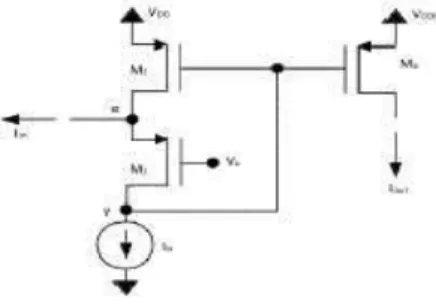
The FVF cell can also considered to as a current sensing cell, and when used in this way it will be called a “FVF current sensor (FVFCS).” Let us consider node in Fig. 6 as the input current sensing node and that all transistors are properly biased to work in the saturation region. Due to the shunt feedback provided by transistor M2, the impedance
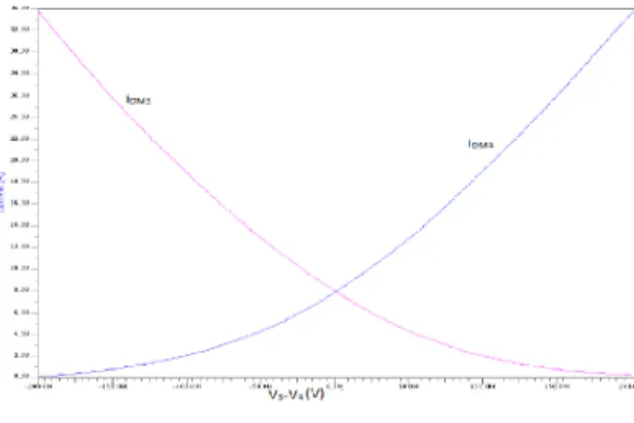
at node x is very low and, this way, the amount of current that flows through this node does not modify the value of its voltage. Note that node x can source large current variations at the input and the FVF translates them into compressed voltage variations at output node .This voltage can be used to generate replicas of the input current as shown in Fig. 6 by means of transistor M5 . Fig. 7 shows the dc response of the circuit in Fig. 7. The output and the input currents are related through the expression Iout = Iin +Ib . The current can be easily removed from the output node
using current mirroring techniques if this is needed for a specific application.
Figure 6 FVF Current sensor
Apart from this particular operating condition, the FVFCS can be operated with very low voltage supply. The minimum supply voltage is $$<H = | >?| + 2 $ IF ; where |VTP| is the transistor threshold voltage and VDSsat is the
Figure 7 DC response of the FVFCS Structure
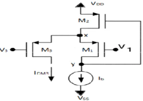
4.2 FVF differential structure (DFVF)
The first differential structure based on the FVF cell can be built by adding an extra transistor connected to node x , as it is shown in Fig. 8 [1]. This structure called the “FVF differential structure (DFVF).” As indicated in the previous section, the impedance at node x is very low and its voltage remains approximately constant for large currents through transistor M3 . If we consider quiescent conditions when V1 =V3 , and assuming the same transistor
sizes for M1 and M3 , the condition IDM1 = IDM3 = Ib is satisfied. Differential voltage V1 -V3 generates current
variations in M3 that follow the MOS square law. This is a very interesting property of the DFVF as the maximum
output current can be much larger than the quiescent current Ib . Fig. 9 shows the dc transfer.
Figure 8 Differential Flipped Voltage Follower
Another characteristic of the DFVF is that the output is available as both a current (IDM3, or the current through
transistor M2 replicated by means of a current mirror), and a voltage (node y ). This feature can be advantageously
employed to simplify the circuit implementations reducing both noise and number of poles and zeros. Finally, the DFVF can also be operated with very low supply voltage. The minimum supply voltage is, as in the case of the FVFCS $$<H= | >?| + 2 $J IF,. Once again, with a supply of VMIN DD there would be no room for variation of the input signals V1 and V3. It is easy to obtain an expression relating the expected variation of V1 and V3 with the
Figure 9 DC Response of the DFVF cell
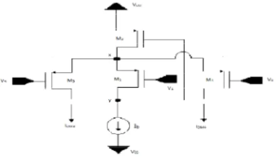
4.3 FVF pseudo-differential pair cell (FVFDP):
A FVFDP structure can be easily constructed by adding an extra transistor M4 at node x in DFVF structure, as
shown in Fig. 10. This structure is known as “FVF pseudo differential pair (FVFDP).” Fig. 11 shows the dc output currents IDM3 IDM4 versus the differential input voltage V3-V4, in a typical case. The pseudo-differential pair also
exemplifies the characteristic behaviour of a Class-AB circuit, where the quiescent output current Ib can be much
lower than the peak value. In this case, we have considered that, under quiescent conditions, V1 =V3 =V4. That is,
assuming perfect matching between transistors M1 ,M3 and M4, the voltage at the gate of corresponds to the common
mode of M3 and M4: = KLM=VCMi. If the common-mode value VCMi of input voltages V3 and V4 is not equal to 1V
the dc output characteristic has the same shape, but a dc level shift is applied to the curves of transistor currents in opposite directions of the horizontal axis.
Figure 10 Basic FVFDP Structure
The main difference between the DFVF and the FVFDP is that the latter has a true differential output. The output current of the DFVF can be large if V1 –V3 is positive and zero if V1 –V3 is negative, while in the FVFDP we can
have positive or negative large differential output currents (Iout = IDM3 –IDM4) depending on the value of the input
differential voltage (Vin = V3 –V4) . This pseudo-differential pair can be also operated with a minimum supply
Figure 11 DC Response of the FVFDP structure
5. APPLICATIONS OF THE FVF CELL 5.1 Current Mirror
5.1.1 General properties
A current mirror is an element with at least three terminals. The common terminal is connected to a power supply, and the input current source is connected to the input terminal. Ideally, the output current is equal to the input current multiplied by a desired current gain. If the gain is unity the input current is reflected to the output, leading to the name current mirror. Under ideal condition the current mirror gain is independent of input frequency, and the output current is independent of the voltage between the output and common terminals.
Figure 12 Current mirror block diagrams referenced to (a) ground and (b) the positive supply.
5.1.2 Low –Voltage Current Mirror Based On the Flipped –Voltage Follower
The well known flipped voltage follower (FVF) cell has been employed for realizing low voltage current mirrors. The minimum supply voltage requirement for the correct operation of the current mirror is equal to VTH+VDS, sat ,
making all of them compatible with the minimum power supply voltage requirement of the modern signal processing systems [J. Ramirez-Angulo, R.G. Carvajal., A. Torralba, J. Galan. A.P. Vega-Leal, J. Tombs, 2002].
Figure13 Conventional cascade current mirror
With regards to the voltage restriction the minimum supply requirement is given by
$$, <H= >O(P )+ $J, IF(PQ) (12)
Where VTH(M1) is the threshold voltage of the M1 and VDS, sat(M1) is the saturation voltage of the M7 . Other
important factors that establish the capability of the current mirror in Figure 3.4 to operate in a low voltage environment are the minimum input and output voltages [8]. The corresponding expression are given by (13) and (14), respectively
<H= >O(P ) (13)
RF <H = $J, IF(P )+ $J, IF(PS) (14)
The input and output resistance of the current mirror in figure are given by
<H=
1
(P )
(15)
RF= (PS). (P ). (PS) (16)
An alternative topology of that shown in figure is based on the adaptive bias scheme given in Figure
Figure14 Cascade current mirror with adaptive bias scheme.
Another current mirror configuration that is widely used in low-voltage applications is that depicted in Figure 3.6. This is a cascode current mirror based on the FVF cell. The minimum required supply voltage and the minimum input voltage are also given by (1) and (2), while the minimum output voltage and output resistance are now [5]
RF= $J, IF(P )+ $J, IF(PS) (16)
Figure 15
6. Simulation Results 6.1 Simulation result for voltage follower:
The circuit for the voltage follower shown in figure is simulated using the Hspice tool for 0.18µm CMOS technology. Different parameters and dimensions used in circuit simulation are shown in the table. The value of the bias voltage (Vb), the input voltage (Vi), supply voltage (VDD) and source voltage (VSS) are chosen as 0.35V, 0,25V,
0.9V and 0V respectively.
Table1 Transistor dimension for the voltage follower
Transistor W[µm] L[µm]
M1 16 0.2
M2 14 0.2
Figure16 DC transfer characteristics of voltage follower
Figure 17.Frequency response of the voltage follower
6.2 Layout of the voltage follower:
Layout of the voltage follower cell has been simulated using Cadance (virtuoso) for 0.18µm CMOS technology. The design rule check (DRC), layout versus schematic (LVS) done using Cadance. Shown in the figure 18
Figure 18.Layout of the voltage follower
6.3 Simulation Result for the Flipped Voltage Follower:
The circuit for the flipped voltage follower is shown in the figure is simulated using Hspice tool 0.18µm CMOS technology. Different parameter used for the simulation is given below and the dimension of the transistor is shown in the table. The bias voltage (Vb), input voltage (Vin) supply voltage (VDD) and the source voltage (VSS) are given as
0.7V, 0.12V, 0.9V and 0V respectively.
Table2 Dimension of the flipped voltage follower
Transistor W[µm] L[µm]
M1 100 2
M2 18.1 2
M3 0.5 0.5
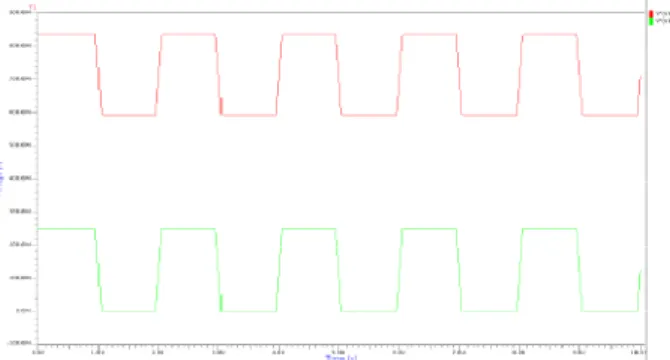
The DC transfer characteristics of the flipped voltage follower are shown in the figure 19. Hera the input varies from 0V to 0.4V with the increment of the 0.001V.Here the output varies linearly with the input voltage. The transient analysis of the voltage follower is also shown in the figure 20.Frequency response of the flipped voltage follower is also shown in the figure 21.The total power consumption is the 7.109mm.
Figure 20 Transient analysis of the flipped voltage follower
Figure 21.Frequency response of the flipped voltage follower
6.4 Layout for flipped voltage follower:
Layout of the flipped voltage follower cell has been simulated using Cadance (virtuoso) for 0.18m CMOS technology. Layout diagram of the current mirror is shown in the figure22. The design rule check (DRC), layout versus schematic (LVS) done using Cadance.
Figure 22.Layout of the Flipped Voltage Follower
6.5 Simulation result for cascode current mirror
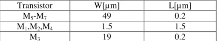
Transistor W[µm] L[µm]
M5-M7 49 0.2
M1,M2,M4 1.5 1.5
M3 19 0.2
The frequency response of cascode current mirror is shown in Figure 23. From Figure, it can be seen that the bandwidth is less than 100 MHz with load capacitance CL = 500 fF. The105.9356 µW.
Figure 23 Frequency response of cascode current mirror
Comparative results of the simulated performances between designed cascode current mirror and cascode current mirror in [8] are shown in Table 4
Table4 Comparison of simulated performance between the designed cascode current mirror and cascode current mirror in [8].
Performance factor Designed Cascode Current Mirror Cascode Current Mirror [C. Koliopoulos, C. Psychalinos] 2007 Technology used (m)
0.18 0.18
Supply Voltage 1.5 1.5
DC power dissipation (w)
102.93 217
Cutt-off frequency (MHz)
<100 133
6.6 Simulation Result For Cascode current mirror with adaptive bias scheme
The circuit of cascode current mirror with adaptive bias scheme, shown in Figure 13, has been simulated using tool Hspice for 0.18 µm CMOS technology. The transistor dimensions are listed in Table 3. The values of bias voltage (VBIAS ), supply voltage (VDD) and source voltage ( VSS ) are chosen as 0.98 V, 1.5 V and 0 V respectively. The frequency response of cascode current mirror with adaptive bias scheme is shown in Figure 24. From Figure, it can be seen that the bandwidth is over 100 MHz with load capacitance CL=500fF.The total power consumption of cascode
current mirror with adaptive bias scheme is 185.53 µW.
Table5.Transistor dimensions of cascode current mirror with adaptive bias scheme.
Transistor W[µm] L[µm]
M6-M9 49 0.2
M1,M2,M3,M5 1.5 1.5
M4 19 0.2
Table6. Comparison of simulated performance between the designed cascode current mirror with adaptive bias scheme and cascode current mirror with adaptive bias scheme in [8]
Performance factor Designed cascade current mirror based on adaptive
bias scheme
Cascade current mirror with adaptive bias
scheme [C. Koliopoulos, C. Psychalinos]2007. Technology used
(m)
0.18 0.18
Supply voltage (V) 1.5 1.5
DC power dissipation (w)
185.53 289
Cut-off frequency (MHz)
100 81
Figure 24 Frequency response of cascode current mirror with adaptive bias scheme
6.7 Simulation Result For Current mirror based on FVF cell
The circuit of current mirror based on FVF cell, shown in Figure 4, has been simulated using tool Hspice for 0.18
µm CMOS technology. The transistor dimensions are listed in Table 5. The values of bias voltage (VBIAS) , supply voltage ( VDD) and source voltage ( VSS) are chosen as 0.98 V, 1.5 V and 0 V respectively.
The frequency response of the current mirror based on FVF cell is shown in Figure 6. From Figure 3.9, it can be seen that the bandwidth is over 1000 MHz with load capacitance CL =500fF. The total power consumption of FVF
cell based current mirror is 107.01 µW.
Table7. Transistor dimensions of current mirror based on FVF cell.
Transistor W[m] L[m]
M-M 49 0.2
M1,M2,M4 1.5 1.5
Figure 25 Frequency response of current mirror based on FVF cell
Table8. Comparison of simulated performance between the designed current mirrors with adaptive bias scheme and cascode current mirror with adaptive bias scheme in [8]
Performance factor Designed current mirror based on FVF cell
Current mirror based on FVF cell [C. Koliopoulos, C. Psychalinos] 2007 Technology used (µm)
Supply voltage (V) 1.5 1.5
DC power dissipation (µW) 185.53 218
Cut-off frequency (MHz) 1000 212
6.8 Layout of current mirror based on FVF cell
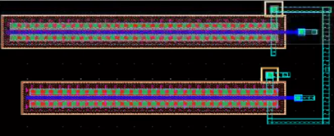
Layout of current mirror based on FVF cell has been designed using tool IC Station Editor (Mentor Graphics) for tsmc 0.18 µm CMOS technology libraries. Layout diagram of current mirror based on FVF cell is shown in Figure 3.10. The design rule check (DRC), layout versus schematic (LVS) and post extraction (PEX) checking has also been performed using tool Calibre (Mentor Graphics).
Figure 26 Layout of Current Mirror based on the FVF cell
7. Conclusion
This paper is based on the flipped voltage follower which is used for the designing of the low voltage low power analog circuit design. In this paper I have discussed different structure and the applications of the flipped voltage follower. The power consumption and the different analysis is done using Cadence tool, and the layout of the voltage follower and the flipped voltage follower is presented. There is made a comparison between the current mirror which is designed in this paper and the current mirrors which has been presented in the previous paper.
REFERENCES
[2] S.S. rajput and S.S. Jamuar, “Design Techniques for low voltage Analog circuit structures,” NSM 2001/IEEE 2001 page 24-42.
[3] J.Pan, Y.Inoue, and Z Liang, “An energy management circuit or self powered ubiqitions sensors modulesuing vibration-based energy ”.
IEICE trans fundamental vol.E90-A no.10 pp 2116-2123, oct 2007.
[4] J. Ramirez-Angulo, R.G. Carvajal., A. Torralba, J. Galan. A.P. Vega-Leal, J. Tombs, “The flipped voltage follower: a useful cell for low-voltage low-power circuit design,” Circuits and Systems, 2002. ISCAS 2002. IEEE International Symposium on, Volume 3, pp. 615 – 618, 26-29 May 2002.
[5] M.Wilamowski Bogdan, “VLSI Analog Multiplier/divider Circuit,” International Symposium on Industrial Electronics, Pretoria, South Africa, pp. 493-496, July 7- 10, 1998.
[6] Eric A. Vittoz, “Analog VLSI signal processing: Why, where and how?”, International Journal on Analog Integrated Circuits and Signal Processing, Vol. 6, No. 1, pp. 27-44, July, 1994,.
[7] S. Yan and E. Sánchez-Sinencio, “Low voltage analog circuit design techniques: IEICE Trans. Fund., vol. E83, no. 2, pp. 1–17, Feb. 2000.
[8] C. Koliopoulos, C. Psychalinos, “A Comparative Study of the Performance of the Flipped Voltage Follower Based Low-Voltage Current Mirrors,” Signals, Circuits and Systems, 2007. ISSCS 2007. International Symposium on Volume 42, pp. 1- 413-14, July 2007.
[9] Behzad Razavi, “Design of Analog CMOS Integrated Circuits”, Tata McGraw- Hill pp. 67-75, 2002. A tutorial,” IEICE Trans. Fund., vol. E83, no. 2, pp. 1–17, Feb. 2000.
[10] S. Soclof, Applications of Analog Integrated Circuits, Prentice Hall, 1985.
[11] R. Jacob Baker, Harry W. Li and David E. Boyce, CMOS Circuit Design, Layout and Simulation, Prentice Hall, 1998. [12] D.P.Stokesderry “A Large signal IGFET dc source follower” Procedding of the IEEE pp. 66 November 12 1965.
[13] Suming Lai; Hong Zhang; Guican Chen; Jianchao Xu; “An improved source follower with wide swing and low output impedance” Circuits and Systems, 2008. APCCAS 2008. IEEE Asia Pacific Conference pp. 814-817 2008.
[14] Ramón González Carvajal, Senior Member, IEEE, Jaime Ramírez-Angulo, Fellow, IEEE, Antonio J. López-Martín, Member, IEEE, Antonio Torralba, Senior Member, IEEE, Juan Antonio Gómez Galán, Alfonso Carlosena, Member, IEEE, and Fernando Muñoz Chavero “The Flipped Voltage Follower: A Useful Cell for Low-Voltage Low-Power Circuit Design” IEEE TRANSACTIONS ON CIRCUITS AND SYSTEMS—I: REGULAR PAPERS, VOL. 52, NO. 7, JULY 2005
[15] “A four quadrent analog multiplier ” Solid state circuit conference 1985 ESSCIRC 85 pp.16-18 sept.1985. [16] “A GaAs four quadrant analog multiplier circuit” solid state circuit IEEE Journal of March 1989 pp. 388.