Low Voltage Analog Circuit Design Based on the Flipped Voltage Follower
Texto
Imagem


Documentos relacionados
Este relatório pretende descrever o modo como estas três áreas (modelo de jogo, modelo de treino e modelo de análise do jogo) foram concebidas e operacionali- zadas ao longo de
The radargram obtained with the application of the 400 Mhz antenna in area 2 is shown in Figure 9 , where it can be verified that the distance reached by the signal achieved a
Figure 2 shows a block diagram of the RF generator board with the corresponding voltage and current measurement stages. The circuit is composed of: 1) astable oscillator adjusted
The circuit shown in Figure 5b has a symmetric topology of two Wilson current mirrors to generate biphasic pulses with output current that is independent of load.. The use of
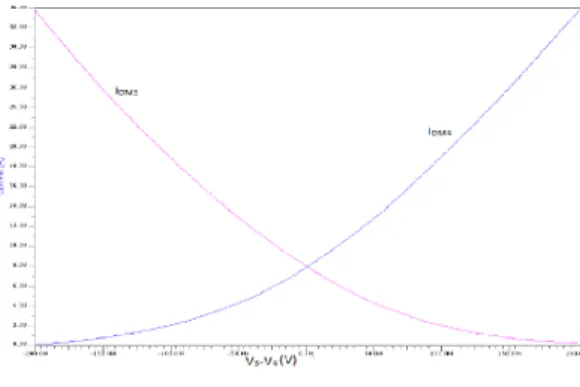
Abstract — A new current-mode squaring circuit that can be used as a basic building block in analog signal processing systems is proposed.. The design is based on
Simulation circuit of WECS with PMSG using Fuzzy Logic controller is shown in the Figure 12 .The output voltage for Buck Boost Converter and SPWM based inverter is
The curve of voltage generated and delivered to a resistive load during the generation can be seen through figure 8(c), and in the figure 8(d), the curve of voltage in one of the
Furthermore, the legal documents characterizing and transforming these forest regimes are also included as are all concrete cases that directly and explicitly affect firms or
