Roman Vladimirovitch Kliko
Licenciatura em Ciências da Engenharia Electrotécnica e de Computadores
Design of a Digital Temperature Sensor
based on Thermal Diffusivity in a
Nanoscale CMOS Technology
Dissertação para obtenção do Grau de Mestre em Engenharia Electrotécnica e de Computadores
Orientador: João Carlos da Palma Goes, Professor Associado
com Agregação, FCT-UNL
Júri:
Presidente: Prof. Doutor Luís Filipe Figueira de Brito Palma Arguente: Prof. Doutor Luís Augusto Bica Gomes de Oliveira Vogal: Prof. Doutor João Carlos da Palma Goes
iii
Design of a Digital Temperature Sensor based on Thermal Diffusivity in a Nanoscale CMOS Technology
Copyright © Roman Vladimirovitch Kliko, Faculdade de Ciências e Tecnologia, Universidade Nova De Lisboa
A Faculdade de Ciências e Tecnologia e a Universidade Nova de Lisboa têm o direito, perpétuo e sem limites geográficos, de arquivar e publicar essa dissertação através de exemplares impressos reproduzidos em papel ou de forma digital, ou por qualquer outro meio conhecido ou que venha a ser inventado, e de a divulgar através de repositórios científicos e de admitir a sua cópia e distribuição com objectivos educacionais ou de investigação, não comerciais, desde que seja dado crédito ao autor e editor.
v
Acknowledgements
I would like to show my graditude to the Department of Electrical Engineering of the Faculty of Science and Technology for providing me a stimulant and challenging working environment and friendly atmosphere that made me work better, for providing the necessary means, and for its high institutional standards.
I would like to thank Professor João Goes, my thesis advisor, which proved to be always available to explain doubts about the work/project, and demonstrated patience, stimulating suggestions, dedication, and constant encouragement.
I would also like to thank to various people that helped me in the development of this thesis with important advices at different levels.
I also must to thank to all my friends and colleagues that interacted with me, who have been available in several crucial moments, and provided fun times and entertaining experiences over the years.
vii
Universidade Nova de Lisboa
Resumo
Faculdade de Ciências e Tecnologia
Departamento de Engenharia Electrotécnica e de Computadores
Dissertação para obtenção do grau de Mestre em Engenharia Electrotécnica e de Computadores
por Roman Kliko
Sensores de temperatura são amplamente utilizados em microprocessadores para monitorizar gradientes de temperatura ‘on-chip’ e 'hot-spots', que são conhecidos por afectar negativamente a fiabilidade. Estes sensores devem ser pequenos, por razões de incorporação no circuito integrado do sistema, rápidos em detectar alterações térmicas transitórias em fracções de segundos, e de fácil ajuste para reduzir custos associados. Recentemente, foi demonstrado que sensores de difusividade térmica (TD) conseguem satisfazer esses requisitos. Esses sensores operam através da digitalização do atraso, dependente da temperatura, associado com a difusão de pulsos de calor através de um filtro electrotérmico (ETF), que, em tecnologia CMOS padrão, podem ser facilmente implementados como aquecedor resistivo cercado por uma termopilha. Ao contrário dos sensores de temperatura baseados em BJTs, as suas precisões na realidade melhoram com o escalamento dos transístores nas tecnologias CMOS, uma vez que é principalmente limitado pela precisão do espaçamento do aquecedor/termopilha.
Neste trabalho é apresentado um sensor TD altamente digitalizado em tecnologia CMOS de 0.13 µm com ±1.5 ºC (3σ, ajuste único) de imprecisão e alcançando uma resolução melhor
do que 1 ºC a uma taxa de amostragem da ordem de 1 kS/s, e que se compara favoravelmente
aos sensores de última geração com precisão similar e taxas de amostragem [1][2][3][4]. Este avanço é alcançado nomeadamente pela adoção de uma arquitectura de modulação ΣΔ, altamente digital, baseado num oscilador controlado por corrente (CCO).O sensor TD apresentado consiste num ETF, num andar de trasnconductância, num oscilador controlado por corrente (CCO) e num contador digital de 6 bits.
De modo a ser facilmente portado para tecnologias CMOS de escala nanométrica, é proposto usar um modulador sigma-delta baseado num CCO como uma alternativa aos moduladores tradicionais. Dado que 70% da área do sensor é ocupada por circuitos puramente digitais, portar o sensor para tecnologia CMOS de última geração deve reduzir substancialmente a área digital, e assim reduzir significativamente a área total do sensor.
viii
Palavras-Chave: Sensor de Temperatura Digital, Difusividade Térmica, Gestão Térmica Dinâ- mica, Filtro Electrotérmico, Modulação Sigma-Delta, Oscilador Controlado por Corrente.
ix
Universidade Nova de Lisboa
Abstract
Faculdade de Ciências e Tecnologia
Departamento de Engenharia Electrotécnica e de Computadores
Dissertação para obtenção do grau de Mestre em Engenharia Electrotécnica e de Computadores
by Roman Kliko
Temperature sensors are widely used in microprocessors to monitor on-chip temperature gradients and hot-spots, which are known to negatively impact reliability. Such sensors should be small to facilitate floor planning, fast to track millisecond thermal transients, and easy to trim to reduce the associated costs. Recently, it has been shown that thermal diffusivity (TD) sensors can meet these requirements. These sensors operate by digitalizing the temperature-dependent delay associated with the diffusion of heat pulses through an electro-thermal filter (ETF), which, in standard CMOS, can be readily implemented as a resistive heater surrounded by a thermopile. Unlike BJT-based temperature sensors, their accuracy actually improves with CMOS scaling, since it is mainly limited by the accuracy of the heather/thermopile spacing.
In this work is presented the electrical design of an highly digital TD sensor in 0.13
µm CMOS
with an accuracy better than 1 ºC resolution at with 1 kS/s sampling rate, and which compares favourably to state-of-the-art sensors with similar accuracy and sampling rates [1][2][3][4]. This advance is mainly enabled by the adoption of a highly digital CCO-based phase-domain ΔΣ ADC.The TD sensor presented consists of an ETF, a transconductance stage, a current-controlled
oscillator (CCO) and a 6 bit digital counter.In order to be easily ported to nanoscale CMOS technologies, it is proposed to use a sigma-delta modulator based on a CCO as an alternative to traditional modulators. And since 70% of the sensor’s area is occupied by digital circuitry, porting the sensor to latest CMOS technologies process should reduce substantially the occupied die area, and thus reduce significantly the total sensor area.
Keywords: Digital Temperature Sensor, Thermal Diffusivity, Dynamic Thermal Management, Electro-thermal Filter, Sigma-Delta Modulation, Current-Controlled Oscillator.
xi
Contents
Acknowledgements ... v
Resumo ... vii
Abstract ... ix
List of figures ... xiii
List of tables ... xv
Acronyms and Abbreviations ...xvii
1. Introduction ... 1
1.1. Background and Motivation ... 1
1.2. Main Objectives ... 3
1.3. Thesis Outline ... 4
1.4. Thesis Contributions ... 5
2. State-of-the-Art of Temperature Sensors ... 7
2.1. Sensor types ... 7
2.1.1. Sensors based on PNP Devices ... 7
2.1.2. Sensors based on NPN Devices ... 8
2.1.3. Standard BJT Sensors ... 8
2.1.4. Temperature Sensors based on Thermal diffusivity ... 9
2.1.5. Results comparison ... 10
3. Design of the Main Building-Blocks... 11
3.1. Flip-Flops ... 12
3.1.1. D Flip-Flop ... 12
3.1.2. JK Flip-Flop ... 15
3.2. The Digital Counter ... 15
3.2.1. Synchronous 6-bit Up/Down Binary Counter ... 16
3.3. Controlled Oscillators ... 17
3.3.1. Oscillator 1 (CCO 1) ... 20
3.3.2. Oscillator 2 (CCO 2) ... 21
3.4. Transconductance Stage (gm) ... 23
3.5. Digital-to-Analog Converter ... 24
3.5.1. The 6 bit IDAC ... 27
xii
4. Design Methodology and Sizing ... 35
4.1. Digital Part ... 35
4.2. Analog Circuitry ... 35
4.2.1. Oscillator 1 (CCO 1) ... 36
4.2.2. Oscillator 2 (CCO 2) ... 36
4.2.3. Transconductance Stage (gm) ... 37
4.2.4. Electro-Thermal Filter (ETF) ... 39
4.2.5. The 6 bit IDAC ... 40
5. Simulation Results... 43
5.1. Flip-Flops ... 43
5.1.1. D Flip-Flop ... 43
5.1.2. JK Flip-Flop ... 44
5.2. The Digital Counter ... 45
5.2.1. Synchronous 6-bit Up/Down Binary Counter ... 45
5.3. Oscillators ... 47 5.3.1. Oscillator 1 (CCO 1) ... 47 5.3.2. Oscillator 2 (CCO 2) ... 49 5.3.3. Conclusion of oscillators ... 52 5.4. Transconductance Stage (gm) ... 52 5.5. Digital-to-Analog Converter ... 52
5.5.1. The 6 bit IDAC ... 52
5.6. Electro-Thermal Filter (ETF) ... 53
5.7. TDT Sensor – Open Loop ... 55
5.7.1. Interconnecting the Transconductance stage and the Oscillator (CCO 1) ... 55
5.7.2. Interconnecting the transconductance stage, the Oscillator (CCO 1) and the 6 bit counter……….………..56
5.7.3. Interconnecting the ETF, the transconductance stage, the Oscillator (CCO 1), the 6 bit counter and the two backend D Flip-Flops………....57
5.8. TDT Sensor – Closed Loop Simulations ... 59
5.8.1. Complete Schematic of TDT Sensor ... 60
6. Conclusions and Future Work ... 63
6.1. Conclusions ... 63
6.2. Future Work ... 64
xiii
List of Figures
Figure 1.1 - Block diagram of the proposed thermal diffusivity temperature sensor with a CCO-
-based phase-domain ΔΣ modulator, and the corresponding timing diagram………..2
Figure 1.2 – Lateral view of an Electrothermal Filter (ETF) in bulk CMOS technology ... 3
Figure 3.1 - Block diagram of the proposed thermal diffusivity temperature sensor with a CCO- -based phase-domain ΔΣ modulator, and the corresponding timing diagram……..11
Figure 3.2 – Logic symbol for edge-triggered negative D flip-flop ... 13
Figure 3.3 – Circuit schematic of a master-slave negative edge-triggered D flip-flop ... 13
Figure 3.4 – Representation of a master-slave negative edge-triggered D flip-flop ... 14
Figure 3.5 – Representation of a master-slave positive edge-triggered D flip-flop ... 14
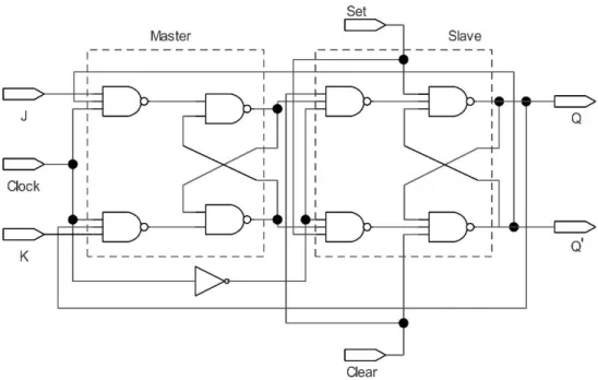
Figure 3.6 – Circuit schematic of master-slave negative JK Flip-Flop with set and clear ... 15
Figure 3.7 – Circuit schematic of synchronous 6 bit up/down binary counter ... 17
Figure 3.8 – Closed-loop circuit model of basic feedback oscillator configuration... 18
Figure 3.9 – Circuit schematic of oscillator 1 (CCO 1) based on a ring-oscillator configuration .... 21
Figure 3.10 – Circuit schematic of oscillator 2 (CCO 2) ... 22
Figure 3.11 – Digital-analog converter (DAC) in applications of signal-processing ... 25
Figure 3.12 – Ideal characteristics of input-output for 3-bit DAC ... 26
Figure 3.13 – Simplifier circuit schematic of 6 bit IDAC ... 28
Figure 3.14 – Simple binary weighted current steering DAC and its implementation with transis- tors……….……29
Figure 3.15 – Diffusion of temperature sensors and micro heaters on a silicon substrate ... 31
Figure 3.16 – Side view of a silicon slab ... 31
Figure 3.17 – Vibrational mode of phonons ... 32
Figure 3.18 – Simplified schematic layout (a), and photomicrograph (b) of the optimized CMOS ETF ………33
Figure 3.19 – A streamlined cross section of an ETF in standard CMOS ... 33
Figure 4.1 – Transistor sizing of oscillator 2... 36
Figure 4.2 – Circuit schematic of differential pair and 6 bit IDAC, constituting gm stage ... 38
xiv
Figure 4.4 – Circuit schematic of 6 bit IDAC´s unit device ... 40
Figure 5.1 – Timing diagram of master-slave negative edge-triggered D flip-flop ... 44
Figure 5.2 – Timing diagram of master-slave negative JK flip-flop with set and clear always on ……….44
Figure 5.3 – Timing diagram of master-slave negative JK flip-flop with set and clear……...….45
Figure 5.4 – Timing diagram of synchronous 6-bit up/down binary counter regarding Set and Cle- ar inputs ... 46
Figure 5.5 – Timing diagram of synchronous 6-bit up/down binary counter regarding Up/Down input ... 46
Figure 5.6 – Evolution of frequency versus the input current variation (C = 1 pF) for oscillator 1.. 47
Figure 5.7 – Variation of frequency versus input current (C = 500 fF) for oscillator 1 ... 47
Figure 5.8 – Variation of frequency with the input current (C = 100 fF) for oscillator 1 ... 48
Figure 5.9 – Transient oscillation in the simulation run of oscillator 1 ... 49
Figure 5.10 – Variation of frequency with current (C = 1 pF) for oscillator 2 ... 50
Figure 5.11 – Variation of frequency with the input current (C = 500 fF) for oscillator 2 ... 50
Figure 5.12 – Variation of frequency with current (C = 100 fF) for oscillator 2 ... 51
Figure 5.13 – Transient oscillation in the simulation run of oscillator 2 ... 51
Figure 5.14 – Simulated output voltage of the 6 bit IDAC ... 53
Figure 5.15 – Behaviour of ETF, between input and output waves, for phase shift of 0º ... 53
Figure 5.16 – Behaviour of ETF, between input and output waves, for phase shift of 45º ... 54
Figure 5.17 – Response of the ETF in terms of phase-shift, with resistance variation ... 54
Figure 5.18 – Behaviour of differential pair and oscillator ... 55
Figure 5.19 – Simulated behaviour of the transconductance stage, oscillator and 6 bit counter ... 57
Figure 5.20 – Simulated behaviour of ETF (phase shift = 45º), differential pair, oscillator, 6 bit counter and two D flip-flops ... 58
Figure 5.21 – Circuit schematic of the complete TDT Sensor System ... 59
Figure 5.22 – Simulated behaviour of the complete circuit of TDT Sensor in closed-loop confi- guration ... 61
Figure 5.23 – Simulated FFT of the phase-domain ΔΣ modulator bitstream during fine conversion with 15000 samples ... 62
xv
List of Tables
Table 2.1 – Performance summary and comparison with other state-of-the-art sensors reported in
the literature... 10
Table 3.1 – Truth table of a master-slave negative edge-triggered D flip-flop ... 14
Table 4.1 – Size of all transistors used in the transconductance stage ... 39
Table 4.2 – Width dimensions of the six binary-weighted current-sources ... 41
Table 5.1 – Amplitude response with current variation in oscillator 1 ... 48
Table 5.2 –DC operating point of all transistors of the transconductance stage ... 52
xvii
Acronyms and Abbreviations
TD Thermal Diffusivity
TDT Thermal Diffusivity Temperature TDC Temperature-to-Digital Converter ETF Electro-Thermal Filter
VCO Voltage-Controlled Oscillator CCO Current-Controlled Oscillator
CMOS Complementary Metal-Oxide-Semiconductor BJT Bipolar Junction Transistor
NPN Negative Positive Negative PNP Positive Negative Positive ADC Analog-to-Digital Converter DAC Digital-to-Analog Converter DTM Dynamic Thermal Management
MOSFET Metal Oxide Semiconductor Field Effect Transistor DC Direct Current
FET Field-Effect Transistor YIT Yttrium Iron Garnet SAW Surface Acoustic Wave MSB Most Significant Bit LSB Least Significant Bit FSR Full Scale Range SOI Silicon On Insulator DEM Dynamic Element Matching SAR Successive Approximation Register RFID Radio Frequency IDentification CDS Correlated Double Sampling
1
Introduction
1
1.1. Background and Motivation
Temperature sensors are broadly used in microprocessors to control on-chip temperature gradients and hot-spots, known to negatively impact reliability [1][2][3][4]. With microprocessors scaling to higher performance and faster speed, heat dissipation has become a growing concern. Excessive heat degrades performance and increases power dissipation of the entire system [6]. When microprocessors getting hot, the cooling system must handle worst-case workloads, having as solution, dynamic thermal management (DTM), which enables dynamically balanced workload, the cooling system only has to handle average workloads, and the need to integrate temperature sensors. Such temperature sensors should be: 1) small to facilitate floor planning; 2) fast to track millisecond thermal transients; 3) easy to trim to reduce the associated costs and 4) have efficient DTM to be accurate [5].
In Fig.1.1 is presented the block diagram of the thermal diffusivity temperature sensor that is designed and discussed in this thesis. It includes a CCO-based phase-domain ΔΣ modulator with the accompanying timing diagram to a better understanding its operation.
As general trend, CMOS sensors are less accurate sensors. Thermal diffusivity (TD) sensors scale better, but are large and analog. Therefore, the objective is to make TD sensors small and with more digital content. Speed of heat pulses in Si substrate is temperature dependent, so, periodic heat signals will be phase-shifted by Φ(T). The benefits from CMOS technology are the: 1) high purity silicon, which enables a well-defined thermal diffusivity, 2) accurate lithography, which allows a well-defined spacing between heater and heat detector and 3) fast circuitry, to assure more accurate read-out of the delay.
2
Figure 1.1 – Block diagram of the proposed thermal diffusivity temperature sensor with a CCO-based phase-domain ΔΣ modulator, and the corresponding timing diagram [48].
The operation of TD sensors is based on the measurement of D, the thermal diffusivity of silicon. Regarding to this type of sensors, the temperature dependence of D is well-defined and the same is insensitive to process spread, in IC-grade silicon. By measuring the thermal delay between an on-chip heater and an on-chip relative temperature sensor, can be found the parameter D. Posteriorly, this delay can be digitized or used in order to define the output frequency of an oscillator. Also, was discovered that the inaccuracy of TD sensors scales with process technology and is insensitive to mechanical stress [7].
The use of integrated temperature sensors for temperature control and thermal management has become popular in the last few decades [8]. CMOS temperature sensors are found in many consumer and industrial applications, as a result of their low cost and facility of use. The majority of the CMOS temperature sensors are based on the well-known temperature dependence of bipolar transistors or diodes. But, the untrimmed inaccuracy of such sensors is limited to a few degrees Celcius, by process spread. The inaccuracy of such sensors can be reduced to the order of ±0.25 ºC (3σ) over the military temperature range (-55 to 125 ºC), after batch calibration [9], and by individual trimming at a single temperature, it can be improved to ±0.1 ºC (3σ) [10]. The problem is that, individual trimming of packaged devices is costly and time-consuming. Instead, can be used wafer level trimming, that is easier, while the mechanical stress associated with packaging can induce to an presentation of several tenths of a degree of ‘packaging swap’ by BJT-based sensors [11]. Besides, the inaccuracy of BJT-BJT-based sensors in deep sub-micron CMOS, has not evolved [12][13][14], compared to older projects of designs [9]. Yet, there has been made a
3
few recent projects using MOSFET-based sensors, presenting inaccuracies of -0.4/+0.6 ºC over a 100 ºC range after two-temperature trimming, showing worst inaccuracies than that of BJT-based sensors [15]. In order to overcome this situation, has appeared a promising alternative, based on the measurement of the thermal diffusivity of bulk silicon, D, being a strong function of absolute temperature T, and approximately proportional to 1/𝑇1.8 [16][17]. D can be determined by measuring the time it takes for a small amount of heat to diffuse from an on-chip heater to a neighbouring relative temperature sensor, usually a thermopile, as can be seen in Fig. 1.2. This type of structure is known as an electro-thermal filter (ETF), where the heat signal is affected by the delay and attenuation in the diffusivity process through the substrate. D is very well-defined, for a highly pure IC-grade silicon, and the spacing between the heater and the thermopile, s, is accurately determined by lithography, resulting in characteristics that are well-defined and low untrimmed inaccuracy, of thermal diffusivity (TD) sensors.
Figure 1.2 – Lateral view of an Electrothermal Filter (ETF) in bulk CMOS technology [43].
The inaccuracy of these TD sensors scales with the technology scaling-down, and for that reason, they are appropriate for the thermal management of microprocessors and for high-temperature applications (>190 ºC), since they will not be affected by leakage currents.
1.2. Main Objectives
In this section is defined a brief summary of the majority of the chapters presented in this work, showing the most important topics, and the structure of the thesis. This document is constituted by five chapters, describing the block-diagram of the thermal–diffusivity temperature sensor system, the design and sizing, the electrical simulations of the individual building-blocks and of the complete system. Conclusions are drawn in the last chapter.
4
1.3. Thesis Outline
Chapter 2 – State-of-the-Art of Temperature Sensors
In this chapter will be presented some temperature sensor architectures, enunciating its technical characteristics and differences between them. In the end will be presented a comparative table with performance summary.
Chapter 3 – Design of the Main Building-Blocks
The third chapter focuses on the study of the Thermal-Diffusivity Temperature Sensor circuit, analysing each block individually, describing its operation, accompanied by illustrative figures, and always including the theoretical analysis.
Chapter 4 – Design Methodology and Sizing
The adopted final dimensions of the transistors will be shown in this chapter, presenting the size procedure, to provide a better insight of the choices made, and how they can affect the behaviour of the circuit, in order to meet the desired specifications. This chapter will be divided into two sections, the first one discusses the digital part of the final TDT Sensor circuit, and, the second one, will describe the analog part of the final TDT Sensor circuit.
Chapter 5 – Simulation Results
This chapter summarizes the final results obtained from many electrical simulations carried out throughout this work, showing graphics, their analysis and comments about the results. The simulation strategy comprises several steps, which will be presented in incremental way, successively adding blocks to the final Thermal-Diffusivity Temperature Sensor circuit, in order to better understand the final adopted dimensions of the elements in each block and the current that feeds some of them.
5
Chapter 6 – Conclusions and Future Work
In this last chapter some discussion is provided to summarize the main conclusions about the whole project, in order to be possible realize future development and research about the studied and described sensor.
1.4. Thesis Contributions
It is expected that the work developed in this thesis can be helpful in the design, sizing and development of the new generation of thermal-diffusivity temperature sensors, using the most recent transistor scaling dimensions, and thereby dramatically decreasing the area occupied by this type of sensors.
7
Chapter
2
In the present chapter, the most competitive temperature sensor architectures are presented. Temperature sensors are largely used in electronic circuits, in order to measure their temperature. With the passage of years, these sensors have evolved, using different types of technology ranging from a solid 0.7 𝜇m to a modern 22 nm CMOS technologies. The different types of sensors can be categorized in BJT, NPN, PNP, Diode, Delay, and TD, with different inaccuracies (3𝜎), temperature ranges, silicon areas, and power consumptions.
The temperature sensor presented in this thesis is a derivation from other similar temperature sensors, but with different operating principles.
2.1. Sensor types
2.1.1. Sensors based on PNP Devices
As a comparison example, its possible to start with a smart temperature sensor designed, fabricated and experimentally evaluated in an old 0.7 𝜇𝑚 CMOS with a 3𝜎 inaccuracy of a ±0.1 ºC over the full military temperature range of -55 ºC to 125 ºC, using substrate PNP transistors to provide the temperature sensing [39]. The errors resulted from non-idealities in a readout circuitry are decreased to the 0.01 ºC level, achieved by using dynamic element matching (DEM), a chopped current-gain independent PTAT bias circuit, and a low-offset second-order sigma-delta ADC combining both, chopping and correlated double sampling techniques. Based on a calibration at one temperature, trimming is able to compensate for the spread of the base-emitter voltage characteristics of the substrate PNP transistors. Moreover, it is used a sigma-delta current-mode DAC to fine-tune the bias current of the bipolar transistors, in order to obtain a high trimming resolution [39].
State-of-the-Art of Temperature
Sensors
8
In a 0.16 𝜇𝑚 CMOS technology, a temperature sensor for RFID applications has been described in [40]. The PNP-based sensor uses a digitally-assisted readout scheme that helps decreasing the area and the associated complexity of the analog circuitry, with trimming simplification. The main characteristic of this project is an energy-efficient two-step zoom ADC combining a coarse 5-bit SAR conversion with a fine 10-bit ΣΔ conversion. After a single trim at 30 ºC is achieved by the sensor an inaccuracy of ±0.2 ºC (3𝜎) from -30 ºC to 125 ºC and a resolution of 15 mK at a conversion rate of 10 Hz. The area occupied by the sensor is only 0.12 𝑚𝑚2 drawing a current of 4.6 𝜇𝐴 from 1.6 V to 2 V supply, corresponding to a very small power dissipation of 7.4 𝜇𝑊 [40].
2.1.2. Sensors based on NPN Devices
In a more advanced 65 𝑛𝑚 CMOS process is presented an NPN-based temperature sensor with digital output, achieving a batch-calibrated inaccuracy of ±0.5 ºC (3𝜎) and a trimmed inaccuracy of ±0.2 ºC (3𝜎) over the temperature range from -70 ºC to 125 ºC. In this project are used the NPN transistors as sensing elements, the use of dynamic techniques as correlated double sampling (CDS) and dynamic element matching (DEM), and a single room-temperature trim, in order to obtain this type of performance. The area occupied by this sensor is only 0.1 𝑚𝑚2, drawing a current of 8.3 𝜇𝐴 from a 1.2 V supply [41].
2.1.3. Standard BJT Sensors
Another temperature sensor for RFID temperature sensing usage relies on a low power, energy-efficient smart temperature sensor in 0.16 𝜇𝑚 CMOS technology. It is a BJT-based sensor, employing an energy-efficient 2nd-order (incremental) zoom ADC, combining a coarse 5-bit SAR conversion with a fine 10-bit ΔΣ conversion. The conversion time is halved by a new integration scheme, with no additional supply current. A fast voltage calibration technique that can be carried out in only 200 msec, is used, in order to meet the stringent cost constraints on RFID tags. This sensor can achieve an inaccuracy of ±0.15 ºC (3𝜎) from -55 ºC to 125 ºC, after batch and an individual room-temperature calibration. Devices from a second lot can achieve an inaccuracy better than ±0.25 ºC (3𝜎) in both ceramic and plastic packages, over the same temperature range. The sensor occupies only 0.08 𝑚𝑚2, drawing a current of 3.4 𝜇A from a 1.5 V to 2 V supply, and achieving a resolution of 20 mK in a conversion time of 5.3 msec, corresponding to a minimum energy dissipation of 27 nJ per conversion [42].
9
2.1.4. Temperature Sensors based on Thermal diffusivity
A temperature sensor similar to the one studied and designed in this work is the temperature sensor based on the measurement of the thermal diffusivity of silicon D. The advantage of this type of sensors is that in IC-grade silicon, D has a well-defined temperature dependence, is insensitive to process spread, and can be determined by measuring the thermal delay between an on-chip heater and an on-chip relative temperature sensor, where this delay can posteriorly be digitized or used to define the output frequency of an oscillator. This thermal diffusivity (TD) sensor has been fabricated in 0.7 𝜇𝑚 and 0.18 𝜇𝑚 bulk CMOS, and in a 0.5 𝜇𝑚 SOI technology, wherein its outputs are well-defined functions of temperature and can work over a temperature range from -70 ºC to 170 ºC. Morever, it was discovered that the inaccuracy of TD sensors scales proportionally with process technology scaling and is insensitive to mechanical stress. And with an implementation in 0.18 𝜇𝑚 bulk CMOS could be achieved an untrimmed inaccuracy of the order of ±0.2 ºC (3𝜎) from -55 ºC to 125 ºC [43].
Another similar temperature sensor to the studied in this work is a temperature sensor based on thermal diffusivity sensing, realized in 0.7 𝜇𝑚 CMOS technology, presenting characteristics as insensitivity to leakage currents, allowing a reliable operation beyond 150 ºC. And as thermal diffusivity sensors have low intrinsic spread, they do not require expensive trimming in many applications. The untrimmed device-to-device spread corresponds to a temperature error of ±0.7 ºC (3𝜎) with a big operating range from -70 ºC to 160 ºC, featuring a significant improvement on the state-of-the-art [44].
One of the way to read out the temperature by the sensors is through an Electro-Thermal Filter (ETF), and for this purpose can be used a CMOS temperature-to-digital converter (TDC), that operates measuring the temperature-dependent phase shift of an ETF, where the layout of this important block has been optimized to minimize the thermal phase spread caused by lithographic inaccuracy. The TDC’s front-end consists of a wide bandwidth gain-boosted transconductor in order to minimize the electrical phase spread. Posteriorly, is digitized the transconductor’s output current by a phase-domain ΣΔ modulator whose phase-summing node is realized by a chopper demodulator. The demodulator is located at the virtual ground nodes established by the transconductor’s gain-boosting amplifiers, to minimize the residual offset caused by the demodulator’s switching action. After measuring 16 different samples, it can be concluded that the TDC has an untrimmed inaccuracy better than ±0.7 ºC (3𝜎) over the military range, variyng from -55 ºC to 125 ºC [45].
10
2.1.5. Results comparison
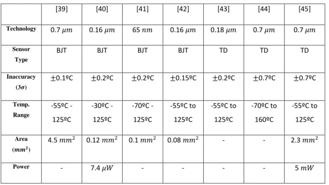
For a better understanding of the major differences involved in the different types of temperature sensors described so far, an informative table (Tab.2.1) is presented next with their most relevant key performance parameters.
Table 2.1: Performance summary and comparison with other state-of-the-art sensors reported in the literature. [39] [40] [41] [42] [43] [44] [45] Technology 0.7 𝜇𝑚 0.16 𝜇𝑚 65 𝑛𝑚 0.16 𝜇𝑚 0.18 𝜇𝑚 0.7 𝜇𝑚 0.7 𝜇𝑚 Sensor Type BJT BJT BJT BJT TD TD TD Inaccuracy (3𝝈) ±0.1ºC ±0.2ºC ±0.2ºC ±0.15ºC ±0.2ºC ±0.7ºC ±0.7ºC Temp. Range -55ºC - 125ºC -30ºC - 125ºC -70ºC - 125ºC -55ºC to 125ºC -55ºC to 125ºC -70ºC to 160ºC -55ºC to 125ºC Area (𝒎𝒎𝟐) 4.5 𝑚𝑚2 0.12 𝑚𝑚2 0.1 𝑚𝑚2 0.08 𝑚𝑚2 - - 2.3 𝑚𝑚2 Power - 7.4 𝜇𝑊 - - - - 5 𝑚𝑊
11
Chapter
3
In the present chapter, the design of a thermal-diffusivity temperature sensor with an embedded CCO-based phase domain ΔΣ modulator will be presented. All main components of this sensor will be described, and included, later on, in the composition of the final block diagram of the complete sensor system.
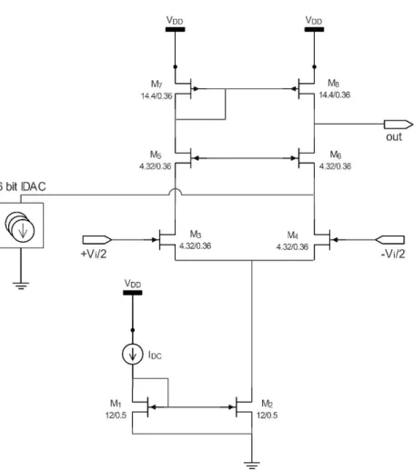
The circuit of this thermal-diffusivity temperature sensor is composed by a digital part (comprising D and JK flip-flops, a 6 bit counter, and several NMOS, PMOS and CMOS switches), and by an analog part (comprising a current-controlled oscillator (CCO), a transconductance stage (gm), a 6 bit current-mode DAC (IDAC) and an electro-thermal filter (ETF)), as can be seen in Fig.3.1.
Figure 3.1 – Block diagram of the proposed thermal diffusivity temperature sensor with a CCO-based phase-domain ΔΣ modulator, and the corresponding timing diagram [48].
Design of the Main
Building-Blocks
12
3.1. Flip-Flops
Flip-flops and latches are used as data storage elements. They are the basic memory elements used in clocked sequential circuits. Such circuits are binary cells with capacity to store one bit of information. It has two outputs, first for the normal value and the second for the complement value of the bit stored in it. There are many ways where binary information can enter a flip-flop. A flip-flop has an important characteristic, the output can exist in one of the two stable states, logic 1 and logic 0, simultaneously, which is supported by the appropriate crossed feedback connections associated with the most common form of flip-flop called as a latch.
Flip-flops and latches are a fundamental building block of digital electronics systems used in computers, communications, and many other types of systems. Computers use huge amounts of flip-flops, creating a need to coordinate their working, through a square wave signal known as clock signal (CLK) that is applied to the flip-flop, preventing the flip-flop from changing state until the right instant occurs [34].
There are many types of flip-flops, as D, JK, RS and T flip-flops, that are also called “latches”, “bistable multivibrators”, or “binaries”. Functional flip-flops can be made from logic gates, or be available in IC form. They are connected to form sequential logic circuits for data storage, counting, timing and sequencing [19].
The major difference between a latch and a flip-flop, is that a latch is a sequential circuit that changes their outputs depending on inputs, without any intervention of clock. While a flip-flop is a sequential circuit more controllable, that changes their outputs only by the action of clock [21]. One of flip-flop’s characteristics is that if a flip-flop circuit is always provided with power, it can maintain a binary state indefinitely until directed by an input signal to switch states. The number of inputs and the manner, in which the inputs affect the binary state, are the biggest differences among various types of flip-flops [18][20].
3.1.1. D Flip-Flop
The logic symbol for a common type of flip-flop is shown in Fig. 3.2. The D flip-flop has only a single data input (D) and a clock input (CLK). The customary Q and Q’ outputs are shown on the right side of the symbol. The D flip-flop is often called a delay flip-flop. This name accurately describes the unit’s operation. Whatever the input at the data (D) point, it is delayed from getting to the normal output (Q) by one clock pulse. Data is transferred to the output on the transition of the clock pulse [19].
13
The D flip-flop receives the designation from its ability to hold data into its internal storage. The binary information present at the data input of the D flip-flop is transferred to the Q output when the Clk input is enabled. The output follows the data input as long as the pulse remains in its 1 state. When the pulse goes to 0, the binary information that was present at the data input at the time the pulse transition occurred is retained at the Q output until the pulse input is enabled again [18].
Figure 3.2 – Logic symbol for edge-triggered negative D flip-flop.
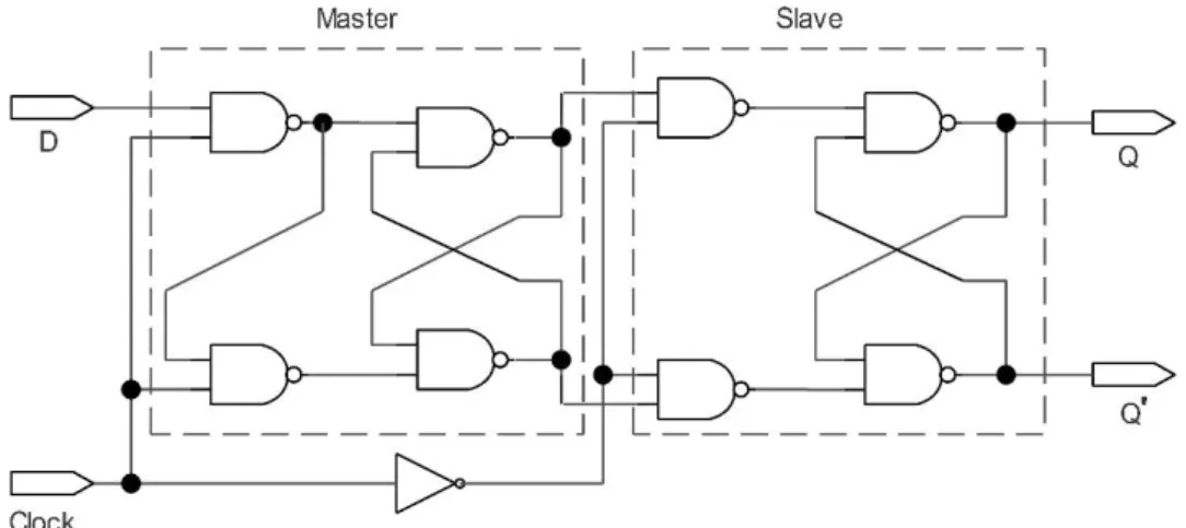
The edge-triggered D flip-flop is a modification of its RS counterpart [20]. It can be achieved
replacing the R input with an inverted version of the S input, which thereby becomes D. This procedure is only done in the master latch section, leaving the slave unchanged, as presented in Fig. 3.3.
Figure 3.3 – Circuit schematic of a master-slave negative edge-triggered D flip-flop.
A master-slave D flip-flop is created by connecting two gated D latches in series, and inverting the enable input to one of them. It is called master–slave because the second latch in the series only changes in response to a change in the first (master) latch.
Observing the logic symbol for D flip-flop in Fig. 3.2, the clock (CLK) input has a small > inside the symbol, meaning that this is an edge-triggered device, and the presence of a bubble at the triangle means that this D flip-flop is triggered on the negative going edge [21].
14
This ngative edge-triggered flip-flop transfers data from input D to output Q on the HIGH-to LOW transition of the clock pulse, in other words, it is the change of the clock from HIGH to LOW (or H to L) that transfers data [19], as confirmed through the observation of the Tab. 3.1.
Table 3.1 – Truth table of a master-slave negative edge-triggered D flip-flop.
Inputs Outputs Comments D CLK Q Q´ 1 ↓ 1 0 Set 0 ↓ 0 1 Reset X 0 Q0 Q’0 X 1 Q0 Q’0
In negative edge-triggered flip-flop the Master is running with CLK and Slave with CLK’, instead of positive edge-triggered flip-flop, where the Slave is controlled by CLK and Master by CLK’, as can be seen in Fig 3.4 and Fig. 3.5.
Figure 3.4 – Representation of a master-slave negative edge-triggered D flip-flop.
15
3.1.2. JK Flip-Flop
A JK flip-flop have similarities with RS flip-flop with the indeterminate state of the last one
flip-flop being defined in the first one flip-flop, with the inputs J and K working like inputs S and R to set and clear the flip-flop. Set is controlled by input J and reset is controlled by input K, and when both inputs J and K are activated, the flip-flop changes to its complement state [18][20].
The JK flip-flop used in this project is a negative master-slave flip-flop with set and clear,
constituted by two 2 input NAND gates, six 3 input NAND gates and one inverter, as can be seen in Fig. 3.6.
Figure 3.6 – Circuit schematic of master-slave negative JK Flip-Flop with set and clear.
3.2. The Digital Counter
Counters are important digital electronic circuits, and are used extensively in the design of digital systems and are classified as standard items [20]. They are sequential logic circuits because timing is important and they need a memory characteristic. Digital counters have some important characteristics as maximum number of counts (modulus of counter), up or down count, asynchronous or synchronous operation, and are free-running or self-stopping. As with other sequential circuits, flip-flops are used to construct counters [19].
A counter is essentially a register/sequential circuit that goes through a predetermined
16
in such a way as to produce a prescribed sequence of binary states in the register. Counters are extremely useful in digital systems, and can be used to count events such as a number of clock pulses in a given time (measuring frequency). They can be used to divide frequency and store data as in a digital clock, and they can also be used in sequential addressing, in some arithmetic circuits, and for generating timing variables to sequence and control the operations in a digital system [18][19].
3.2.1. Synchronous 6-bit Up/Down Binary Counter
In a synchronous counter, all flip-flops are triggered simultaneously by the counting clock pulse. As shown in the counter of this work, all Clk terminals are connected to the count pulse [20].
In a synchronous count-down binary counter, the flip-flop in the lowest-order position is complemented with every pulse. A flip-flop in any other position is complemented with a pulse provided all the low-order bits are equal to 0. For example, if the present state of a 6-bit count-down binary counter is 𝑄6𝑄5𝑄4𝑄3𝑄2𝑄1 = 110000, the next count will be 101111. 𝑄1 is always
complemented. 𝑄2 is complemented because the present state of 𝑄1 = 0. 𝑄3 is complemented
because the present state of 𝑄2𝑄1 = 00. 𝑄4 is complemented because the present state of 𝑄3𝑄2𝑄1
= 000. 𝑄5 is complemented because the present state of 𝑄4𝑄3𝑄2𝑄1 = 0000. But 𝑄6 is not
complemented because the present state of 𝑄5𝑄4𝑄3𝑄2𝑄1 = 10000, which is not an all-0’s
condition [18].
The counter used in this work/project is a synchronous 6-bit up/down binary counter presented in Fig. 3.7. Basing on analysis obtained through the simulation, when the up/down input control is 1, the circuit counts up, since the J and K inputs receive their signals from the values of the previous normal outputs of the flip-flops. When the up/down input control is 0, the circuit counts down, since the complemented outputs of the previous flip-flops are applied to the J and K inputs [18].
17
Figure 3.7 – Circuit schematic of synchronous 6 bit up/down binary counter.
3.3. Controlled Oscillators
Oscillators are an integral part of many electronic systems. In their design and construction different topologies and performance parameters are required, because of many applications that the same can have. Oscillators are normally embedded in a phase-locked system (PLL), and some of the challenges in their CMOS design are robustness and high-performance [29][30].
An electrical oscillator generates a periodically time-varying output signal (sinusoidal sine wave or square wave, saw-tooth or triangular shaped waveforms, or just a train of pulses of a variable or constant width) from DC power. As such, the circuit must involve a self-sustaining mechanism that allows its own noise to grow and eventually become a periodic signal [22]. An oscillator is basically an amplifier with positive feedback, or regenerative feedback (in-phase). There are many types of oscillators, various forms of oscillator implementations, and many different circuit configurations that produce oscillations; tuned-circuit oscillators (LC tuned oscillators, FET oscillators, BJT oscillators, op-amp oscillators, delay-line oscillators, voltage controlled oscillators), crystal oscillators (PI-network oscillators, ceramic-resonator oscillators, SAW oscillators), negative-resistance oscillators (dielectric-resonator oscillators, YIG oscillators), and non-sinusoidal oscillators (relaxation oscillators, ring oscillators, triangular-wave oscillators, saw-tooth oscillators, oscillators using 555 timer). Some oscillators produce sinusoidal signals, others produce non-sinusoidal signals. Sinusoidal oscillators are used in many applications, as in wireless systems, in consumer electronic equipment, and in test equipment. Non-sinusoidal oscillators, such as pulse and ramp/saw-tooth oscillators are used in timing and control applications. Pulse oscillators are normally found in digital-systems clocks, and ramp oscillators are found in the horizontal sweep circuit of oscilloscopes and television sets [23][27].
18
The feedback, that is one of the most important electrical engineering concepts, is approached in oscillator design. The feedback consists in add or subtract to the input variable of a system a quantity proportional to output variable [28].
The basic components in a feedback oscillator are the amplifier, an amplitude-limiting component, a frequency-determining network, and a (positive) feedback network. Normally the amplifier likewise acts as the amplitude-limiting component. The frequency-determining network often performs the feedback function. The feedback circuit is essential to return some of the output signal back to the input. Moreover, the positive feedback takes place when the feedback signal is in phase with the input signal. Once verified the necessary conditions, is possible to have oscillation [23]. In other words, an oscillator is an amplifier, which uses positive feedback that generates an output frequency without the use of an input signal. It is self-sustaining.
At start-up, however, oscillation is triggered by transients or noise, after which a properly designed oscillator will reach a stable oscillation state [25].
The presence of a loop at the core of any oscillator circuit causes a positive feedback at a selected frequency [26]. Fig. 3.8, provides the generic closed-loop system representation.
Figure 3.8 – Closed-loop circuit model of basic feedback oscillator configuration.
From Fig. 3.8 we can write
𝑉𝑜𝑢𝑡 = 𝐻𝐴(𝑗𝜔) ∙ 𝑉𝑑
(3.1)
𝑉𝑓= 𝐻𝐹(𝑗𝜔) ∙ 𝑉𝑜𝑢𝑡
(3.2)
and
𝑉𝑑= 𝑉𝑖𝑛+ 𝑉𝑓
(3.3)
By combining the transfer functions of the amplification stage 𝐻𝐴(𝜔) with the feedback stage
𝐻𝐹(𝜔) to the closed-loop transfer function, can be established the mathematical condition for a
19
𝑉𝑜𝑢𝑡
𝑉𝑖𝑛
= 𝐻
𝐶𝐿(𝑗𝜔) =
𝐻𝐴(𝑗𝜔)
1−𝐻𝐹(𝑗𝜔)𝐻𝐴(𝑗𝜔) (3.4)
Since there is no input to an oscillator, 𝑉𝑖𝑛 = 0, to obtain a nonzero output voltage, 𝑉𝑜𝑢𝑡, the
denominator in (3.4) has to be zero. This requirement leads to the Barkhausen criterion, which is also known as the loop gain equation:
1 − 𝐻𝐹(𝑗𝜔)𝐻𝐴(𝑗𝜔) = 0 (3.5)
or
𝐻𝐹(𝑗𝜔)𝐻𝐴(𝑗𝜔) = 1 (3.6)
Equation (3.6) expresses the fact that for oscillations to occur the loop gain must be unity, satisfying the Barkhausen criterion.
With 𝐻𝐴(𝑗𝜔) = 𝐻𝐴𝑜 and
𝐻𝐹(𝑗𝜔) = 𝐻𝐹𝑟(𝜔) + 𝑗𝐻𝐹𝑖(𝜔) (3.7)
where 𝐻𝐹𝑟(𝜔) and 𝐻𝐹𝑖(𝜔) are the real and imaginary parts of 𝐻𝐹(𝑗𝜔), we can express (3.6) in the form
𝐻𝐹𝑟(𝜔)𝐻𝐴𝑜+ 𝑗𝐻𝐹𝑖(𝜔)𝐻𝐴𝑜 = 1 (3.8)
Equating the real and imaginary parts on both sides of the equation is obtained
𝐻𝐹𝑟
(𝜔)𝐻
𝐴𝑜= 1 ⇒ 𝐻
𝐴𝑜=
1𝐻𝐹𝑟(𝜔) (3.9)
and
𝐻𝐹𝑖(𝜔)𝐻𝐴𝑜 = 0
⇒
𝐻𝐹𝑖(𝜔) = 0 (3.10)for 𝐻𝐴𝑜≠ 0. The conditions in (3.9) and (3.10) are known as the Barkhausen criteria in
rectangular form for 𝐻𝐴(𝑗𝜔) = 𝐻𝐴𝑜.
The condition (3.9) is known as the gain condition, and (3.10) as the frequency of oscillation condition. The frequency of oscillation condition predicts the frequency at which the phase shift around the closed loop is 0° or a multiple of 360°.
The equation (3.6) can also be expressed in polar form as
20 Accordingly, results
|𝐻𝐹(𝑗𝜔)𝐻𝐴(𝑗𝜔)| = 1 (3.11)
and
∠𝐻𝐹(𝑗𝜔)𝐻𝐴(𝑗𝜔) = ±𝑛360° (3.12)
where n = 0, 1, 2, 3, … In equation (3.12) is established the fact that the signal must travel through the closed loop with a phase shift of 0° or a multiple of 360°. For 𝐻𝐴(𝑗𝜔) = 𝐻𝐴𝑜, then
∠𝐻𝐹(𝑗𝜔)𝐻𝐴𝑜 is the angle of 𝐻𝐹(𝑗𝜔), and the equation (3.12) is equivalent to saying that
𝐻𝐹𝑖(𝑗𝜔) = 0, according to (3.10). As well, for 𝐻𝐴(𝑗𝜔) = 𝐻𝐴𝑜 and with 𝐻𝐹𝑖(𝑗𝜔) = 0, equation
(3.11) is reduced to (3.9). The terms in (3.11) and (3.12) are the Barkhausen criteria in polar form [23].
In this work were considered two types of current-controlled oscillators to implement in order to realize the project. The oscillator 1 and oscillator 2, with the differences between both to be described below.
3.3.1. Oscillator 1 (CCO 1)
The oscillator presented here is a ring oscillator composed by an odd number of inverters, in this case three inverters, shown in Fig. 3.9. This configuration of oscillator is best analysed in terms of the time/propagation delay that the signal experiences as it goes through the ring inverters. Considering 𝑡𝑝 the propagation delay of the inverter, the frequency of oscillation is
given by
𝑓
𝑜=
1 2𝑛𝑡𝑝(3.13)
where n is the number of gates.
The data provided by manufacturers of inverters in relation to the propagation delay is as a function or the device load capacitance. Although, the resultant frequency of oscillation can vary substantially from the expected frequency resultant in (3.13).
It is difficult to properly control the frequency of oscillation, since it is controlled by the propagation delay. The propagation delay is affected by many factors, including the variation in
21
output capacitance from unit to unit. The solution for better control of the frequency of oscillation involves adding external elements [23].
Despite high signal distortion and noise, ring oscillators are used in many high speed digital circuits due to an ease of integration, small chip area, high oscillation frequencies and wide tuning ranges [24].
Figure 3.9 – Circuit schematic of oscillator 1 (CCO 1) based on a ring-oscillator configuration.
3.3.2. Oscillator 2 (CCO 2)
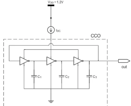
The oscillator covered in this section is the current-starved voltage controlled ring oscillator, and is similar to the oscillator 1, but is composed by more transistors.
CMOS voltage/current controlled oscillator (VCO/CCO) are critical building blocks in phased-locked loops (PLLs), and they are mainly responsible for having the highest fraction of the overall power consumption and occupied area of the system. Furthermore, a VCO/CCO constitutes one of the most important components in many RF transceivers and are commonly associated with signal processing tasks like frequency (channel) selection and signal generation.
VCOs/CCOs occupy an important role in communication systems, giving periodic signals required for timing in digital circuits and frequency translation in RF circuits. The output frequency of a VCO/CCO is a function of a control input, normally a voltage. In an ideal voltage controlled oscillator the output frequency is a linear function of its control voltage.
A current starved VCO/CCO operates similarly to the ring oscillator. The transistors 𝑀4, 𝑀5,
𝑀8, 𝑀9, 𝑀12 and 𝑀13 operate as inverters, while transistors 𝑀3, 𝑀6, 𝑀7, 𝑀10, 𝑀11 and 𝑀14
22
current available to the inverter transistors. In other words, the inverter is starved for current. The drain currents of MOSFETs 𝑀1 and 𝑀2 are the same and are set by the input control voltage. The
currents in transistors 𝑀1 and 𝑀2 are mirrored in each inverter/current source stage [46][47].
Figure 3.10 – Circuit schematic of oscillator 2 (CCO 2).
This oscillator has three stages, and the centre drain current is given as:
𝐼𝐷𝐶𝑒𝑛𝑡𝑟𝑒 = 𝑁 × 𝑉𝐷𝐷× 𝐶𝑡𝑜𝑡× 𝐹𝑐𝑒𝑛 (3.14)
where N is the number of stages of the inverter. The sizes of transistors 𝑀1 and 𝑀2 are
deter-mined as: 𝐼𝐷𝐶𝑒𝑛𝑡𝑟𝑒
=
𝛽(𝑉𝑔𝑠−𝑉𝑡ℎ𝑛) 2 2 (3.15) where, 𝛽 =𝐾𝑝∙𝑊 𝐿 .The oscillation frequency of the current-starved VCO/CCO for N stages is:
𝐹
𝑜𝑠𝑐=
1𝑁
∙ 𝑇
𝐷=
𝐼𝐷23
𝑇𝐷 is the time delay above equation gives the centre frequency of the VCO/CCO when 𝐼𝐷=
𝐼𝐷𝐶𝑒𝑛𝑡𝑟𝑒. Neglecting sub threshold currents, the oscillation of the VCO/CCO is interrupted when
𝑉𝑖𝑛𝑉𝐶𝑂 < 𝑉𝑡ℎ𝑛. Therefore, 𝑉𝑚𝑖𝑛 = 𝑉𝑡ℎ𝑛 and 𝐹𝑚𝑖𝑛 = 0. The maximum VCO/CCO oscillation frequency 𝐹𝑚𝑎𝑥 is determined detecting 𝐼𝐷 when 𝑉𝑖𝑛𝑉𝐶𝑂= 𝑉𝐷𝐷. Thus, at the maximum frequency
𝑉𝑚𝑎𝑥= 𝑉𝐷𝐷 [46][47].
The total capacitance on the drains of transistors 𝑀4 and 𝑀5 for example, is:
𝐶𝑡𝑜𝑡= 𝐶𝑜𝑢𝑡+ 𝐶𝑖𝑛 = 𝐶′𝑜𝑥(𝑊4𝐿4+ 𝑊5𝐿5) + 3 2𝐶 ′ 𝑜𝑥(𝑊4𝐿4+ 𝑊5𝐿5) = =52𝐶′𝑜𝑥(𝑊4𝐿4+ 𝑊5𝐿5) (3.17)
where 𝐶𝑜𝑢𝑡 and 𝐶𝑖𝑛 are the output and input capacitances respectively.
To charge 𝐶𝑡𝑜𝑡 form zero to 𝑉𝑆𝑃 with the constant current 𝐼𝐷3 is taken a certain amount of time
that is expressed by:
𝑡
1= 𝐶
𝑡𝑜𝑡∙
𝑉𝑆𝑃𝐼𝐷3 (3.18)
where 𝑉𝑆𝑃 is switching point of the inverter.
And the time 𝐶𝑡𝑜𝑡 takes to discharge from 𝑉𝐷𝐷 to 𝑉𝑆𝑃 is expressed by:
𝑡
2= 𝐶
𝑡𝑜𝑡∙
𝑉𝐷𝐷−𝑉𝑆𝑃𝐼𝐷6 (3.19)
Setting 𝐼𝐷3= 𝐼𝐷6= 𝐼𝐷 (which will be designated by 𝐼𝐷𝑐𝑒𝑛𝑡𝑟𝑒 when 𝑉𝑖𝑛𝑉𝐶𝑂=
𝑉𝐷𝐷
2 ), then the sum
of 𝑡1 and 𝑡2 will be:
𝑡
1+ 𝑡
2=
𝐶𝑡𝑜𝑡∙𝑉𝐷𝐷
𝐼𝐷 (3.20)
3.4. Transconductance Stage (gm)
The transconductance stage (gm) is mainly built using a differential-pair with active loads. A differential pair is a basic circuit in electronics. It can be used as an amplifier with differential
24
input, constituting the input stage of the operational amplifiers, which determines most of the non-ideal characteristics of these amplifiers. In some cases, a differential pair with active loads behaves itself as a moderate gain operational transconductance amplifier (OTA).
Differential pairs and differential transconductors, in general can be used in analog continuos-time filters (Gm-C filters), RC-active filters analog multipliers and in many other circuits derived from it, such as modulators and phase detectors. The differential pair with active loads is the fundamental constituent of analog and mixed-signal integrated circuits [35].
3.5. Digital-to-Analog Converter
The conversion between analog and digital signals is one of the most important functions in signal processing. There are areas where signal processing is done on analog signals and areas where the signal processing is done on digital signals. Hence, there is a need to convert analog-to-digital and digital-to-analog between the two types of signals. Thus, these converters, respectively ADCs and DACs, play an important role in any signal-processing system [33]. The different approaches to convert a digital signal to an analog signal include speed, chip area, power efficiency and achievable accuracy. Wherein, for a given and specific application, it is necessary to know which converter algorithms or architectures to choose.
DACs are sampled data systems, thus they require the use of circuit techniques that can deal with discrete-time analog signals. The circuits are frequently divided into voltage-mode or current-mode circuits, according the analog signals are voltages or currents. In CMOS, for voltage-mode circuits is normally used the switched-capacitor (SC) technique while for current-mode circuits is used the switched-current (SI) technique [31].
The DAC input is a digital information made of parallel binary signals generated from a digital signal-processing system. These parallel binary signals go through conversion process to a similar analog signal. In the output, the analog signal can be amplified and/or filtered before being applied to an analog signal-processing system. The input and output in most DAC’s are voltage signals, although, they can be other physical quantities, such as current or charge [32][33].
In other words, DAC is a digital-to-analog converter, that has a function to convert digital data
into an analog signal, that can be a current, a voltage or simply an electric charge. That device is responsible for converting an abstract finite-precision number into a physical quantity/concrete sequence of impulses, which is subsequently processed by a reconstruction filter.
There are many different DAC architectures, that include Nyquist-Rate DAC, Binary Weighted DAC (Current-Steering DAC, R-2R Ladder DAC, Charge Redistribution DAC), Thermometer Coded DAC, Encoded DAC, Hybrid DAC, Low-Speed DAC (Algorithmic DAC,
25
Switched-Current Algorithmic DAC), Pipelined DAC, Oversampling DAC (M-bit DAC), and Delta-Sigma DAC.
The block diagram presented in Fig. 3.11, describes a DAC with voltage output. It consists of a reference voltage 𝑉𝑅𝐸𝐹, and digital information of N-bits (𝑏0, 𝑏1, … , 𝑏𝑁−1) where 𝑏0 is the most
significant bit (MSB), and 𝑏𝑁−1 is the least significant bit (LSB). The voltage output 𝑉𝑜𝑢𝑡 can be
mentioned as
𝑉𝑜𝑢𝑡= 𝐾𝑉𝑅𝐸𝐹𝐷 (3.21)
where K is a scaling factor and the digital information D is given as
𝐷 =
𝑏0 21+
𝑏1 22+ ⋯ +
𝑏𝑁−1 2𝑁 (3.22)where N is the total number of bits of the digital word and 𝑏𝑖−1 is the ith-bit coefficient and is 0
or 1. Thence, the output of a DAC can be expressed matching eq. (3.21) and (3.22) to obtain
𝑉𝑜𝑢𝑡= 𝐾𝑉𝑅𝐸𝐹 = [ 𝑏0 21
+
𝑏1 22+ ⋯ +
𝑏𝑁−1 2𝑁 ](3.23) or 𝑉𝑜𝑢𝑡 = 𝐾𝑉𝑅𝐸𝐹 = [𝑏02−1+ 𝑏12−2+ ⋯ + 𝑏𝑁−12−𝑁] (3.24)
Figure 3.11 – Digital-analog converter (DAC) in applications of signal-processing.
In order to understand the design of DAC, it is important his characterization. There are two important performance characteristics of digital-analog converters, namely static and dynamic properties. The DAC’s resolution is given by the number of bits in the applied digital input information. Its resolution is expressed as N-bits, where N is the number of bits. In Fig. 3.12, is
26
presented the output characteristic of an ideal 3-bit DAC (N = 3). For each of eight possible digital words matches its own unique analog output voltage, whose levels are separated by an LSB, and ist value can be expressed as
𝐿𝑆𝐵 =
𝑉𝑅𝐸𝐹2𝑁 (3.25)
and as the digital word increases by 1-bit, the output of the ideal DAC must jump by 1 LSB [33].
Figure 3.12 – Ideal characteristics of input-output for 3-bit DAC.
As the resolution of the DAC is not infinite, the maximum analog output voltage is different from 𝑉𝑅𝐸𝐹. The full-scale (FS) value of the DAC describes this result. The difference between the
analog output for the largest digital word (111) and the analog output for the smallest digital word (000) defines the full-scale value. Usually, the DAC’s full scale can be established as
Full Scale (FS) = 𝑉𝑅𝐸𝐹− 𝐿𝑆𝐵 = 𝑉𝑅𝐸𝐹 (1 − 1
2𝑁) (3.26)
and the full-scale range (FSR) is defined as
𝐹𝑆𝑅 = lim
𝑁→∞𝐹𝑆 = 𝑉𝑅𝐸𝐹 (3.27)
27
An important aspect about DAC relates to certain types of errors. There should be a unique analog output signal for each digital word, and any gap from ideal n-bits resolution characteristic belongs to static-conversion errors. These type of errors include, gain errors, offset errors, differential nonlinearity, integral nonlinearity, and monotonicity. Wherein gain error is the difference between the actual finite resolution and an infinite resolution characteristic measured at the rightmost vertical jump. Offset error is a constant difference between the actual finite resolution characteristic and the ideal finite resolution characteristic measured at any vertical jump. Differential nonlinearity ia a measure of the separation between adjacent levels measured at each vertical jump. Integral nonlinearity is the maximum difference between the actual finite resolution characteristic and the ideal finite resolution characteristic measured vertically. And monotonicity means that as the digital input to the converter increases over its full-scale range, the analog output never exhibits a decrease between one conversion step and the next [33].
3.5.1. The 6 bit IDAC
The DAC presented in this work is a 6 bit IDAC shown in Fig. 3.13
The architecture of this IDAC is based on a current-steering approach and it consists of a current replication network which generates weighted currents in the form of independent current sources, a current switching network controlled by the binary bits, and a resistance 𝑅1 responsible
for converting the current to voltage.
In other words, this IDAC comprises six input inverters, each one connected to its unit device circuit. The number of unit device circuits corresponds to the number of bits of this DAC, wherein each unit device circuit has a certain width value in all its transistors. Starting from the lower unit device circuit (the least significant weight) to the upper unit device circuit (the most significant weight), the width value grows exponentially with a power of 2 between each unit device circuit. The DAC number-of-bits presented in this work is determined by the resolution (N) of bits, with N = 6, and satisfying the equation 2𝑁 = nº of levels, results in 26= 64 levels (LSBs). This 6 bit IDAC for a certain digital input code corresponds to a given analog output voltage.
28
Figure 3.13 – Simplifier circuit schematic of 6 bit IDAC.
Each of the unit device circuit has an NMOS cascode current-source, whose transistors are
sized up according to the corresponding bit weight and are biased by the same bias voltages. This type of current source was preferred in detriment to the simple current source, because, cascode current source presents a higher output impedance that makes the IDAC more accurate. Requires
29
switches, mainly built by NMOS and PMOS devices, have their sizes are scaled up according to the bit values as well. In this case, partitioning is applied to the weighted sources and each weighted current source is made of a number of LSB devices connected in parallel, where the LSB device becomes the unit device. By partitioning the weighted devices in units so that the MSB consists of 2𝑁−1 unit devices, as can be seen in a theortical example presented in Fig.3.14 [38].
Figure 3.14 – Simple-binary weighted current steering DAC and its implementation with transistors [38].
This type of implementation is compact and very simple, presenting high rates of conversion, but is limited by the process limitations, by the maximum switching speed switching the current, and by the steepness of the of the data waveforms carrying the bits. Also, there are some disadvantages of this type of circuit realization that results in a limitation of its performance, mainly because of its simplicity and low power consumption.
One of these problems is associated with the weighted impact of switching problems, also named MSB/LSB glitches. This condition is verified because of imperfect synchronization of the data waveforms that control the current switches. As an example, in a 8 bit binary weighted DAC at the midscale transition 01111111 → 10000000 the MSB current source turns on and all the remaining bits turn off. Also, if the MSB source turns on a bit earlier than the remaining sources turn off, then for a time interval the code 11111111 will appear before the 10000000. And this momentary voltage spike, that is the principal carry glitch in the normal operation of the DAC, is responsible for creating a harmonic distortion.
As a solution for these types of glitches of CS DAC’s, have been created and implemented the famous de-glitching circuits [38]. However, in the particular case of this work, since the operating speed is not an issue and since the required resolution is quite low (N = 6 bits), none of the previously referred problems represent a critical problem for the temperature sensor system.
![Figure 1.1 – Block diagram of the proposed thermal diffusivity temperature sensor with a CCO-based phase-domain ΔΣ modulator, and the corresponding timing diagram [48]](https://thumb-eu.123doks.com/thumbv2/123dok_br/19227794.965792/20.892.205.702.108.481/figure-diagram-proposed-thermal-diffusivity-temperature-modulator-corresponding.webp)


![Figure 3.18 – Simplified schematic layout (a), and photomicrograph (b) of the optimized CMOS ETF [50]](https://thumb-eu.123doks.com/thumbv2/123dok_br/19227794.965792/51.892.191.700.115.297/figure-simplified-schematic-layout-photomicrograph-optimized-cmos-etf.webp)