Mestrado em Engenharia Eletrotécnica
LLC Resonant Charger with Variable Inductor
Control
Trabalho de Projeto apresentado para a obtenção do grau de Mestre em
Engenharia Eletrotécnica – Área de Especialização em Automação e
Comunicações em Sistemas Industriais
Autor
Válter de Sousa Costa
Orientador
Professora Doutora Marina Mendes Sargento Domingues
Perdigão
Departamento de Engenharia Eletrotécnica – Instituto Superior de Engenharia de Coimbra – Instituto Politécnico de Coimbra (DEE-ISEC-IPC); Instituto de Telecomunicações – Coimbra (IT-Coimbra)
Co-Orientador
Professor Doutor André Manuel dos Santos Mendes
Departamento de Engenharia Eletrotécnica e de Computadores – Universidade de Coimbra (DEEC-FCTUC); Instituto de Telecomunicações – Coimbra (IT-Coimbra)
ACKNOWLEDGMENTS
ACKNOWLEDGMENTS
With the conclusion of this work I would like to thank, firstly to Professor Marina Perdigão (Departamento de Engenharia Eletrotécnica – Instituto Superior de Engenharia de Coimbra – Instituto Politécnico de Coimbra, DEE-ISEC-IPC and Instituto de Telecomunicações – Coimbra, IT-Coimbra) and Professor André Mendes (IT-Coimbra and, Departamento de Engenharia Eletrotécnica e de Computadores – Universidade de Coimbra, DEEC-UC) for guiding me and helping me in order to complete this work.
To ISEC-IPC that received me and, where I took by bachelor degree in Electrotechnical Engineering and where I am now taking the master degree in Electrotechnical Engineering.
To IT-Coimbra for receiving me, allowing me to complete this work in the Laboratório de Sistemas Energéticos, and for the financial support that allowed building the experimental prototype.
To all of the professors in general that in the last few years have been helping me improve myself and gain knowledge in this field.
To all my colleagues from the Laboratório de Sistemas Energéticos, for their help and cooperation.
To all my family and friends for the cooperation, comprehension and moral support in the most trouble days.
ABSTRACT
ABSTRACT
The present work pretends to study the operation and behavior of the LLC resonant converter topology considering a battery charging application, using the traditional switching frequency control and a new control variable, the variable inductance, provided by a current controlled device, the Variable Inductor (VI).
During this work, a brief state of the art regarding general types of power converters and resonant power converters is presented. The LLC resonant converter topology and its advantages and disadvantages are described. The VI principle of operation and structure is presented and discussed and, in the end some information about batteries and its behavior under charging and discharging conditions is presented. The considered batteries characteristics for the studied battery charger are shown and the adopted charging profile is presented.
In the following chapters, a theoretical analysis of the LLC resonant converter operation and behavior under switching frequency or VI control is performed and presented. A design methodology is proposed for the converter considering both switching frequency and VI control, separately or simultaneously. Simulations of the converter operation under open-loop condition were made, and simulation results were obtained and discussed.
A prototype was built and test results were obtained. The prototype uses a SiC MOSFET (Silicon Carbide Metal Oxide-Semiconductor Field Effect Transistor) based inverter working at 100 kHz controlled with fiber optic drivers. To build the prototype, Printed Circuit Boards (PCB) were designed, manufactured and built. An high-frequency transformer and a VI were also design and built. Finally, theoretical, simulation and experimental results are confronted in order to reach conclusions regarding to the proposed design methodology and the prototype operation. This final analysis allows validating the LLC-VI resonant converter as a good option for a battery charger.
Keywords: LLC Resonant Converter; Variable Inductor; DC-DC Power Converters;
RESUMO
RESUMO
O presente trabalho apresenta um estudo sobre o comportamento e operação do conversor ressonante LLC considerando uma aplicação de carregamento de baterias. Esta análise considera o tradicional método de controlo usando a frequência de comutação e, implementando uma nova variável de controlo para este tipo de conversores de potência, a Bobina de Indutância Variável (BIV) – Variable Inductor (VI).
Os conversores de potência baseados em topologias ressonantes têm vantagens relativamente aos tradicionais conversores controlados usando técnicas de PWM (Pulse-Width Modulation). Algumas das vantagens são: a possibilidade de trabalhar a frequências de comutação mais elevadas, reduzindo assim o tamanho dos conversores; operação em modo ZVS (Zero Voltage Switching), reduzindo as perdas por comutação. A topologia utilizada, o conversor ressonante LLC tem vindo a ser estudada nos últimos anos devido a estas vantagens quando comparada a outras topologias ressonantes, como o conversor ressonante série ou o conversor ressonante paralelo.
A Bobina de Indutância Variável é um elemento magnético que permite, de forma controlada, variar o valor da indutância da bobina através da regulação do nível de saturação do núcleo. Este elemento magnético tem tido aplicações variadas no que respeita ao controlo de conversores de eletrónica de potência, nomeadamente em aplicações de energias renováveis, controlo de lâmpadas LED (Light Emitting Diode) e, em particular, em conversores ressonantes.
Neste trabalho é apresentado um breve estado da arte sobre os tipos de conversores de potência assim como os tipos de conversores ressonantes, introduzindo a topologia em estudo, o conversor ressonante LLC, bem como as suas vantagens e desvantagens. O princípio de funcionamento e estrutura da BIV são apresentados. Por fim, informação adicional sobre o funcionamento e comportamento das baterias durante os processos de carga e descarga é apresentada e discutida. São ainda apresentadas as características das baterias consideradas para a aplicação em estudo bem como os perfis de carregamento adoptados.
conversor. Por fim, o impacto da frequência de comutação e da BIV no funcionamento do conversor ressonante LLC é analisado.
A análise teórica efectuada permite compreender o funcionamento e comportamento do conversor ressonante LLC quando controlado através da frequência de comutação ou, utilizando o método de controlo proposto, utilizando uma BIV. Uma metodologia de cálculo é proposta, a qual permite dimensionar o conversor para ser controlado usando a frequência de comutação ou a BIV, separadamente ou em simultâneo. Desta análise resultou um ficheiro em Mathcad que implementa a metodologia de cálculo proposta, permitindo assim projetar o conversor ressonante LLC para uma determinada aplicação. Os principais parâmetros para projetar o conversor ressonante LLC são: o nível de tensão do barramento DC que alimenta o conversor, a frequência de comutação do inversor de meia-ponte e, os valores de tensão e corrente de saída. Através dos resultados teóricos e de gráficos obtidos, é possível analisar o comportamento e operação do conversor em função das variáveis de controlo (frequência de comutação e BIV) e da carga. Durante a análise teórica considera-se que a carga é uma carga resistiva com valor equivalente que permite emular o comportamento, neste caso, da bateria num determinado ponto de operação específico, equivalente a um estado de carga.
Simulações são então conduzidas utilizando o software PSIM (Power Electronics Simulation Software), que permite obter formas de onda e medidas de valores de tensão e de corrente em diversos pontos do circuito, que permitem comprovar o seu funcionamento. Os resultados foram obtidos com controlo em malha aberta.
RESUMO faz parte do circuito ressonante, permitindo o isolamento galvânico entre a entrada e a saída do conversor; e o protótipo de uma BIV, que permite efetuar o controlo do conversor mantendo a frequência de comutação constante. Após montagem do setup experimental, foi possível realizar testes experimentais e obter resultados relativamente à operação e comportamento do conversor ressonante LLC.
Resultados teóricos, de simulação e experimentais são confrontados ao longo do trabalho por forma a comprovar a veracidade do método de cálculo proposto, bem como a operação do protótipo do conversor ressonante LLC controlado usando a BIV. Os resultados teóricos e simulados são muito similares o que prova a veracidade da metodologia de projeto proposta. Os objetivos inicialmente previstos foram atingidos no que diz respeito à validação da topologia proposta, com este parâmetro de controlo alternativo, com a finalidade de aplicação em carregadores de baterias. No entanto, visto que o protótipo ainda se encontra em fase de otimização, os testes foram apenas efetuados a um nível de potência mais baixo quando comparado com o valor nominal. Pretende-se como trabalho de continuação, a implementação do controlo em malha fechada, e do teste com o banco de baterias de acordo com as especificações escolhidas. A eficiência obtida nessas condições deverá melhorar no que diz respeito ao registo obtido na fase experimental.
O trabalho foi desenvolvido no Laboratório de Sistemas Energéticos (LSE) do Instituto de Telecomunicações – Coimbra (IT-Coimbra), onde foi possível realizar a análise teórica e de simulação, bem como, proceder ao projeto e construção do protótipo e do setup experimental necessário para obtenção dos resultados experimentais. As PCBs projetadas foram fabricadas no Gabinete Técnico de Electrotecnia (GTE) do Instituto Superior de Engenharia de Coimbra (ISEC) – Instituto Politécnico de Coimbra (IPC). As PCBs foram então montadas e testadas no LSE.
A realização deste trabalho permitiu algumas contribuições para o grupo de investigação do IT-Coimbra e não teria sido possível sem o apoio de ambas as instituições envolvidas, o ISEC e o IT.
Palavras-Chave: Conversor Ressonante LLC; Bobina de Indutância Variável (BIV);
INDEX
INDEX
ACKNOWLEDGMENTS ... i
ABSTRACT ... iii
RESUMO ... v
INDEX ... ix
LIST OF FIGURES ... xi
LIST OF TABLES ... xv
LIST OF SYMBOLS ... xvii
LIST OF ACRONYMS ... xxi
GLOSSARY ... xxiii
Introduction ... 1
1. Motivation and Main Objectives ... 2
1.1. Outline of this Work ... 5
1.2. State of the Art ... 7
2. Types of Power Converters ... 7
2.1. Types of Resonant Converters ... 9
2.2. Variable Inductor (VI) ... 13
2.3. VI Principle of Operation ... 13
2.3.1. Batteries ... 15
2.4. LLC Resonant Converter for a Battery Charger ... 21
3. Proposed Battery Charger Application ... 21
3.1. Converter Topology ... 24
3.2. Behavior of the LLC Resonant Converter ... 27
3.3. Operating Modes ... 28
3.3.1. LLC Analysis using FHA ... 30
3.4. Design Methodology and Converter Parameters Design ... 33
3.4.1. VI Control Impact on the Design Methodology ... 35
3.4.2. Control Variables Impact on the Design Methodology ... 38
3.5. VI Control Method ... 38
3.5.1. Switching Frequency Control Method ... 40
Simulation Results ... 43
4. Converter Parameters ... 43
4.1. Simulation Results ... 43
4.2. VI Control Method ... 44
4.2.1. Switching Frequency Control Method ... 45
4.2.2. Prototype and Experimental Results ... 49
5. Converter Parameters ... 51
5.1. Prototype Construction ... 52
5.2. Experimental Results ... 54
5.3. VI Impact in the Converter Operation ... 55
5.3.1. Simulation of a Charging Cycle ... 60
5.3.2. Conclusions, Contributions and Future Work ... 65
6. Conclusions ... 65
6.1. Contributions ... 65
6.2. Future Work ... 66
6.3. Published Articles... 66
6.4. References ... 69
Appendix ... 73
A. Theoretical Analysis of the LLC Resonant Converter ... 75
A.1. LLC Resonant Converter Design ... 75
A.2. Analysis of the k Parameter Impact in the Converter Design ... 101
B. Variable Inductor Design ... 105
C. Prototype Construction Details ... 111
C.1. DC Bus generator ... 113
C.2. LLC-VI Resonant Converter ... 113
C.3. Load ... 123
C.4. Controller... 123
LIST OF FIGURES
LIST OF FIGURES
Figure 1.1 – General configuration of the battery charger ... 2
Figure 2.1 – Four basic converter configurations: a) AC-DC converter; b) DC-DC converterwith isolation; c) DC-AC converter; d) AC-AC converter [8] ... 8
Figure 2.2 – Four basic resonant circuit configurations: a) SS topology; b) SP topology; c) PP topology; d) PS topology ... 9
Figure 2.3 – Two basic topologies for resonant converters: a) Half-bridge series resonant converter; b) Half-bridge parallel resonant converter [9] ... 12
Figure 2.4 – VI core: a) ETD shaped core [19]; b) ETD core for VI construction ... 14
Figure 2.5 – Assembly and Magnetic contribution of the different windings in the VI: a) DC windings assembly and magnetic flux contribution; b) Main winding assembly and magnetic contribution; c) Complete VI model with DC and main windings assembled [16] ... 14
Figure 2.6 – Typical discharge characteristics for batteries [22] ... 16
Figure 2.7 – Typical charging characteristics for batteries: a) Lead Acid and Li-Ion batteries; b) Ni-MH and Ni-CD batteries [22] ... 16
Figure 2.8 – Problems during charging: a) Constant voltage charging; b) Constant current charging [23]... 17
Figure 2.9 – Current and voltage of a battery during the charging process [23] ... 18
Figure 2.10 – Battery charger for EV block diagram [25] ... 19
Figure 2.11 – Types of charging systems: a) On-board charger fed by AC power from the grid; b) On-board charger fed by DC power; c) Charger divided between the charging station and the vehicle; d) Battery charger on the charging station ... 20
Figure 3.1 – Battery charger based on the LLC resonant converter block diagram: a) Simple block diagram; b) Block diagram with the block of the LLC resonant converter ... 21
Figure 3.2 – Battery voltage and current profiles and, behavior of and values along the charging process: (a) control and, (b) control [29] ... 23
Figure 3.3 – LLC Resonant Converter – Typical Topology [10] ... 24
Figure 3.4 – LLC Resonant Converter – Simplified Topology [9] ... 25
Figure 3.5 – Typical waveforms of the Half-bridge LLC Resonant Converter [9] ... 26
Figure 3.6 – LLC-VI Resonant Converter – Proposed Topology ... 27
Figure 3.7 – Typical gain curves of LLC resonant converter for various loads and capacitive and inductive region waveforms [26] ... 28
Figure 3.9 – Voltages and currents definitions ... 30
Figure 3.10 – Derivation of equivalent load resistance [27] ... 32
Figure 3.11 – AC equivalent circuit for LLC-VI resonant converter [29] ... 33
Figure 3.12 – Simplified AC equivalent circuit for LLC resonant converter [29] ... 34
Figure 3.13 – Simplified AC equivalent circuit for LLC resonant converter [26] ... 34
Figure 3.14 – AC equivalent circuit for LLC-VI resonant converter [29] ... 35
Figure 3.15 – Gain curves as function of at 10 and 100 : a) at different load levels; b) at full-load [29]... 39
Figure 3.16 – Output power as function of of , for the operating points corresponding to _0, _90 and _100 [29] ... 40
Figure 3.17 – Gain curves as function of for 10 kHz and 100 kHz design: a) at different load levels; b) at full-load [29] ... 41
Figure 3.18 – Output power as function of of , for the operating points corresponding to _0, _90 and _100 [29] ... 42
Figure 3.19 – Gain curves as function of for 100 kHz design for three different values of at full-load (100% load) [29] ... 42
Figure 4.1 – PSIM circuit for obtaining the simulation results ... 44
Figure 4.2 – Waveforms from simulation which represent the three points of operation correspondent to _0, _90 and _100, in red, green and blue, respectively: (a) 1and 2; (b) 2 ; (c) 1; (d) ; (e) ; (f) ; (g) ; (h) [29] ... 45
Figure 4.3 – Waveforms from simulation which represent the three points of operation correspondent to _0, _90 and _100, in red, green and blue, respectively: (a) 1 and 2 for _0; (b) 1 and 2 for _90; (c) 1and 2 for _100; (d) 2 ; (e) 1; (f) ; (g) ; (h) ; (i) [29] ... 46
Figure 5.1 – Block diagram of the built prototype ... 50
Figure 5.2 – LLC-VI resonant converter full assembly: a) Top view (520 x 400 mm); b) Front view ... 53
Figure 5.3 – Full experimental setup for the LLC-VI resonant converter ... 53
Figure 5.4 – Driver signals for 1 and 2. 1_ , 2_ in blue and red respectively (2V/div) and, 1 and 2 in green and orange respectively (5V/div): a) At 5us/div; b) At 100ns/div ... 54
Figure 5.5 – ! curve ... 55
LIST OF FIGURES Figure 5.7 – Simulation results for " and #, left and right, respectively: (a) and (b) 2 and, $ "; (c) and (d) and, ; (e) and (f) %&; (g) and (h) ' and, & ; (i) and (j) ' and, & = ; (k) and (l) ' , and, ! ; (m) and (n) $ ; (o) and (p)
! ... 58
Figure 5.8 – ! measured curved with experimental results ... 59
Figure 5.9 – a) Charging profile SOC expected points; b) ! curve ... 61
Figure 5.10 – Experimental results for the simulated charging cycle: (a), (b), (c) and (d) $ ", 2 and, , 50V/div, 2A/div; (e), (f), (g) and (h) and ,10V/div, 1A/div; With 2.5us/div ... 62
Figure 5.11 – Simulation of a charging cycle with experimental measured results ... 63
Fig. A.1 – )% theoretical values ... 88
Fig. A.2 –Voltages, currents and Output Power as function of the SOC and , for theoretical and simulation at blue and red, respectively: a) $ SOC; b) ! SOC; c) )% and d) ... 89
Fig. A.3 – Peak gain curves as function of the Q parameter: a) ' - for different values; b) ' - for different = 7 ... 100
Fig. A.4 – Gain curves as function of at 10 and 100 at different load values and for 4 values of for design: a) for = 1; b) for = 7, c) for = 30; d) for = 60 ... 101
Fig. A.5 – Resonant frequency curves as function of at 10 and 100 for 4 values of for design: a) and 0 for = 1; b) and 0 for = 7, c) and 0 for = 30; d) and 0 for = 60 ... 102
Fig. C.1 – Block diagram of the built prototype ... 112
Fig. C.2 – Schematic of the DC bus generator [ref] ... 113
Fig. C.3 – Half-bridge inverter schematic ... 114
Fig. C.4 – Half-bridge inverter PCB prototype (100 x 80 mm), Board design; PCB Top and Bottom Layer and PCB full assembly ... 114
Fig. C.5 –Resonant filter schematic ... 116
Fig. C.6 – Resonant filter PCB prototype (100 x 80 mm), Board design; PCB Top and Bottom Layer and PCB full assembly ... 116
Fig. C.7 – VI parts, assembly and tests: a) ETD 44/22/15 ferrite core; b) Coiling machine; c) VI parts; d) VI full assembly; e) Tests of the VI ... 118
Fig. C.8 – ! measured curved ... 119
Fig. C.9 – Transformer PCB schematic ... 120
Fig. C.11 – Full-bridge rectifier board schematic ... 121
Fig. C.12 – High-frequency Full-Bridge rectifier PCB prototype (100 x 80 mm), Board design; PCB Top and Bottom Layer and PCB full assembly ... 122
Fig. C.13 – Converter load: a) Resistive 5.6 Ω load; b) Programmable DC Electronic Load – BK PRECISION 8522 2400W ... 123 Fig. C.14 – Block diagram of the controller ... 123
Fig. C.15 – Fiber optic drivers PCB, Top and Bottom view and, the assembled drivers in the half-bridge inverter PCB ... 124
Fig. C.16 – Fiber optic emitter board schematic ... 125
Fig. C.17 – Fiber Optic Emitter PCB prototype (62x52 mm), Board design; PCB Top and Bottom Layer and PCB full assembly... 125
Fig. C.18 – Fiber optic emitter and SiC MOSFET drivers experimental test prototype: a) Driver testing; b) Half-bridge inverter testing ... 127
Fig. C.19 – DSP board from Texas Instruments (150 x 65 mm) ... 127
Fig. C.20 – Print screen of the computer monitor. CCS workspace (left), Matlab workspace (Top right) and, Matlab/Simulink block program (Bottom right) ... 128
LIST OF TABLES
LIST OF TABLES
Table 3.1 – Design Specifications ... 22
Table 4.1 – Converter parameters for simulation ... 43
Table 4.2 – Theoretical and simulation results ... 47
Table 5.1 – Converter parameters for simulation and experimental prototype ... 52
Table 5.2 – Converter parameters for simulation and experimental prototype ... 60
Table 5.3 – Theoretical vs. Simulation vs. Experimental Results ... 63
Tab. A.1 – Theoretical and simulation results for the output voltage, current and power as function of the SOC and the VI inductance value ... 88
Tab. A.2 – Gain as function of the k parameter ... 101
Tab. A.3 – Resonant frequency as function of the k parameter ... 103
Tab. C.1 – Half-bridge inverter components list ... 115
Tab. C.2 – Resonant filter components list ... 117
Tab. C.3 – ! measured values ... 119
Tab. C.4 – Transformer PCB components list ... 121
Tab. C.5 – Full-bridge rectifier components list ... 122
LIST OF SYMBOLS
LIST OF SYMBOLS
12 Area of the core cross-section [ 3]
% Capacitor [F]
% Battery Capacitance [Ah]
%4 Output Capacitor [F]
%5 Resonant Capacitor [F]
Duty Cycle [%]
Frequency [Hz]
6 Resonant frequency associated to 6 and %5 [Hz]
7 Switching frequency [Hz]
8 Resonant frequency associated to 5 and %5 [Hz]
; ! Current [A]
!:;<; !4=< Battery current [A]
>4 Output capacitor current [A]
? Current at the output of the full-bridge rectifier diodes [A]
!@A DC control current [A]
?BC; ?3D Series rectifier diodes 1/2 and, 2/3 current [A]
EF Input current [A]
GHE Variable inductor current [A]
GI Magnetizing inductance current in the transformer [A]
4=<; !4=< Output current [A]
!4_JK4;< Minimum output current value / Float current [A]
65E Transformer primary-side current [A]
5; 6 Resonant current [A]
LB; L3 Source current from switches 1 and 2 [A]
k parameter – Ratio between I and KM6
N Length [m]
Inductor [H]
KM6 Transformer primary-side leakage inductance [H]
KM7 Transformer secondary-side leakage inductance [H]
I Magnetizing inductance of the transformer [H]
6 Parallel inductor [H]
5 Resonant inductor [H]
HE Variable inductor inductance [H]
M Voltage gain
" Transformer turns ratio
N Number of turns
Power [VA]
4 Output Power [VA]
- Load quality factor
ℜ Magnetic Reluctance
;A Rectifier input equivalent resistance [Ω]
:;<; G; 4 Battery internal resistance [Ω]
K4;@ Load resistance [Ω]
B ; 3 Half-bridge inverter switches 1 and 2
O Period of time [s]
μ8 Magnetic Permeability in the Vacuum [H/m]
μ5 Magnetic Permeability [H/m]
; $ Voltage [V]
$:;<; $4=< Battery Voltage [V]
LIST OF SYMBOLS
>5 Resonant capacitor voltage [V]
?LB; ?L3 Drain-source voltage from switches 1 and 2 [V]
$Q Rectifier diode voltage drop [V]
R7B; R73 Square wave generator to gate-source from switches 1 and 2 [V]
I47B_@76 Square wave for switch 1 created by the DSP control board [V]
I473_@76 Square wave for switch 2 created by the DSP control board [V]
65E Transformer primary-side voltage [V]
EF; $EF; $ST Input voltage [V]
GHE Variable inductor voltage [V]
4=<; $4=<; $UVW Output voltage [V]
72A Transformer secondary-side voltage [V]
in
Z Resonant circuit impedance [Ω]
∆!4=< Output current ripple [A] ∆$4=<; $5E66K2 Output voltage ripple [A]
ƞ Efficiency [%]
Y Phase angle between voltage and current [°]
YEF Phase of the input current [°]
[ Angular frequency [rad/s]
[8 Angular resonant frequency associated to 5 and %5 [rad/s] [6 Angular resonant frequency associated to 6 and %5 [rad/s]
Measure Units from S.I.:
1 Ampère – Unit of measure of electric current according to SI
\ Faraday – Unit of measure of capacitance according to SI
Henry – Unit of measure of inductance according to SI
& Radian – Unit of measure of angular degrees according to SI
Second – Unit of measure of time according to SI
$ Volt – Unit of measure of electric voltage according to SI
Ω Ohm – Unit of measure of electric resistance according to SI
LIST OF ACRONYMS
LIST OF ACRONYMS
AC Alternating Current
CCM Continuous Conduction Mode
CCS Current Charging Stage
DC Direct Current
DCM Discontinuous Conduction Mode
DSP Digital Signal Processors
EAGLE Easily Applicable Graphical Layout Editor (Software for PCB design)
ETD Type of magnetic core structure
EV Electric Vehicle
ESR Equivalent Series Resistance
EMC Electromagnetic Compatibility
EMI Electromagnetic Interference
FHA First Harmonic Approximation
GTE Gabinete Técnico de Electrotecnia
HEV Hybrid Electric Vehicle
IGBT Insulated Gate Bipolar Transistor
IPC Instituto Politécnico de Coimbra
ISEC Instituto Superior de Engenharia de Coimbra
IT-Coimbra Instituto de Telecomunicações – Coimbra
LED Light Emitting Diode
Li-Ion Lithium Ion
LSE Laboratório de Sistemas Energéticos
Ni-Cd Niquel-Cadmium Battery
PCI Placa de Circuito Impresso
PFC Power Factor Correction
PHEV Plug-In Hybrid Electric Vehicle
PP Parallel-Parallel
PRC Parallel Resonant Circuit
PS Parallel-Series
PSIM Power Electronics Simulation Software
PWM Pulse-Width Modulation
RMS Root Mean Square
RSCC Resonant Switched Capacitor Converter
SiC MOSFET Silicon Carbide Metal Oxide-Semiconductor Field Effect Transistor
SOC State of Charge
SRC Series Resonant Circuit
SP Series-Parallel
SS Series-Series
VCS Voltage Charging Stage
VI Variable Inductor
ZCS Zero Current Switching
GLOSSARY
GLOSSARY
Duty Cycle In a period of time, corresponds to the percentage in which the signal is
at logic level ‘1’, being at ‘0’ in the rest of the period.
Ripple Is the AC component that adds to the mean value in a DC signal. It
appears normally due to the rectifiers in the electronic circuit.
Resonance Tt’s a phenomenon that occurs in a electronic circuit that is as
capacitive (capacitive reactance, _>) as inductive (inductive reactance, _G) in such way that both capacitive and inductive reactance’s are equal (_> = _G) and, in this case the current is not lagging or in advance to the voltage (what would happen normally in electronic circuits with capacitors and inductors). To the power source, at resonance the electronic circuit behaves like a resistive load.
ZVS Zero Voltage Switching is a converter operating mode where a
transistor stops conducting when the current crosses through zero and inverts its value becoming to flow through the anti-parallel diode. In this case, the transistor gets out of conduction naturally when the current crosses zero leading to almost no switching losses.
ZCS Zero Current Switching is a converter operating mode where a
transistor is turned on the anti-parallel diode is conducting which causes a very small voltage variation leading to almost no switching losses.
LCR Meter Equipment used to measure inductance, capacitance and resistance.
Dead-time Time between the turn-off and turn-on of two switches in one of the
INTRODUCTION
Introduction
1.
Chapter 1
1.
The growing demand for transportation vehicles and for a more sustainable world leads to search for less pollutant and more reliable energy sources in order to reduce emissions to the atmosphere, which degrade the ozone layer. Therefore, instead of the typical vehicles with internal combustion engines with fossil based fuels, researchers across the world have been trying to explore new types of vehicles, such as Electric Vehicles (EV), Hybrid Electric Vehicles (HEV), Plug-In Hybrid Electric Vehicles (PHEV) and others. An HEV is a vehicle that has two engines, typically a gasoline powered internal combustion engine and an electric motor that allows reducing the effort of the combustion engine, resulting in a lower fuel consumption and emission reductions [1]. An EV is a vehicle that is entirely powered by electric motors (one or more) [2]. Because HEVs and EVs have electric motors they also require some kind of electricity storage unit, for instance fuel cells, batteries, and others. Existent battery charging systems are based on converters that provide a variable DC output to charge the batteries. In order to have output regulation typically these converters can be controlled using different control variables such as switching frequency, phase-shift, Pulse-With Modulation (PWM), among others. There are very complex battery charging algorithms, which also depend of the battery technology. However, the purpose of this work is to investigate a new converter topology with a new control technique by considering very simple battery charging scheme, based on constant current, Current Charging Stage (CCS), and constant voltage, Voltage Charging Stage (VCS).
Thus, the main goal of this work will be the study and the design of a LLC resonant converter, comparing the typical switching frequency control and the proposed control technique using a VI. Applied to a battery charger, the purpose of the system to be developed is to control the charging process, ensuring that battery requirements are met. In order to do this, a simple charging profile is considered, where the voltage varies linearly during the charging process in order to simplify the theoretical analysis. Although complex algorithms can be used to charge the batteries, the selected charging profile, thought simple, is sufficient to test the viability and operation of the converter. Therefore this work does not focus on the charging algorithm but only on the converter response.
Motivation and Main Objectives 1.1.
Nowadays there are many commercial battery technologies (Lead-Acid, Niquel-Metal Hydride (Ni-MH), Lithium Ion (Li-Ion)) and consequently various types of battery chargers [3],[4]. Converters based on the LLC resonant topology have recently become very popular and have also been selected to implement battery chargers, using the classical topology or with few adjustments to improve its operation and efficiency [5]-[7]. In the LLC resonant converter the voltage gain can be changed by acting either on the switching frequency, on the resonant tank, or both. These two control methods will be further discussed and compared. An LLC-VI based converter will be presented as a viable battery charger. The general diagram of the system is presented in Figure 1.1 and will be briefly discussed.
DC-DC LLC-VI
AC
DC
DC
AC
Resonant Tank
AC
DC Grid
Power Battery
VI Control fsControl
Rectifier Inverter Transformer High-frequency
rectifier
~
DC Bus
Figure 1.1 – General configuration of the battery charger
The charger is fed by the AC grid. In a first stage a rectifier converts the grid power into DC power creating a DC Bus (a Power Factor Correction (PFC) stage can be implemented in the future to try to improve the converter operation). The DC Bus feeds the DC-DC converter (gray block) to charge the batteries. The DC-DC converter can be divided into four blocks.
INTRODUCTION The resonant tank allows resonant operation and, if a VI is introduced, the converter output power can also be controlled using the variable inductance.
The transformer allows galvanic isolation from the input to the output. The transformer can also be part of the resonant tank.
A high-frequency rectifier, which rectifies the output voltage of the transformer, feeds the batteries with low ripple voltage and current.
As previously mentioned, researchers across the world have been using the LLC resonant converter for various applications. Nevertheless the LLC-VI converter topology has not yet been studied for battery charging applications. This option is now discussed and its further potential will be investigated. The LLC-VI converter has inherent advantages: lower switching losses, due to resonant operation, constant switching frequency operation with low power losses in the magnetic device.
In a previous work, a different DC-DC resonant converter topology was studied considering VI based control (the DC-DC series-parallel resonant converter class D [8]). During that work, a VI prototype was built and tested. That application allowed selecting the battery output voltage and current levels. However, this topology was abandoned, an LLC resonant converter, which has become a hot topic in the last few years [9], was then selected, studied and analyzed.
The main goal of the present work is to study and develop a design methodology for building an LLC resonant converter for a battery charging application, considering both control techniques: the typical switching frequency control and the VI based control technique. A comprehensive simulation study of the converter operation is performed and a prototype is built and tested. The theoretical, simulation and experimental results are presented and discussed considering the viability of the converter as a battery charger.
The work was developed in the Laboratório de Sistemas Energéticos (LSE) from the Instituto de Telecomunicações – Coimbra (IT-Coimbra). In the LSE it was possible to develop the theoretical and simulation analysis, to design and build the prototype and perform experimental tests. The designed Printed Circuit Boards (PCB) were manufactured in the
Gabinete Técnico de Electrotecnia (GTE) from the Instituto Superior de Engenharia de
Coimbra (ISEC) – Instituto Politécnico de Coimbra (IPC). The PCBs were then assembled and tested in the LSE.
Firstly, a design methodology is proposed that allows understanding the LLC resonant converter behavior and operation. It will also allow designing the converter for the desired battery charger application considering the typical 7 control and the proposed controlled technique using a VI.
Secondly, simulation studies will be performed and simulation results will be presented and analyzed. This analysis is made considering both 7 and VI control. Theoretical and simulation results are used to compare both control techniques for the LLC resonant converter. The possibility of using simultaneously both 7 and VI control techniques is also introduced.
Thirdly, a prototype of the proposed converter will be implemented. The prototype will have a SiC MOSFET (Silicon Carbide Metal Oxide-Semiconductor Field Effect Transistor) half-bridge based inverter, working at 100 kHz, controlled with fiber optic based drivers. The prototype is designed to charge two sets of 8 serially connected lead-acid batteries in parallel with a 96 V nominal voltage that can vary between approximately 84 V and 116 V and that will be charged with a maximum 10 A DC current. The charging operation is controlled through the VI. Experimental results will be confronted with the theoretical and simulation results to reach conclusions regarding the validity of the design methodology and proposed converter topology.
During this work, different software programs were used:
PTC Mathcad Prime 3.1 – Software for computing mathematical equations used in
the design of the converter and VI. The software also allows designing graphics to understand the behavior and operation of the converter.
PSIM version 9 – Software used to perform simulations of the converter and obtain
results in the form of graphics and values (mean, rms (Root Mean Square), etc.).
Matlab R2012b – Software used to perform auxiliary calculations for the design.
Matlab R2012b / Simulink library and Embedded Coder Support Package for
Texas Instruments C2000 Processors Library – Libraries from Matlab used to
perform additional simulations of the converter, and to generate the code to program the DSP (Digital Signal Processors) control board – C2000 Peripheral Explorer Kit with a TMS320F28335 microprocessor from Texas Instruments – using CCS (Code Composer Studio).
Code Composer Studio 5.5 – Software used to program the DSP control board.
EAGLE 7.5.0 Light Edition – Software used to draw the PCB schematics, the design
INTRODUCTION
LabVIEW 2015 – Software used to design the VI.
Outline of this Work 1.2.
This work report is divided in 6 chapters. The overall structure and a brief introduction of each chapter is described as follows:
Chapter 1 - Introduction, gives a brief introduction to the developed work. The
motivation and main goals are presented and the overall structure of this document is introduced.
Chapter 2 – State of the Art, presents the general types of power converters,
followed by a summarized discussion on resonant power converter topologies. The Variable Inductor (VI) structure and principle of operation are presented. Batteries characteristics and the adopted battery charging profiles are presented.
In Chapter 3 – LLC-VI Resonant Converter for a Battery Charger, the LLC
resonant converter topology is presented followed by the description of its operating principle, theoretical analysis and operation modes. The design methodology is performed considering the battery charging requirements. Finally the control variables impact on the converter output is presented.
Chapter 4 – Simulation Results, shows the simulation results of the LLC Resonant
Converter considering both frequency and VI control methods.
In Chapter 5 – Prototype and Experimental Results the experimental results are
shown considering the implemented prototype. Experimental results are confronted with simulation and theoretical results.
In Chapter 6 – Conclusions, Contributions and Future Work, the conclusions are
presented and the main contributions and future work are identified.
STATE OF THE ART
State of the Art
2.
Chapter 2
2.
In this chapter, general types of power converters are presented followed by classical resonant power converters topologies. The Variable Inductor (VI) structure and principle of operation are described. A brief state of the art describing batteries main characteristics and charging profile is also presented. The chapter ends with a brief description of general battery profiles. This analysis guides the options regarding the adopted charging scheme.
Types of Power Converters 2.1.
Power converters are electronic circuits that are used to convert a type of energy (DC or AC) into another type of energy (DC or AC) that can be equal or different from the original with or without isolation from the input to the output. There are four main types of converters [8]:
AC-DC converter or Rectifier – Converts an AC input into a DC output. The most
common topologies are the half-bridge rectifier, full-bridge rectifier with center-tapped transformer and, full-bridge rectifier.
DC-DC converter or Chopper – Converts a DC input into a DC output that can be
smaller, equal or higher than the input and can be constant or variable. This converter can also be isolated if a high-frequency transformer is used.
DC-AC converter or Inverter – Converts a DC input into an AC output, without a
DC bus, that can have a fixed or variable amplitude and frequency. Some examples are half-bridge or full-bridge inverters.
AC-AC converter – Converts an AC input into an AC output that can have a smaller,
equal or higher amplitude and frequency.
Figure 2.1 – Four basic converter configurations: a) AC-DC converter; b) DC-DC converterwith isolation; c) DC-AC converter; d) AC-AC converter [8]
A rectifier, shown in Figure 2.1 a), converts an AC voltage or current into a DC voltage. An inverter, shown in Figure 2.1 c), converts a DC voltage or current into an AC voltage or current output. A DC-DC converter Figure 2.1 b), converts a DC input into a DC output. An AC-AC converter Figure 2.1 d), converts an AC input into an AC output.
A DC-DC converter Figure 2.1 b), converts a DC input into a DC output. It can be an isolated or non-isolated topology. For example, Buck, Boost or Buck-Boost converters are simple non-isolated DC-DC converters topologies. In isolated topologies, there is an isolation high-frequency transformer and, in such case, the converter can be implemented by cascading an inverter followed by a rectifier, with a high-frequency transformer placed in between. An AC-AC converter Figure 2.1 d), converts an AC-AC input into an AC-AC output. It can be simply implemented using a cycloconverter, which converts directly an AC input into an AC output or, it can be composed by cascading a rectifier and an inverter. In such case, there is a DC Bus between both converters.
STATE OF THE ART converters. In resonant converters the switches (transistors and diodes) are softly-switched allowing either Zero-Voltage Switching (ZVS) or Zero-Current Switching (ZCS). Sinusoidal shaped waveforms are generated reducing significantly switching losses and EMI levels [8], [10].
Types of Resonant Converters 2.2.
When compared to PWM based converter topologies (described before), resonance operation is advantageous because it allows resonant converters to have lower switching losses and lower electromagnetic interference levels (EMI) leading to higher efficiency and reliability. Increasing the operation frequency leads also to circuit miniaturization and improved EMC (Electromagnetic Compatibility) [11].
A resonant converter is a particular kind of converter which operation is based on the resonant principle. The resonant circuit, resonant tank or resonant network is an electric circuit composed by passive elements, capacitors and inductors (and can also have transformers incorporated) that are connected and designed in such way that allow operating at resonance achieving sinusoidal voltage/current waveforms.
The resonant tank can have various configurations. The main four configurations are:
Series-Series (SS); Series-Parallel (SP); Parallel-Parallel (PP); Parallel-Series (PS).
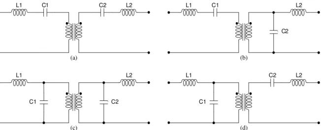
These configurations depend on the way that the passive elements of the resonant tank are connected. The basic resonant circuit topologies are presented in Figure 2.2.
L1 C1 C2 L2 L1 C1
C2 L2
L1 L2 L1 C2 L2
(a) (b)
(c) (d)
C1 C2 C1
These topologies allow galvanic isolation from the input to the output due to the existence of the transformer. Figure 2.2 a) shows the Series-Series topology where in the primary side the inductor B is connected in series with capacitor %B and in the secondary side, the inductor 3 is connected in series with capacitor %3. Figure 2.2 b) shows the Series-Parallel topology where in the primary side the inductor B is connected in series with capacitor %B and in the secondary side, the inductor 3 is connected in parallel with the capacitor %3. Figure 2.2 c) shows the Parallel-Parallel topology where in the primary side the inductor B is connected in parallel with the capacitor %B and in the secondary side, the inductor 3 is connected in parallel with the capacitor %3. Figure 2.2 d) shows the Parallel-Series topology where in the primary side the inductor B is connected in parallel with capacitor %B and in the secondary side, the inductor 3 is connected in series with capacitor %3.
Resonant converters can also allow AC-DC, DC-DC, DC-AC or AC-AC conversion depending on the design of the topology. For example, the DC-DC resonant converter can be obtained by cascading two converters, a resonant inverter (DC-AC converter) connected to a high-frequency rectifier (AC-DC converter). In this case, the DC input power is first converted into AC power by the resonant inverter and then, the AC power is converted back to DC power at the output by the rectifier. To allow isolation, a transformer can be inserted in the converter between the inverter output and the rectifier input. If the converter operates at high-frequency, the overall size of the converter can be reduced (note that a high-frequency transformer is much smaller than a low-frequency transformer) [8].
STATE OF THE ART in two steps, analyzing and designing the rectifier and the inverter separately and, after this, they can be cascaded as in other electronic systems cells/modules.
The cascaded inverter and rectifier need to be compatible with each other. This means that a rectifier requiring an input voltage source (voltage-driven rectifier or voltage-source rectifier) needs to be connected to an inverter whose output behaves like a voltage source (for example, inverters with a parallel-resonant circuit, forcing at the output a sinusoidal voltage). Similarly if the rectifier requires an input current source (current-driven rectifier or current-source rectifier), the inverter output should behave like a current source (for example, inverters with a series-resonant circuit, forcing at the output a sinusoidal current). Finally, to characterize the DC-DC converter, for example, the efficiency or the voltage transfer function, can be both obtained in a simple way as the product of the characteristics of the inverter and the rectifier [8].
Considering this, and in order to be able to design the converter it is considered that the converter will operate at or near resonance. The current and/or voltages are near sinusoidal so, the fundamental-frequency approach or first harmonic approximation (FHA) can be used. This approach considers only the fundamental components of voltage and/or currents (with no harmonic components) [9]. The FHA allows studying and characterizing the behavior of the converter. Nevertheless, note that if the resonant circuit load quality factor (-) is very low and/or the converter is operating far from the resonance (switching frequency 7 much lower or higher than the resonant frequency 8), the current waveforms may differ from sinusoidal waves (current has harmonic components) and the converter may operate in discontinuous conduction mode (DCM). In such cases, if FHA is used, it can lead to inaccurate design of the converter due to non-consideration of the harmonic components. In this case, other design approaches should be considered [8].
In order to design the converter, some considerations need to be accounted for. For example, for higher power density and smaller size power converters the switching frequency needs to be higher. Increasing the switching frequency allows reducing considerably the size of passive elements in the converter circuit, such as transformers, inductors and capacitors. Increasing the switching frequency in typical power converters means higher switching losses. However, using resonant converter topologies allows operating at higher frequencies with low switching losses [9]. In resonant converters, power is transferred in a sinusoidal manner and the switches are softly commutated reducing considerably these losses and noise.
parallel resonant converter (PRC) where the resonant tank is composed by an inductor in parallel with a capacitor. In the SRC shown in Figure 2.3 a), the circuit with the output rectifier and the load is connected in series with the LC resonant tank. In this case, the load behaves as a voltage divider. Acting on the switching frequency of half-bridge inverter changes the impedance of the resonant tank, which in turn changes the converter gain and allows controlling the converter output. Because the load behaves as a voltage divider, the output gain is always equal or lower than 1. At light load (no-load or open-circuit condition), the impedance of the load is very large when compared to the impedance of the resonant tank which makes it difficult to regulate the output of the converter. Theoretically, to regulate the output in light load conditions, the switching frequency should be infinite [9].
Figure 2.3 – Two basic topologies for resonant converters: a) Half-bridge series resonant converter; b) Half-bridge parallel resonant converter [9]
In the PRC shown in Figure 2.3 b), the circuit with the output rectifier and the load is connected in parallel with the resonant circuit. Because the load is connected in parallel, large amounts of circulating current appear. Because of the higher currents it is difficult to use this topology in high power applications [9].
In order to solve these limitations of the typical topologies SRC and PRC, the LLC resonant converter has been proposed in previous literature [9]. This topology has many advantages when compared with typical resonant converter topologies. For example, it allows output regulation, even when variations in the supply or load systems occur, with a small switching frequency variation of the inverter (typical control variable). Because of these advantages, the LLC resonant converter has been used in a high number of applications, from high-density DC-DC converters to low power LED (Light Emitting Diode) drivers [12], [13], or classical 48 V telecom power sources [14].
STATE OF THE ART converter will be considered. More detailed information about batteries will be presented below in this chapter.
Variable Inductor (VI) 2.3.
The proposed converter will be controlled using a new control variable, based on the variable inductance concept. In order to control the converter the operating principle of the VI needs study, especially how the inductance can be regulated in order to control the charging process. In brief this section presents an introduction of the VI, its operating principle for an ETD shaped ferrite core and an explanation of how to regulate the inductance value. In mid-power applications, variable inductors have been researched and used to control the output current of high-frequency resonant circuits [15]. In [16] and [17], a LED driver based on a Resonant Switched Capacitor Converter (RSCC) controlled with a VI is proposed. Some of the previous knowledge presented in the RSCC converter served as reference for this work [18].
VI Principle of Operation 2.3.1.
To understand the operating principle of the VI is necessary to know some basic concepts about inductors. In an inductor the inductance value can be calculated using (2.1).
2
N L=
ℜ (2.1)
where, is the inductance [H], ‚ is the number of turns and ℜ is the core reluctance [A/Wb], which can be calculated as:
0
r e
l A
µ µ
ℜ =
⋅ ⋅ (2.2)
where, N is the length of the core [m], ƒ5 is the magnetic permeability of the core material [H/m], ƒ8 is the magnetic permeability in the vacuum [H/m] (ƒ8 = „ … † …1 ‡ˆ ‰ ) and 12 is the area of the core cross section [ 3].
The voltage across an inductor can be calculated as:
( )
L( )
L
di t
v t L
dt
= ⋅ (2.3)
regulating the core saturation. By controlling this saturation, the magnetic permeability of the core (ƒ5) will change, which causes variation of the core reluctance (ℜ) changing the
inductance value according to (2.1). By changing the DC current on the auxiliary winding, it is possible to control the inductance value on the VI.
The VI used in this work is based on an E shaped core, in particular an ETD ferrite core, as shown in Figure 2.4 a). To build the VI core, two ETD half cores are used which are assembled as in Figure 2.4 b). In the two external arms there is no air gap and, in the middle arm an air gap exists.
Figure 2.„ – VI core: a) ETD shaped core [19]; b) ETD core for VI construction
In VIs based on E-shaped cores there are three windings: two DC control windings and a main AC winding. Figure 2.5 shows the electrical connections of the VI windings and the magnetic flux contributions.
Figure 2.5 – Assembly and Magnetic contribution of the different windings in the VI: a) DC windings assembly and magnetic flux contribution; b) Main winding assembly and magnetic
contribution; c) Complete VI model with DC and main windings assembled [16]
STATE OF THE ART core as shown in Figure 2.5 a) by the black line. Because there is no air gap in the external arms it is easier to saturate this section of the core. By controlling the DC current in the DC windings, !?>, the level of saturation of the core can be controlled which allows control the main AC winding inductance, HE. The yellow area represents the area that is most likely to be saturated by the DC windings.
In Figure 2.5 b) the electric connections of the main AC winding and its magnetic flux contribution is presented. The main AC winding is placed in the middle arm of the core which contains an air-gap in the middle. The air-gap allows decreasing the effective permeability of the core which reduces drastically the magnetic flux density.
In Figure 2.5 c) the general electric connections of the VI is presented as well as the flux directions created by the AC and DC windings. As can be observed there is a common path to both the main and DC flux path that is key for the VI operation [16].
In summary, as response to a DC control current, the global reluctance of the magnetic core is varied, and therefore the differential inductance of the inductor is controlled. Thus, the role of the HE is to change the characteristics of the resonant tank in order to have a controllable output in a similar manner to the classical 7 control. Adding the VI in series with the LLC resonant tank allows changing the resonant frequency and the converter gain. Changing the converter gain in a controlled way allows output regulation.
In this case, the 7 will be kept constant. However, if necessary both control variables might be use simultaneously in order to try to improve the performance and operation of the converter.
Although the VI concept is relatively simple, the equations that are used to explain its behavior and design are quite complex.
The design methodology used for the VI design is presented in the Appendix B. Further information about the VI design methodology, operation and behavior can be found in previous literature [16], [20], [21].
Batteries 2.4.
discharged. Although one of the battery characteristics is the output voltage, it depends on the battery State of Charge (SOC). Figure 2.6 shows the typical discharge curve for a battery as function of the capacity.
2 6 7
*
8 9
8 9
8
# )
9
8
Figure 2.6 – Typical discharge characteristics for batteries [22]
The curve can be divided into three sections. As can be seen, in the first section, if the battery is fully charged the voltage is at its maximum value. When it starts to discharge, the voltage decreases exponentially as represented by the yellow area. This area is more or less wider depending on the battery type. In the second section, the grey area represents the available energy that can be used until the battery voltage reaches its nominal value. In the third section, the battery voltage is below the nominal value and if it continues to be discharged, the voltage drops very quickly.
To charge the battery, a current needs to be injected into the battery which implies that the battery current is negative and the charging follows the characteristics shown in Figure 2.7.
Figure 2.7 – Typical charging characteristics for batteries: a) Lead Acid and Li-Ion batteries; b) Ni-MH and Ni-CD batteries [22]
STATE OF THE ART the starting value, which depends on the SOC, until it reaches the maximum value at which the battery is fully charged. Figure 2.8 shows the problems that can appear during battery charging.
Figure 2.8 – Problems during charging: a) Constant voltage charging; b) Constant current charging [23]
If the charger imposes a constant voltage to charge the batteries, Figure 2.8 a), at the beginning of the charging, the voltage imposed by the charger is higher than the battery voltage. This imposes a very high starting current to feed the batteries, eventually decreasing as the battery charges. Therefore, there is a problem of current spikes in the beginning of the charging process.
If the charger imposes a constant current during the charging process, Figure 2.8 b), the battery will start charging with a controlled current and its voltage increases. When the battery is almost fully charged, if the current is maintained constant the battery voltage will keep increasing achieving possible very high values. Therefore, there is a problem of over-voltages at the end of the charging process.
In conclusion, the ideal charging procedure would start with a constant current and as the battery voltage increases from its initial value (when charging starts) to a value close to the maximum voltage, the charger needs to keep this voltage value under control. From this point on, the battery voltage will increase slowly until reaching its maximum voltage value. This implies that the charging current will decrease naturally to its minimum value, !4_JK4;< (float
Figure 2.9 – Current and voltage of a battery during the charging process [23]
It can be seen that if the charging is controlled as described before there will be no current spikes or over-voltages which contributes to increase the battery life time. In this work, the first charging step with a constant current will be called as the Current Charging Stage (CCS) and the final charging step, which keeps a constant voltage, will be called as the Voltage Charging Stage (VCS). Because the battery voltage is not constant, either during charging or discharging, the battery charger needs to provide a variable DC output.
In the previous paragraphs, the behavior of the batteries during charging and discharging was analyzed. Now it is necessary to address the problem of how much time it takes to fully charge a battery. There are different types of commercial battery chargers for electric vehicles (EV and PHEV), which can be divided in three types [24]:
Normal charging: The charging process is slow, takes about 8 hours. It is used in
domestic applications and the charger is fed by the grid (230 V, 50 Hz, 16 A). The charger is an AC-DC converter that is placed on the vehicle and converts the AC grid power into DC power to charge the batteries.
Fast charging: It is limited by the battery technology and by the power supply. Part of
the converter is outside of the vehicle in the charging station and it is necessary communication between both to have safe charging. The system’s power can go up to 45 kW, which can decrease the charging time to about 30 minutes. In fast charging, the charging station feeds DC power directly to the batteries in the vehicle.
Semi-fast charging: It is similar to the fast-charging but with lower power capacity,
about 22 kW, which increases the charging time but reduces the cost of the charging station.
STATE OF THE ART
Figure 2.10 – Battery charger for EV block diagram [25]
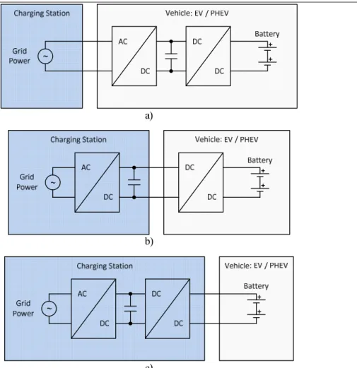
The charging system and the converters can be built in three different ways.
Placed in the vehicle (Figure 2.11 a)). In this case, the charging station feeds the on-board converter from the AC power grid. The charging is controlled in the vehicle by the converter control system. This is used in normal charging systems, with lower power capacities and higher charging times. In this case, the volume of the on-board charger is higher due to the existence of the low-frequency rectifier.
Placed part in the vehicle and part in the charging station (Figure 2.11 b)). This allows faster charging and higher power levels are involved. In this case, the charging station feeds directly the on-board DC-DC converter with DC power and, the on-board module does not need a rectifier as in Figure 2.11 b).
Figure 2.11 – Types of charging systems: a) On-board charger fed by AC power from the grid; b) On-board charger fed by DC power; c) Charger divided between the charging station and the
vehicle; d) Battery charger on the charging station
LLCRESONANT CONVERTER FOR A BATTERY CHARGER
LLC Resonant Converter for a Battery Charger
3.
Chapter 3
3.
In this chapter the LLC resonant converter topology is presented. The electrical scheme is shown; its components and principle of operation are addressed. A theoretical analysis is made and control variables are discussed.
Proposed Battery Charger Application 3.1.
For battery charging applications different converter topologies can be used from simple non-controlled rectifiers to more complex converter topologies with complex control algorithms to improve the converter efficiency and prolong the batteries life time. For the present work, as referred before, a LLC resonant converter will be used to build the battery charger as shown in Figure 3.1:
AC DC AC DC Grid Power Battery VI Control fs Control
Rectifier Transformer High-frequency
rectifier
~
DC Bus
DC-DC Resonant Converter
Rectifier
AC DC Resonant
Inverter AC High-Frequency Rectifier DC (a)
84V – 116V 0 – 10A
(b) DC AC Inverter @100kHz Resonant Tank VI
Figure 3.1 – Battery charger based on the LLC resonant converter block diagram: a) Simple block diagram; b) Block diagram with the block of the LLC resonant converter
followed by a filter capacitor feeds the resonant inverter which works at a constant frequency of 100 kHz. The VI is introduced in the resonant tank. The resonant tank is followed by a high-frequency transformer connected to a high-frequency rectifier. Finally, the batteries are connected at the output of the rectifier. The converter can be controlled using two variables: the switching frequency of the inverter or the VI inductance value. In order to prove the design methodology presented in this work considering both control techniques a simple battery charger application is considered.
For the proposed charger application, Lead-Acid batteries are considered. The battery bank is composed by 16 individual 12 V Lead-Acid batteries, two sets of 8 serially connected batteries in parallel. The nominal voltage of the battery bank is 96 V and can vary between 84 V and 116 V depending on the SOC. The maximum charging current is of 10 A. Each individual battery has a 12 V nominal voltage that can vary between 10.5 V and 14.5 V and the maximum value for the charging current is 5 A.
As described previously (Figure 2.7), the battery voltage does not vary linearly during the charging process. Although this behavior happens in real batteries (Figure 2.9), for the present case study, to simplify the analysis, it will be considered a charging profile where the voltage increases linearly as function of the SOC. Figure 3.2 shows the simplified battery voltage and current profiles and Table 3.1 shows the main design specifications considered for the project of the LLC resonant converter based charger and the characteristics of the battery bank.
Table 3.1 – Design Specifications
Description Specification
Main parameters $EF =400$; 7= 100 ; = 0.5
Battery bank 84$ ≤ $4≤ 116$ ; 0 ≤ !4≤ 101
LLCRESONANT CONVERTER FOR A BATTERY CHARGER
Figure 3.2 – Battery voltage and current profiles and, behavior of HE and 7 values along the
charging process: (a) 7 control and, (b) HE control [29]
Figure 3.2 a) and Figure 3.2 b) show the voltage and current profiles. It is also shown the expected behavior of the control variables, inductance and switching frequency, HE and 7, respectively.
Using the VI control method, the goal is to have a constant charging current, starting with an initial value for HE. Since the battery voltage is not constant, the controller needs to act on the inductance value to compensate the effect of the voltage variation. In this case, as the voltage increases from a minimum value, HE needs to decrease from HE_8 (SOC ~0%), to maintain a constant charging current until an acceptable SOC is achieved (SOC~90% at HE_˜8). This mode is identified as current charging stage, CCS. In the next stage, identified as VCS (voltage charging stage), when the battery is almost fully charged, the voltage needs to be maintained at a constant maximum value as the charging current tends to decrease naturally to its floating level !4_JK4;<. At this point, HE tends to its minimum value HE_B88 (SOC→
100%). During the whole process 7 is kept constant. This simple approach is sufficient to prove the converter performance, however more complex charge control algorithms can be implemented to improve the efficiency of the application itself [29].
Using the frequency control method, the charging profile is similar to the previous one but, in this case, the variable inductor HE is not considered in the circuit and, the resonant inductor role is done by the leakage inductance of the transformer. The control variable is 7. During CCS, 7 varies from 7_8 (SOC ~0%) to, 7_˜8 (SOC ~90%), to maintain a constant charging current as the battery voltage increases. During VCS, 7 tends to its minimum value 7_B88 (SOC → 100%) maintaining the voltage at is maximum value as the charging current tends do its floating level !4_JK4;<.
![Figure 2.1 – Four basic converter configurations: a) AC-DC converter; b) DC-DC converterwith isolation; c) DC-AC converter; d) AC-AC converter [8]](https://thumb-eu.123doks.com/thumbv2/123dok_br/18782923.407192/34.892.187.679.85.288/figure-converter-configurations-converter-converterwith-isolation-converter-converter.webp)
![Figure 2.3 – Two basic topologies for resonant converters: a) Half-bridge series resonant converter; b) Half-bridge parallel resonant converter [9]](https://thumb-eu.123doks.com/thumbv2/123dok_br/18782923.407192/38.892.94.746.406.597/topologies-resonant-converters-resonant-converter-parallel-resonant-converter.webp)
![Figure 2.7 – Typical charging characteristics for batteries: a) Lead Acid and Li-Ion batteries; b) Ni-MH and Ni-CD batteries [22]](https://thumb-eu.123doks.com/thumbv2/123dok_br/18782923.407192/42.892.112.744.726.917/figure-typical-charging-characteristics-batteries-lead-batteries-batteries.webp)
![Figure 2.8 – Problems during charging: a) Constant voltage charging; b) Constant current charging [23]](https://thumb-eu.123doks.com/thumbv2/123dok_br/18782923.407192/43.892.200.739.200.456/figure-problems-charging-constant-voltage-charging-constant-charging.webp)
![Figure 3.2 – Battery voltage and current profiles and, behavior of HE and 7 values along the charging process: (a) 7 control and, (b) HE control [29]](https://thumb-eu.123doks.com/thumbv2/123dok_br/18782923.407192/49.892.155.755.94.285/figure-battery-voltage-current-profiles-behavior-charging-process.webp)

![Figure 3.5 – Typical waveforms of the Half-bridge LLC Resonant Converter [9]](https://thumb-eu.123doks.com/thumbv2/123dok_br/18782923.407192/52.892.254.595.87.502/figure-typical-waveforms-half-bridge-llc-resonant-converter.webp)
![Figure 3.7 – Typical gain curves of LLC resonant converter for various loads and capacitive and inductive region waveforms [26]](https://thumb-eu.123doks.com/thumbv2/123dok_br/18782923.407192/54.892.160.692.275.667/figure-typical-resonant-converter-various-capacitive-inductive-waveforms.webp)
