Ar
ti
cle
*e-mail: [email protected]
Modiication of Silicon Surface with Redox Molecules Derived from Ferrocene
Gonzalo Riveros,*,a Guillermo Gonzálezb and Boris Chornikc
aDepartamento de Química y Bioquímica, Facultad de Ciencias, Universidad de Valparaíso,
Av. Gran Bretaña 1111, Playa Ancha, Valparaíso, Chile
bDepartamento de Química, Facultad de Ciencias, Universidad de Chile, Casilla 653,
Santiago de Chile, Chile
cDepartamento de Física, Facultad de Ciencias Físicas y Matemáticas,
Universidad de Chile, Casilla 487-3, Santiago 8370415, Chile
Este estudo apresenta um método novo para ligar moléculas redox ativas derivadas de ferroceno à superfície de silicone monocristalino. O procedimento consiste na reação de silicone hidrogenado com brometo de alila ativado com luz branca e sua reação subseqüente com monolítio ferroceno para criar uma união covalente entre a molécula redox e a supericie do semicondutor. As camadas formadas são eletroquimicamente ativas e apresentam um processo electroquímico quasi-reversível, atribuído às moléculas de ferroceno ligadas à superfície de silicone. A análise por espectroscopia fotoeletrônica de raios-X (XPS) conirma a presença de moléculas de ferroceno na supericie de silicone.
This study presents a new method to bind active redox molecules derived of ferrocene to the surface of single crystal silicon. The procedure consists in the reaction of hydrogenated silicon with allyl bromide activated with white light and its subsequent reaction with monolithio ferrocene in order to create a covalent union between the redox molecule and the semiconductor surface. The layers formed are electrochemically active and present a quasireversible electrochemical process which is attributed to the ferrocene molecules which are bound to the silicon surface. X-ray photoelectron spectroscopy (XPS) analysis conirms the presence of ferrocene molecules on the silicon surface.
Keyword: silicon, ferrocene, surface modiication, characterization
Introduction
Although molecular electronics appears as a new alternative in the development of nanometric electronic
devices,1 the production of transistors and other electronic
devices is still dominated by silicon technology. Contributions to the transition between both technologies centered in the development of hybrid
semiconductor-molecule materials are therefore of paramount importance.2
In this ield, there are several studies referring to the preparation and redox property studies of self-assembled monolayers (SAMs) on silicon surfaces. The formation of SAMs on oxidized silicon surfaces has been well
documented.3-5 However, the Si–O bond is in general
unfavorable for electronic applications because of a
generally poor molecule-electrode electron transfer. Much better results are obtained in absence of the oxide layer
through a direct Si–C union linkage.6
The formation of the Si–C bond has been usually
performed by ultra high vacuum (UHV) techniques,7-9 or
by radicalary processes.3,9 The latter have been studied
more thoroughly due to the relatively low operation cost. The general mechanism of these reactions involves the
double bond addition to the Si–H surface,9 where double
bond homolytic cleavage is achieved by reaction with
peroxides,10 by UV irradiation,11 by thermal activation,12 by
electrochemical processes,13,14 or more recently, by white
light irradiation.15-18 The union of electroactive molecules
the development of charge storage devices (i.e. capacitors),
in which the charge is stored within the stable redox states of the molecule, leading to high charge density, higher
than the conventional SiO2 capacitors. Furthermore, the
charge storage properties are dependent on the molecule, allowing for charge-retention in a time range of minutes and
hours.2 However, it is not always easy to have electroactive
molecules appropriately functionalized with an unsaturated alkyl chain. Commercially available ferrocene precursors
as those used by Decker and co-workers,15-17 and Li
and co-workers19-21 are scarce, limiting the number of
the studied systems. A different route is followed by
Fabre and Hauquier 22 who attach an amine-substituted
ferrocene derivative to a pre-assembled acid-terminated alkyl monolayer through several chemical steps. Good stability and high coverage of electroactive molecules can be obtained using this method.
Another method is to synthesize an electroactive molecule capable of generating a covalent bond with the
silicon surface. Thus, Bocian, Lindsey and co-workers.23-25
have synthesized a great number of porphyrins and triple-decker sandwich compounds that can be linked to gold and silicon surfaces. However, the synthesis, separation and characterization of these compounds are complicated and dificult to carry out.
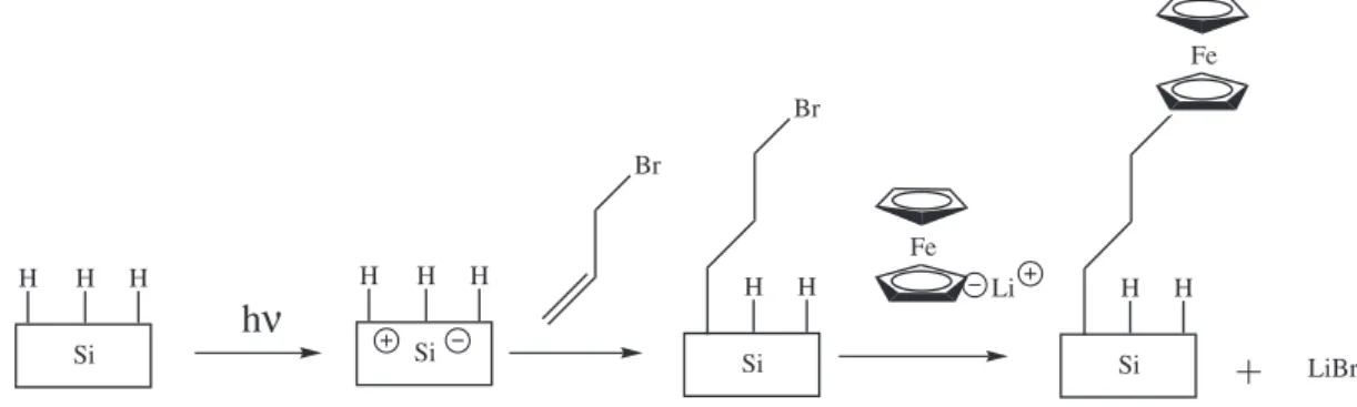
Thus, this study introduces the development of a simple and versatile method for the functionalization of silicon surfaces with electrochemically active ferrocene molecules bound to the substrate by covalent Si–C bonds. This procedure involves a hydrosilylation reaction activated by white light between allyl bromide and the hydride-terminated silicon surface, and, the subsequent reaction of this modiied surface with monolithio-ferrocene. The insertion of a double bond to the Si–H surface activated by white light has been previously studied and has shown to be an ideal method for the Si–C bond formation. However, the union of the ferrocene molecule through the reaction between the monolithio-ferrocene and the bromide terminal chain has not been reported. The advantage of this new
procedure is that it facilitates the development of a great variety of products with different properties offering the possibility to prepare tailor-made electroactive materials;
i.e. to control the distance between the redox center of the
electroactive molecules and the semiconductor surface by using an appropriate alkenyl bromide precursor.
Experimental
Silicon cleaning
Previous to the synthesis, the formation of a reactive Si–H surface is necessary. In order to do this, the silicon wafers (International Wafer Service Inc., (100), p-type,
5-10 Ω cm) were cut with diamond and cleaned with
a piranha solution (concentrate H2SO4 and H2O2 3:1 in
volume) at 60 °C during 40 min. Next, the samples were rinsed with deionizated water and treated with diluted HF (2-4%). Finally, the samples were rinsed with deionizated water, dried under argon low and deposited in a dry-box.
Reaction with allyl bromide
The silicon samples were covered with a thin ilm of allyl bromide (Aldrich) and illuminated with white light (halogen lamp, 20 W) for 1 h. The modiied samples were thereafter rinsed several times with dichloromethane to eliminate the excess of non-reacted allyl bromide.
Reaction with monolithio ferrocene
The monolithio ferrocene was synthesized according
to Goldberg et al.26 and Rebiere et al.27 It was used
immediately in the same solution. The silicon samples modiied with allyl bromide were put in contact with a solution of monolithio ferrocene during 1 h. The reaction between them is similar to that reported in the formation
of alkyl ferrocenes reaction.28 Figure 1 shows the diagram
for the silicon modification developed in this study.
H H H
Si
H H H
Si
h
ν
H H
Si
Fe
Li H H
Si LiBr
Br
Br
Fe
Following this, the samples are retired and rinsed with dichloromethane and acetonitrile.
Analysis and characterization
All electrochemical measurements were performed in a conventional cell with three electrodes: a working electrode (silicon modiied sample), a counter electrode (platinum
wire) and a reference electrode (Ag/Ag+, E = 0.681 V vs
NHE). All the potentials shown in this study are in reference to the reference electrode. A special Telon holder was made for the working electrode. The silicon sample was placed inside the holder and sealed with a stainless steel rod covered with Telon. The electric contact between the silicon sample and the stainless steel rod was done with a Ga/In eutectic. In every case, the electrode exposed area
was 0.196 cm2.
A 0.1 mol L-1 tetraethylammonium perchlorate in
dry acetonitrile was used as an electrolitic solution. The voltammetric measurements were performed in a potentiostate-galvanostate AUTOLAB model PGSTAT 12. XPS measurements were done with a Perkin Elmer 1257 electron spectrometer which included an ultra high vacuum chamber and a hemispherical electron energy analyzer. The X-ray source has two anodes: Al and Mg, providing uniltered 1486.6 eV and 1253.6 eV photons,
respectively, which belong to the main Kα line. Binding
energy calibration was done using the peak of adventitious carbon, ixing it at 284.8 eV.
The morphology of the modiied samples was analyzed by Atomic Force Microscopy (AFM) employing a Digital Instrument (Nanoscope IIIa series) in tapping mode.
Results and Discussion
Electrochemical characterization
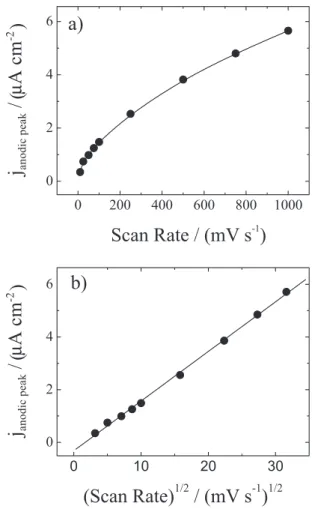
Once modiied, the silicon samples were analyzed by cyclic voltammetry. This analysis was carried out inside a dry-box to avoid oxidation of the silicon surface. Figure 2 shows the voltammetric response of the silicon sample modiied with propyl ferrocene at different scan rates.
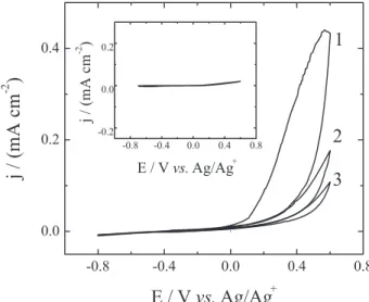
As shown in Figure 2, there is a quasireversible electrochemical process attributed to the ferrocene molecule linked to the silicon surface by the alkyl chain. No other redox process can be observed. Furthermore, in the voltammetric responses of a clean silicon electrode without modification (Figure 3), only one oxidation process due to electrode oxidation can be observed. The oxide formation is the responsible of the electrode passivation observed when successive scans are carried
out. In the case of the silicon electrode modiied with allyl bromide (inset Figure 3), a more resistive response without oxide formation can be observed. This response can be due to two factors: The stable Si–C bond formation without a terminal active molecule that acts like a barrier between the electron surface and the electrolyte, and the oxide formation during the modiication process of the silicon surface with allyl bromide. For this electrode, no passivation could be observed when successive scans were carried out. This probes that the organic layer as well as the oxide layer protect the semiconductor surface against your posterior oxidation. A conirmation of the oxide formation on the silicon surface is discussed in the XPS and AFM analysis.
Thus, the responses observed in Figure 2, are attributed only to the active redox molecules of propyl ferrocene
Figure 2. Cyclic votammogram of p–Si (100) electrode functionalized with propyl-ferrocene at different scan rates (25, 50, 75 and 100 mV s-1).
Solution of 0.1 mol L-1 tetraethylammonium perchlorate in dry acetonitrile.
Figure 3. Voltammetric response of clean p–Si–H (100) without
covering only a fraction of the silicon surface. Also, the organic monolayer of propyl ferrocene coating the silicon surface is robust and chemically stable under these working conditions, because the electrochemical response remains unalterable even after successive scans. On the other hand, the difference between the anodic current peak and cathodic
current peak (∆Ep = Epa– Epc) is higher than 59/n mV. This
difference increases as increases the scan rates, from
∆Ep = 150 mV (scan rate of 25 mV s–1) to ∆Ep= 210 mV
(scan rate of 100 mV s–1). The above conirm that the process
studied is a quasireversible electrochemical process. By means of a deconvolution (using asymmetric Gaussian peaks for the quasireversible electrochemical processes) to decompose the anodic electrochemical process and the integration of the voltammetric curve corresponding to the redox process, it is possible to obtain the total number of active molecules linked to silicon. The results of this integration give a range between
3.67×10⁻¹¹ – 4.80×10⁻¹¹ mol cm–2 of active molecules
on the silicon surface. Considering the diameter of a propyl ferrocene molecule (6.40 Å), the lattice spacing of silicon (5.43 Å), the silicon atomic radio (1.32 Å) and the distribution of the atoms in a (100) crystallographic orientation, it is possible to establish the optimum coverage for the silicon surface with electroactive molecules. According to this, one propyl ferrocene molecule bonded to one silicon atom, cover four supericial atoms of silicon. Due to the esteric effect of the ferrocene molecule, is not possible to bond another ferrocene molecule in each one of these four silicon atoms. Considering the above mentioned, the coverage of our modiied silicon surface were between 13-17% of redox molecules. This quantity indicates that the surface is not covered totally by active molecules, being this less than a monolayer. Although the coverage is lower than other reports employing similar molecules, this method permits the variation of the length silicon-molecule changing the alkene halide employed in the synthesis process. Thus, the method proposed allows several studies of the electric properties of the system with the distance between the electrode and the redox center. However, higher coverage would be possible with a more
precise control of the experimental conditions, i.e., the
humidity and oxygen control of the dry-box.
Figure 4 shows the anodic peak variation with the scan rate and square root of scan rate. According to accepted theory, in the case of adsorbed molecules, the variation of current peaks (anodic and/or cathodic) is linear with the scan rate. On the other hand, in the case of molecules in solution, the variation of the current peaks is linear with the square root of scan rate. In both cases a reversible electrochemical process is considered.
In these experiments, only a linear relationship was obtained between the anodic current peak and the square root of scan rate (Figure 4b). We recorded a voltammogram with a gold electrode in the same electrolytic solution employed in the above experiments in order to discard any interference of molecules in solutions. This did not show any electrochemical process and only capacitive current could be observed. The latter conirms that the electrochemical process depicted is caused by molecules attached to the silicon surface.
On the other hand, this anomalous relationship has been previously reported for vinylferrocene molecules
linked to porous silicon electrodes,29 but not has been
observed when these molecules were linked to the lat
silicon surface.15 Numerous studies have been carried out
to understand the interfacial processes during the electron transfer in redox self-assembled monolayers. Effects of
interfacial solvation,30 double layer and interfacial potential
distribution,30,31 ion-pairing formation,32 chain length,33
solvent,33,34 intermolecular interactions between different
functional groups,35 and permeability,36 have been studied
in this ield, but the behavior described in our work has not been reported.
An approach to describe this anomalous behavior is carried out by applying the model developed by Blauch
and Savénat.37 They relate the physical displacement
and electron hopping in the charge transport through supramolecular redox systems within 2D and 3D systems. In this model, two limit behaviors are possible: When physical motion is either nonexistent or much slower than the electron hopping, the charge transport becomes a percolation process; on the other hand, if the molecular motion is faster than the electron hopping, a mean-ield behavior is observed. The latter approximation is particularly valid for system in which the redox centers are irreversibly attached to the supramolecular structure,
but are not strictly immobile: i.e. bounded diffusion. In this
case, the so called Laviron-Andrieux-Savéant equation is put into effect.
(1)
Dap is the apparent diffusion coeficient, kex is the
bimolecular rate constant for electron self-exchange
(electron hopping), CE is the total concentration of redox
species and ∆x is the center-to-center distance between
redox centers. Thus, the apparent diffusion coeficient is determined only by the electron hopping between the redox molecules and the distance between them.
Thus, in our system, the charge transport would take place via electron hopping between the neighboring ferrocene molecules. However, the ferrocene molecules are not adjacent one to another but rather, are separated by a certain distance. The space between molecules would permit a fast molecular motion, thus reaching a situation of bounded diffusion, in which the motion of irreversibly attached molecules is greater than the electron hopping and where the range of bounded diffusion is suficiently ample so as to allow for interactions between neighboring redox centers. This way, the electrochemical process is limited by the electronic transport between ferrocene molecules through electron hopping, thus reaching a diffusion situation. This hypothesis is consistent with the low coverage obtained in this study. This low coverage could be caused by the high volatility of allyl bromide. During the silicon modiication, a great quantity of this compound is evaporated as a result of the heat of the lamp employed, exposing the silicon surface to the dry box atmosphere. To avoid the total evaporation of this compound during the modiication process, the allyl bromide is continuously added on the silicon surface. However, the decrease in the amount of allyl bromide within the silicon surface
during the modiication step would avoid its total surface modiication.
In order to conirm the above mentioned, experiences with vinyl ferrocene were carried out, similar to those in
referring literature.15-17 Because vinyl ferrocene has a higher
boiling point than allyl bromide, it doesn’t evaporate during the silicon modiication, and therefore facilitates the Si–C bond formation. Furthermore, the silicon sample needs to be over 60 °C to keep this compound melted. Thus, the activation is achieved thermically and in a lesser degree through white light, thus favoring the surface modiication. On the other hand, the melted vinyl ferrocene layer becomes a protective layer against any oxidation process. Analyses carried out by cyclic voltammetry (Figure 5a) show a larger amount of active molecules attached to the silicon surface than those in the modiied samples in the proposed method of this study reaching values close to one monolayer. In this situation, the molecules don’t present any motion
Figure 5. a) Cyclic voltammogram of p–Si (100) electrodes functionalized
with vinyl ferrocene (continuous line) and propyl ferrocene (dotted line) at the same scan rate (100 mV s–1). Solution of 0.1 mol L-1
and the distance between active redox centers is small,
thus a percolation process prevails (Dap ca. 0). In fact, in
this system, the variation of the anodic current peak is linear with the scan rate and not with the square root of the scan rate as in our systems (Figure 5b). Furthermore, this experience conirms that the diffusion process observed in our system is not a product of the silicon substrate because the latter acts as a metallic electrode.
XPS analysis
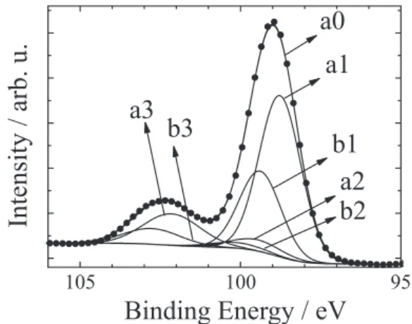
XPS measurements were carried out to conirm the presence of ferrocene molecules attached to the silicon surface through the propyl chain. Figure 6 shows a high resolution XPS spectrum of a silicon sample modiied with propyl ferrocene in the Si 2p region. For curve itting in this spectrum we used a model with three peaks (three different adjustable values for the chemical shift) and considered that each Si 2p line is a doublet because of spin-orbit splitting. Therefore, the curve itting calculation involves six peaks but the free parameters are only for three peaks, because all
the 2p1/2 levels are constrained to have 0.6 eV higher binding
energy than the corresponding 2p3/2 levels, and the peak
areas of the 2p1/2 levels are exactly ½ of the corresponding
2p3/2 levels. Besides, both levels have the same line width
and the same proportion between gaussian and lorentzian
functions. The result of this itting is (Figure 6): 2p3/2 levels
located at 98.8 eV. (a1), 99.5 eV (a2) and 102.1 eV (a3). The
2p1/2 levels (b1, b2 and b3) do not provide any additional
information and are not used for identiication.
The peak at 102.1 eV (a3) corresponds to oxidized
silicon, in agreement with Dreiner et al.38 We believe
that in our experiment, it is produced during or after the
modiication process, as reported by Karadas et al.39 The
presence of silicon oxide is not rare in this type of sample, as demonstrate the results obtained by other authors in
similar conditions.15,16 Furthermore, the peak observed at
98.8 eV (a1), corresponds to the Si–Si bond present in the
bulk of the sample, in agreement with Cardinaud et al.40
Peak a2 can be assigned to Si(+1).38 This signal can be
interpreted as a Si–C bond or as a Si–H bond, but the
latter can be disregarded because of SiO2 formation (as
indicated above).
Figure 7 shows the XPS spectrum for the Fe 2p region. A curve itting calculation gives three peaks, located at 707.7 eV (a1), 709.9 eV (a2) and 714.8 eV (a3). Following
Fischer et al.41 measurements, peak a1 can be ascribed
to ferrocene molecules. On other hand, peak a2 may correspond to Fe(III) species derived from ferrocene. The presence of Fe (III) species is not rare in this type of sample and could be the result of ferrocenium molecules
resulting from the manipulation of the samples,15-17 or from
the exposition of ferrocene molecules to X-rays.42 Peak a3
at 714.8 eV is attributed to a shake-up satellite of a2.
Thus, through XPS analysis, the presence of ferrocene molecules on the silicon surface is conirmed.
AFM analysis
Figure 8 shows the AFM images obtained from a silicon sample before and after the modification with propyl ferrocene at different magniications. In the irst case, a relatively smooth surface is observed. Additionally, a little granular oxide formation can be appreciated due to the fact that the measurements are carried out in air and not in a dry box (Figures 8a and 8b). On the other hand, the sample modiied with propyl ferrocene shows a different morphology, which is more homogeneous than the silicon Figure 6. XPS spectrum in the Si 2p region for a silicon sample modiied
with propyl ferrocene. Dots are experimental measurements and lines are curve itting calculations. Peaks a1, a2 and a3 are 2p3/2 states and peaks b1, b2 and b3 are 2p1/2 states. Line a0 is the sum of all the above plus the background.
Figure 7. XPS spectrum in the Fe 2p region for a silicon sample modiied
sample without modiication and that not correspond to the granular silicon oxide (Figures 8c and 8d). Possibly, the stable Si–C bond formed on the silicon surface, avoid the oxide formation. However, the surface is not smooth and a certain domains can be observed (Figure 8c). These domains are formed during the silicon modiication, but don’t correspond to the propyl ferrocene, because the section analysis is not consistent with the dimensions of this molecule. These domains can be attributed to the possible polymerization of the alkene chain on the silicon surface during the activation step. This is consistent with the low coverage observed in this study.
Conclusions
In this study, the surface silicon modiication with molecules that derived from ferrocene has been proven. The reaction was carried out with silicon and allyl bromide and finally with monolithio ferrocene. This process allows a route more versatile than the use of commercial products (vinylferrocene) allowing to control the distance between the redox molecule and the semiconductor surface by means of the alkene halide utilized in the synthesis proposed. The molecules anchored showed a quasireversible electrochemical response. A bounded diffusion and electron hopping model are used to explain the unusual relationship between the anodic current peak and the square root of the scan rates. This model is consistent with the results observed in the AFM images. XPS analysis of the Si 2p and Fe 2p3/2 regions are consistent with the presence of ferrocene molecules on the Si surface.
Acknowledgment
This work has been supported by FONDECYT (Chile) Project, No. 1050700.
References
1. Metzger, R. M.; Chem. Rev.2003, 103, 3803.
2. Kuhr, W. G.; Electrochem. Soc. Interface2004, 13, 34. 3. Ulman, A.; Chem. Rev.1996, 96, 1533.
4. Younkin, R.; Berggren, K. K.; Johnson, K. S.; Prentiss, M.; Ralph, D. C.; Whitesides, G. M.; Appl. Phys. Lett.1997, 71,
1261.
5. Masuda, Y.; Sugyama, T.; Lin, H.; Seo, W. S.; Koumoto, K.;
Thin Solid Films2001, 382, 153.
6. Kar, S.; Miramond, C. ; Vuillaume, D.; Appl. Phys. Lett.2001,
78, 1288.
7. Forrest, S.; MRS Bull.2001, 26, 108.
8. Forrest, S. R.; Chem. Rev.1997, 97, 1793. 9. Buriak, J. M.; Chem. Rev.2002, 102, 1271.
10. Lindford, M. R.; Chidsey, C. E. D.; J. Am. Chem. Soc. 1993,
115, 12631.
11. Cicero, R. L.; Chidsey, C. E. D.; Langmuir2002, 18, 305. 12. Sieval, A. B.; Linke, R.; Heij, G.; Meijer, G.; Zuilhof, H.;
Sudhölter, E. J. R.; Langmuir2001, 17, 7554.
13. Teyssot, A.; Fidélis, A.; Fellah, S.; Ozanam, F.; Chazalviel, J.
N.; Electrochim. Acta2002, 47, 2565.
14. Allongue, P.; de Villeneuve, C. H.; Pinson, J.; Ozanam, F.; Chazalviel, J. N.; Wallart, X.; Electrochim. Acta1998, 43, 2791. 15. Zanoni, R.; Cataruzza, F.; Coluzza, C.; Dalchiele, E. A.; Decker, F.; Di Santo, G.; Flamini, A.; Funari, L.; Marrani, A. G.; Surf. Sci.2005, 575, 260.
16. Dalchiele, E. A.; Aurora, A.; Bernardini, G.; Cattaruzza, F.; Flamini, A.; Pallavicini, P.; Zanoni, R.; Decker, F.;
J. Electroanal. Chem.2005, 579, 133.
17. Decker, F.; Cattaruzza, F.; Coluzza, C.; Flamini, A.; Marrani, A. G.; Zanoni, R.; Dalchiele, E. A.; J. Phys. Chem. B2006, 110, 7374.
18. Sun, Q. Y.; de Smet, L. C. P. M.; van Lagen, B.; Wright, A.; Zuilhof, H.; Sudhölter, E. J. R.; Angew. Chem., Int. Ed.2004,
43, 1352.
19. Li, Q.; Mathur, G.; Homsi, M.; Surthi, S.; Misra, V.; Malinovskii, V.; Schweikart, K. H.; Yu, L.; Lindsey, J. S.; Liu, Z.; Dadke, R. B.; Yasseri, A.; Bocian, D. F.; Kuhr, W. G.; Appl. Phys. Lett.
2002, 81, 1494.
20. Zhao, Q.; Luo, Y.; Surthi, S.; Li, Q.; Mathur, G.; Gowda, S.; Larson, P. R.; Johnson, M. B.; Misra, V.; Nanotechnology2005,
16, 257.
21. Li, Q.; Surthi, S.; Mathur, G.; Gowda, S.; Misra, V.; Sorenson, T. A.; Tenent, R. C.; Kuhr, W. G.; Tamaru, S.; Lindsey, J. S.; Li, Z.; Bocian, D.; Appl. Phys. Lett.2003, 83, 198.
Figure 8. AFM images of silicon samples without [(a), (b)] and modiied
with propyl ferrocene [(c), (d)]. (a) anb (c) images: 1 µm × 1 µm; (c) and
22. Fabre, B.; Hauquier, F.; J. Phys. Chem. B2006, 110, 6848. 23. Liu, Z.; Yasseri, A. A.; Loewe, R. S.; Lysenko, A. B.;
Malinovskii, V. L.; Zhao, Q.; Surthi, S.; Li, Q.; Misra, V.; Lindsey, J. S.; Bocian, D. F.; J. Org. Chem.2004, 69, 5568.
24. Carcel, A. M.; Laha, J. K.; Loewe, R. S.; Thamyongkit, P.; Schweikart, K. H.; Misra, V.; Bocian, D. F.; Lindsey, J. S.;
J. Org. Chem.2004, 69, 6739.
25. Balakumar, A.; Lysenko, A. B.; Carcel, C.; Malinovskii, V. L.; Gryko, D. T.; Schweikart, K-H.; Loewe, R. S.; Yasseri, A. A.; Liu, Z.; Bocian, D. F.; Lindsey, J. S.; J. Org. Chem. 2004,69,
1435.
26. Goldberg, S. I.; Keith, L. H.; Prokopov, T. S.; J. Org. Chem.
1963, 28, 850.
27. Rebiere, F.; Samuel, O.; Kagan, H. B.; Tetrahedron Lett. 1990,
31, 3121.
28. Dietz, S. D.; Bell, W. L.; Cook, R. L.; J. Organomet. Chem.
1997, 545-546, 67.
29. Bateman, J. E.; Eagling, R. D.; Worrall, D. R.; Horrocks, B. R.; Houlton, A.; Angew. Chem., Int. Ed.1998,37, 2683.
30. Rowe, G. K.; Creager, S. E.; J. Phys. Chem.1994, 98, 5500.
31. Smith, C.P.; White, H. S.; Anal. Chem.1992, 64, 2398.
32. Rowe, G. K.; Creager, S. E.; Langmuir 1991, 7, 2307. 33. Rowe, G. K.; Creager, S. E.; Langmuir1994, 10, 1186.
34. Acevedo, D.; Abruña, H. D.; J. Phys. Chem.1991, 95, 9590. 35. Guo, Y.; Zhao, J.; Zhu, J.; Thin Solid Films2008, 516, 3051.
36. Hockett, L. A.; Creager, S. E.; Langmuir 1995, 11, 2318. 37. Blauch, D. N.; Savèant, J. M.; J. Am. Chem. Soc.1992, 114,
3323.
38. Dreiner, S.; Schürmann, M.; Westphal, C.; Zacharias, H.; Phys.
Rev. Lett.2001, 86, 4068.
39. Karadas, F.; Ertas, G.; Suzer, S.; J. Phys. Chem. B2004, 108,
1515.
40. Cardinaud, C.; Lemperière, G.; Peignon, M. C.; Jouan, P. Y.;
Appl. Surf. Sci.1993, 68, 595.
41. Fischer, B.; Wrighton, M. S.; Umana, M.; Murray, R. W.;
J. Am. Chem. Soc.1979, 101, 3442.
42. Zheng, F.; Pérez-Dieste, V.; McChesney, J. L.; Luk, Y. Y.; Abbott, N. L.; Himpse, F. J.; Surf. Sci. Lett.2005, 587, L191.
![Figure 8. AFM images of silicon samples without [(a), (b)] and modiied with propyl ferrocene [(c), (d)]](https://thumb-eu.123doks.com/thumbv2/123dok_br/18994686.461820/7.892.99.436.117.399/figure-afm-images-silicon-samples-modiied-propyl-ferrocene.webp)
