Thesis presented to
universidade federal de minas gerais as partial requirement for the title of
phd in physics Instituto de Ciências Exatas
Departamento de Física
© June2016
supervisor:
Prof. Dr. Paulo Sergio Soares Guimarães Departamento de Física
Instituto de Ciências Exatas
Universidade Federal de Minas Gerais Belo Horizonte, Brasil
co-supervisor:
Prof. Dr. Dario Gerace Dipartimento di Fisica
Università degli Studi di Pavia Pavia, Italia
location:
expansion approach. We find that when the quantum dots are in res-onance with either of the two lowest energy modes (bonding/anti-bonding) of the photonic dimer, and in the strong cavity-cavity cou-pling regime, the inter-dot radiative coucou-pling strength is proportional to the quality factors of the dimer modes and it can be of the order of 1 meV, which is at least an order of magnitude larger than typi-cal values achieved in one-dimensional systems. We also address the effects of structural disorder in the photonic crystal lattice on the mu-tual coupling between the two quantum dots, by assuming disorder parameters that are consistent with the current state-of-art fabrication technology. We find that the effective radiative coupling between the dots is robust against non-perfect quantum dot positioning and, to a smaller extent, to structural disorder in the photonic crystal. Using a fully quantum mechanical model, based on the master equation, we quantify the entanglement between the quantum dots by the Peres-Horodecki negativity criterion. We show that it is possible to achieve negativity values of the order of 0.1(20% of the maximum value) in the steady sate regime, for interdot distances which are larger than the characteristic wavelength of the system. We also find that this amount of entanglement remains of the same order of magnitude, as long as the distance between the dots is such that the normal mode splitting of the photonic dimer is much greater than the normal mode linewidth. Considering detuned quantum dots, we find that the en-tanglement is preserved as long as the dot-dot detuning is smaller than the exciton linewidth. Finally, we determine that the most ap-propriate configuration for long-range entanglement applications is the one for which the line connecting the centers of the L3 cavities is at an angle of 30 degrees with the horizontal axis. Based on this configuration, we propose a simple device for practical applications in the transient dynamics where the amount of entanglement can be of the order of40% for state-of-art InGaAs quantum dots.
state entanglement between distant quantum dots in photonic crystal dimers”,Submitted to Physical Review B.
years, by his generous support in the theoretical and very technical aspects of my Doctoral research. His scientific work served as inspi-ration for many topics of the present thesis.
Special thanks to my dear friend Prof. Herbert Vinck Posada who is supporting me since my first scientific works on photonic crys-tals and gave me several insights in the first stage of my Doctoral work. Also, I would like to acknowledge the invaluable support of Prof. Marcelo França Santos in the quantum mechanical aspects of the present work.
Thanks to my friend Dr. Carlos Parra for useful discussions during the quantum mechanical calculations which were carried out in the last part of this thesis.
I would like to thank the team of the Laboratory of Semiconductors (UFMG) for their friendship and very nice working atmosphere.
Finally, I would like to acknowledge the financial support for this work, from CAPES, CNPq, FAPEMIG and INCT-DISSE.
2.2.2 Förster coupling between two quantum dots 24 2.3 Semiconductor quantum dots in photonic crystals 25
2.3.1 Semiclassical formalism 26 2.3.2 Quantum formalism 30 3 results 37
3.1 Photonic crystal molecule 38
3.2 Long-distance radiative coupling between quantum dots 41 3.3 Disorder effects on the radiative coupling between
quan-tum dots 45
3.4 Long-range entanglement between radiatively coupled
quantum dots 49
4 conclusions 59 a supercell method 63 bibliography 67
duced the idea of strong Anderson localization of photons in dis-ordered dielectric systems, by fluctuating a periodic dielectric func-tion in a superlattice with a random dielectric contribufunc-tion [2]. Due to these important works, nowadays 1987 is known as the birthday of photonic crystals, namely, periodic spatially-modulated dielectrics, with potential capabilities of controlling the flow of light. Photonic crystals, schematically represented in Fig. 1, can be periodic in one, two or three dimensions, allowing the engineering of the electromag-netic density of states throughout the dielectric structure [3]. In partic-ular, two-dimensional photonic crystals embedded in planar semicon-ductor dielectric waveguides, i.e., two-dimensional photonic crystal slabs, have emerged as the best candidates for on-chip implementa-tions due to the high-nanometric precision of lithography and etching processes achieved nowadays [4,5]. On the other hand, semiconduc-tor quantum dots have attracted considerable attention in the last two decades, because they are promising candidates to realize solid state quantum bits (qubits) to be employed in quantum information and communication technologies [6, 7]; their characteristic discrete spec-tra, long coherence times, and large oscillator strengths make them almost ideal artificial atoms that can be fixed in position and inte-grated into semiconductor structures [8,9]. Interfacing photonic crys-tals with semiconductor quantum dots have allowed to study a vast variety of cavity quantum electrodynamics phenomena [10, 11, 12], quantum information technologies [13] and quantum photonic ap-plications [14, 15]. Specifically, fully quantum mechanical effects as strong light-matter coupling [16,17] and control of spontaneous emis-sion [18,19] have been successfully demonstrated in photonic crystal cavities due to their capabilities of confining the light with modal vol-umes next to the diffraction limit and very high quality factors [20].
The realization of two coherently interacting quantum dots and the possibility to externally control such interaction are crucial require-ments to perform two-qubit operations, which are the building blocks of a quantum information protocol [22]. Nevertheless, the interaction strength between two quantum dots decays rapidly as a function
Figure1: Schematic illustration of one, two and three dimensional periodic-ity in photonic crystals. Figure taken from Ref. [21].
of the inter-dot distance [23], which makes entanglement challeng-ing when their distances are larger than their characteristic emission wavelength. Thus, there is a growing theoretical and experimental interest to mediate the dot-dot coupling via electromagnetic modes in a semiconductor photonic crystal structure [24, 25, 26], enabling controlled gate operations with such interacting qubits through a
photonic quantum bus, namely, a photonic degree of freedom which interacts with the localized qubits. Due to the exceptional capabil-ities to efficiently guide and confine the electromagnetic radiation, and the high degree of precision in fabrication techniques currently achieved, photonic crystal slab structures should allow to overcome the short-range Förster coupling between interacting quantum dots, thus achieving sizable effective radiative coupling at distances quite larger than their emission wavelength. Proposals for increasing the mutual interaction distance between two quantum dots in a photonic crystal platform mainly considered using a waveguide as a bus for photon propagation [26, 27, 28]. The role of structural disorder on light localization was also addressed [29]. Alternatively, preliminary studies considered the mutual coupling between two quantum dots positioned at the field antinodes within the same photonic crystal cav-ity [26,30], for which early experimental evidence was shown [24,31]. The possibility of mediating the inter-dot coupling through the nor-mal modes of a photonic molecule has been considered for coupled micro disks [32], where the distance is limited by evanescent inter-cavity coupling in free space.
two strongly coupled photonic crystal (PC) nanocavities, each con-taining a single quantum dot (QD). The distance between the nanocavities,dc, can be larger than the characteristic exciton emis-sion wavelength in vacuum,λ0.
the coupling strengths between each dot and the field, or the total (intrinsic and extrinsic) photonic mode and exciton loss rates. The for-mer quantity increases as the modal volume decreases, for two quan-tum dots that are spatially positioned at an electric field antinode of the corresponding photonic mode, and the latter should be small as compared to the exciton-field coupling strengths. Photonic crys-tal molecules naturally fulfill these required conditions. In fact, the normal modes associated to photonic crystal molecules are strongly localized in the photonic cavities, allowing modal volumes next to the diffraction limit, and quality factors can be even larger (i.e., smaller losses) than the quality factors of the decoupled cavities [34]. In ad-dition, it has been recently shown that it is possible to have strongly coupled photonic crystal cavities at inter-cavity distances which are quite larger than the characteristic wavelength of the system in a pho-tonic crystal molecule [35]. A schematic representation of our system is shown in Fig. 2. The photonic molecules we are interested in are composed of two coupled nominally identical photonic crystal slab cavities, i.e., photonic crystal dimers.
2.1 theory of photonic crystals
The electronic transport in atomic or molecular crystals is determined by the geometry of the underlying Bravais lattice and the physical properties of the atomic basis. As it is well known from solid state physics, electrons suffer coherent scattering when the period of the lattice and the size of the atomic basis, determined by the atomic po-tential, is of the order of their de Broglie wavelength. These scattered waves can interfere, giving rise to allowed (constructive interference) and forbidden (destructive interference) states. The former are known as electronic bands and the latter as electronic band gaps. Similarly, electromagnetic waves suffer coherent scattering in periodic dielec-tric media when the period of the lattice and the dielecdielec-tric dimensions are of the order of the electromagnetic wavelength. Here, constructive and destructive interference of the scattered waves determine the pho-tonic bands and phopho-tonic band gaps of the system, respectively. Such structures, whose dielectric function is periodically modulated, are known as photonic crystals, and they are a subject of study of electro-magnetic theory, applying methods and concepts usually employed in quantum mechanics.
2.1.1 Maxwell’s equations in periodic dielectric media
The starting point of every study on photonic crystals is determined by the formulation of the problem in terms of the fundamental equa-tions of the electromagnetic theory, i.e., Maxwell’s equaequa-tions. Since we are mainly interested in the spectrum of the system instead of its physical response, we assume that free charges and electric currents are absent. Under these assumptions, Maxwell’s equations take the following form in Gaussian units:
∇ ·D(r,t) =0, ∇ ×E(r,t) = −1
c ∂
∂tB(r,t),
∇ ·B(r,t) =0, ∇ ×H(r,t) = 1
c ∂
∂tD(r,t), (1)
whereE,H,DandBare the electric, magnetic, electric displacement and magnetic induction fields, respectively, andcis the speed of light in vacuum. The electromagnetic fields Hand B, as well as Eand D are related by the constitutive relations [36]:
B(r,t) =µˆ(r)H(r,t), D(r,t) =ǫˆ(r)E(r,t), (2) where ˆµ(r) and ˆǫ(r) are the magnetic and dielectric tensors. In most cases, photonic crystals are fabricated using isotropic and non-magnetic materials, which allow us to safely set ˆµ(r) =µ(r) =1andǫ(r) =ǫˆ(r). Furthermore, since HandE are complicated functions of space and time, we take advantage of the linearity of Maxwell’s equations by expanding the fields in a set of harmonic modes. The harmonic solu-tions are written as:
H(r,t) =H(r)e−iωt, E(r,t) =E(r)e−iωt, (3) which automatically separates the time and space dependence. Using the expressions of Eqs. (2) and (3), and decoupling the electric and magnetic fields from Eq. (1), we obtain the wave equations for electric and magnetic fields,
ˆ
ΘH(r) =∇ × 1
ǫ(r)∇ ×H(r) =
ω2
c2 H(r), (4)
ˆ
LEE(r) = 1
ǫ(r)∇ × ∇ ×E(r) =
ω2
c2 E(r). (5)
subject, respectively, to the transversality conditions:
∇ ·H(r) =0, ∇ ·[ǫ(r)E(r)] =0, (6)
In the literature of photonic crystals ˆΘis known as the Maxwell opera-tor. The wave equations in Eqs. (4) and (5) determine eigenvalue prob-lems which resemble the stationary Schrödinger equation; in fact, the functionǫ(r)can be understood as the dielectric potential. The linear operator ˆΘ in Eq. (4) is Hermitian, hence, the following expressions are guaranteed [37]:
ω2 c2 =
ω2 c2 ∗ , Z
H∗i(r)·Hj(r)d3r=N2δij, (7)
with Na normalization factor. In addition to this, for ǫ(r) > 0, ˆΘ is positive semidefinite, i.e., ωc22 >0, constraining the frequencies ωto be real in lossless media [21]. On the other hand, the linear operator
ˆ
In this way, we will adopt the solution of Eq. (4) instead of Eq. (5) for computing the eigenmodes of photonic crystals from now on. Any particular condition on the spatial dependence ofǫ(r) has heretofore not been specified, in fact, Eq. (4) does not necessarily describe a photonic structure. Photonic crystals are represented by a periodic dielectric function:
ǫ(r) =ǫ(r+R), (9)
where R is the translation vector of the Bravais lattice. Atomic and molecular crystals are the result of a Bravais lattice plus an atomic basis; analogously, photonic crystals are the result of a Bravais lat-tice plus adielectric basis. Since there are no fundamental differences between the mathematical concepts describing atomic and photonic crystals, and the physics of both systems is totally equivalent, the theoretical framework of solid state physics can be applied to electro-magnetic crystals. The electro-magnetic field solutions of Eq. (4) considering Eq. (9) are written, accordingly, in the Bloch-Floquet form:
Hk(r) =eik·ruk(r), uk(r) =uk(r+R). (10)
The differential equation for the periodic function of Bloch states, uk(r), is found by substituting the first expression of Eq. (10) in the
wave equation of Eq. (4). It can be easily shown that:
(ik+∇)×
1
ǫ(r)(ik+∇)×uk(r)
= ω
2
k
c2 uk(r). (11)
Due to the periodic boundary condition ofuk(r), the Hermitian
prob-lem in Eq. (11) is restricted to a single primitive cell of the lattice, i.e., finite volume, consequently, we expect the solutions to be dis-cretely spaced with band index n. Moreover, the Maxwell operator depends onk, which can vary continuously over the reciprocal space, and the frequency spectrum,ωk=ωn(k), defines the photonic band
structure of the system. The function ωk = ωn(k) is represented in
the irreducible Brillouin zone, which is determined by the symmetry properties of both, the dielectric basis and the reciprocal Bravais lat-tice [38]. If there is no real solutions forωk=ωn(k), irrespective the
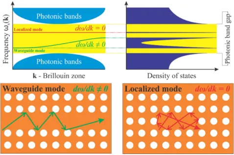
Figure3: Typical dispersion relations of cavity modes, red band, and waveg-uide modes, green band. the corresponding density of states is sketched at right. At bottom, waveguide and localized modes are represented in a two dimensional photonic crystal, where orange and white correspond to different refractive indices.
Photonic crystals become very interesting where “impurities”, known as defects, are introduced in the dielectric lattice. In the same manner as for solid state crystals, where localized states appear due to the im-purities, the electromagnetic field can be localized around dielectric defects, creating allowed states inside the photonic band gap. Defects on photonic crystals can be produced either modifying the geome-try or changing the dielectric properties at specific regions of the lat-tice; in particular, point and linear defects represent the fundamental blocks for the vast majority of systems currently studied. The former is commonly called cavity and the latter waveguide.
Figure 3 shows a schematic representation of the typical bands, in red and green colors, associated to cavity and waveguide modes, re-spectively; the yellow region corresponds to the photonic gap of the system and lighter-blue regions represent the photonic bands. The group velocity dω/dk of cavity modes is zero in all points of the Brillouin zone, while for waveguide modes is in general different from zero. The corresponding photonic density of states is sketched at right in darker-blue; localized modes have the largest density of states, as well as the band edges of waveguide modes and photonic bands edges, where the group velocity is near to zero1. At bottom
of Fig. 3, waveguide and localized modes are represented in a two dimensional photonic crystal, where orange and white correspond to
open the possibility of cavity quantum electrodynamics phenomena, as Purcell enhancement [40] and strong coupling, when light emit-ters are positioned within the photonic crystal nanocavities to interact with the electromagnetic fields [12,19].
2.1.2 Photonic crystal molecules
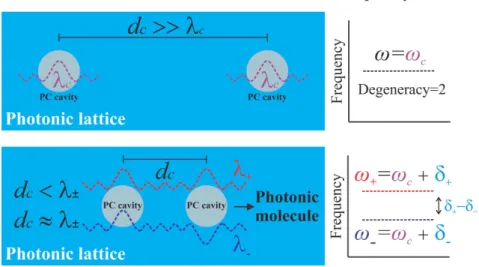
Two or more coupled photonic crystal cavities form a photonic crystal molecule. In Fig. 4 we schematically represent the weak and strong coupling regime of a photonic crystal molecule formed by two iden-tical cavities, which is known as a photonic crystal dimer. When the distance between the two cavities is much larger than their mode wavelengths, i.e., dc >> λc, the spectrum of the system is
degener-ated with the same single cavity frequencies. Over these conditions the system is in the weak coupling regime, and it does not strictly represent a photonic molecule. For intercavity distances smaller than, or of the same order ofλc, the system is in the strong coupling regime
with non-degenerated frequency spectrum determined by the splitted states of the single cavities. In the case of photonic dimers (identical cavities), where the system has a symmetry point, the normal mode frequencies are separated in bonding (subscript +) and antibonding (subscript −) states, resembling atomic molecules. The bonding and antibonding behavior are determined by the symmetry of the electro-magnetic modes; the former is symmetric while the latter is antisym-metric with respect to the symmetry point, as it is shown schemati-cally in Fig. 4, where the symmetry point is at the center of the pho-tonic lattice. The phopho-tonic normal mode frequencies of the molecule can be written as the single cavity frequency plus a coupling termδ, which depends on the amount of overlapping and interference con-ditions between the single cavity modes. In general, the strength of
2 The photonic band gap confinement mechanism for light, based on interference phe-nomena, is known as distributed Bragg reflection (DBR mechanism).
3 The quality factor of a photonic mode measures the photon lifetime within the cavity and it is defined as the ratio between the resonant frequency and the linewidth: Q= δωω.
4 The modal volume of a dielectric cavity measures the effective space occupied by the
photonic mode, and it is defined as:V = R
ǫ(r)|E(r)|2
dr
Figure4: Schematic representation of a photonic crystal molecule formed by two identical cavities, i.e., a photonic crystal dimer, in the weak (above) and strong (below) coupling regimes. The frequency levels for both cases are sketched, correspondingly, at right.
the coupling term δ, which can be positive or negative, is different for bonding and antibonding modes, i.e.|δ+|6=|δ−|, furthermore,
dis-tinct from the atomic case, antibonding ground sates and increasing splitting with increasingdcare possible in photonic crystal molecules
[41].
The delocalized nature of normal modes in photonic crystal molecules will be useful to radiatively couple two semiconductor quantum light emitters in Sec. 3.2, separated by a distance that can be larger than the characteristic wavelength of the system.
2.1.3 Two-dimensional photonic crystal slabs
Figure5: Representation of the total internal reflection and the distributed Bragg reflection mechanisms in two-dimensional photonic crystal slabs.
crystal slabs with high-nanometric precision [4, 5]. Although exper-imental and theoretical complete photonic band gap has not been achieved in these structures up to now, three-dimensional confine-ment is possible for specific mode polarizations as it will be discussed below.
Figure 5shows a typical photonic crystal slab where the two dimen-sional periodic pattern is defined by a square lattice of circular holes in a dielectric planar waveguide. Vertical confinement of light is con-trolled by total internal reflection (TIR)5, and in-plane propagation is
controlled by the photonic pattern via distributed Bragg reflection (DBR); photonic band gaps in these systems are thus conditioned by both TIR and DBR mechanisms. The electromagnetic modes of fully two-dimensional photonic crystals, which are periodic in a cer-tain plane and uniform along the axis perpendicular to that plane, are separated in two orthogonal polarizations, namely, transverse-electric (TE) and transverse-magnetic (TM); considering xy as the plane where the photonic pattern is present, the former has the non-vanishing field components (Ex,Ey,Hz) and the latter has the
non-vanishing field components(Hx,Hy,Ez). The separation of modes in
two different solutions is due to the existence of a symmetry plane parallel to the periodic pattern at any position of the perpendicular axis. Figure 6 schematically shows the two mode polarizations with different symmetry properties for two-dimensional crystals (top). The system is uniform along thezdirection, i.e. thicknessd→∞, and any
plane perpendicular to thezaxis corresponds to a symmetry plane of the system; they are shown three of them in the figure (top), z= ±δ andz=0, where delta is any real number. The electric and magnetic fields are confined at these planes for TE and TM modes, respectively. In comparison with quantum mechanics, where the presence of sym-metry plane on the quantum potential separates the wavefunction
Figure6: Schematic representation of the electromagnetic modes for fully two-dimensional photonic crystals (top), and two-dimensional photonic crystal slabs (bottom). The former has an infinite set of symmetry planes along thezaxis, and the latter has only one sym-metry plane atz=0, i.e., center of the slab.
Figure7: (a) Radiative and guided mode regions on the dispersion rela-tion of a photonic crystal slab; the light line and a quasi-guided mode are illustrated. (b) Band diagram of a typical GaAs two-dimensional photonic crystal slab in the irreducible Brillouin zone.
Photonic band gaps for either TE-like or TM-like modes have been successfully demonstrated through theoretical and experimental stud-ies [47,48,49,50]. The fine-thickness condition along the vertical axis introduces new physical phenomena which are not present in the fully two-dimensional case. Since the space is open outside the pho-tonic crystal slabs, the electromagnetic field is not bounded in this region and it determines a continuous spectrum. On the other hand, the electromagnetic field is bounded inside the slab and the spec-trum is discrete. Discrete resonances, i.e., guided modes, can thus in-teract with the continuous spectrum, i.e., radiative (or leaky) modes, through the vertical boundary, allowing the possibility of energy flux from within to outside the photonic crystal, and vice versa. Figure7(a) illustrates the radiative and guided mode zones in the band diagram of photonic crystal slabs. These regions are separated by the light line, which is defined as the dispersion relation of light in the outside medium; since we are interested in suspended membranes the fron-tier is defined by the dispersion relation of light in air 6, i.e., ω=ck.
Photonic resonances crossing the light line are called quasi-guided modes, and they are subject to out-of-plane diffraction losses, i.e., diffraction processes out of the waveguide plane for the Bloch waves propagating in the photonic crystal slab. In the radiative region of the band diagram, quasi-guided modes are discrete states within a con-tinuum of states, which gives rise to Fano interference phenomena7
[51, 52]. Panel (b) of Fig 7 shows a numerical calculation in
dimen-6 For a general asymmetric two-dimensional photonic crystal slab, where there is a substrate of refractive indexn1and the outside medium has a refractive indexn3,
the light lines areω=ck/n1andω=ck/n3, and the frontier between the radiative
and guided modes is determined by the light line with the largest refractive index. 7 Fano resonances are characterized by asymmetric peaks in the response function
sionless frequency units, using the guided mode expansion method (see following section), of a typical GaAs two-dimensional photonic crystal slab along the edges of the irreducible Brillouin zone. The crystal is formed by a hexagonal lattice of circular holes, with lattice parameter a = 260nm and hole radius r = 65 nm, embedded in a slab of thicknessd=120nm and refractive indexn=3.41. This pho-tonic crystal has a TE-like bang gap, highlighted in yellow, between 0.267 and 0.318, or between 1.274 eV and 1.517 eV in electron-volt units, however, forbidden odd states are not favored by the system and TM-like band gaps are not present. The bands below, fully-above and crossing the light line, correspond to guided, radiative (or leaky) and quasi-guided modes of the slab, respectively.
2.1.4 The guided mode expansion method (GME)
Over the last decade, several numerical methods have been proposed for studying photonic crystal slabs by solving the three-dimensional set of Maxwell’s equations, which in general requires a huge numer-ical and computational effort. Some examples are the plane wave expansion with perfectly matched layers [53], the scattering matrix method [54] and the canonical finite-difference time-domain method (FDTD) [55], the latter has proved to be very flexible for solving the fields in any electromagnetic system, but computationally expensive [56]. Currently, the guided mode expansion method (GME) is the most efficient and reliable approach for solving the photonic disper-sion and radiation losses of photonic crystal slabs, providing numer-ical and computational facilities due, mainly, to the analyticity of the matrix representation of Maxwell operator ˆΘ. Since the GME method is the photonic-crystal-solver used in the present work, the key as-pects of the method will be discussed in this section. For specific de-tails the reader is referred to the original works cited in Refs. [48,57].
2.1.4.1 Photonic dispersion
Starting from the wave equation of Eq. (4) with the corresponding transversality condition in Eq. (6), the magnetic field can be expanded in a set of basis as
H(r) =X µ
cµHµ(r), (12)
subject to the orthonormality condition
Z
H∗µ(r)·Hν(r)dr=δµν. (13)
Equation (4) is then transformed into a linear eigenvalue problem
X
ν
Hµνcν=
ω2
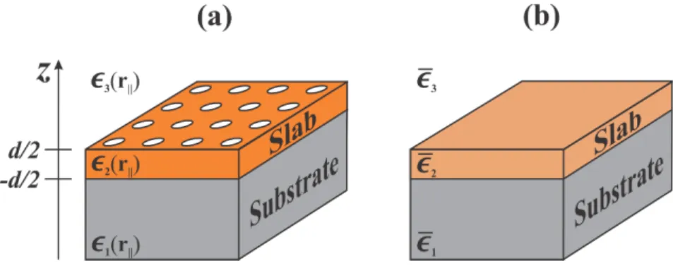
ered between two semi-infinite layers with dielectric functionsǫ1(r||) and ǫ3(r||), namely, the substrate and external media. The basis for expanding the system is defined by the homogeneous planar waveg-uide problem, shown in panel (b), with dielectric constants ¯ǫ1 (lower
cladding), ¯ǫ2 (core) and ¯ǫ3 (upper cladding ) determined by the
aver-ages ofǫi(r||)
¯ ǫi=
1 A
Z
cell
ǫi(r||)dr||, (16)
where the integral is over a unit cell of area A. In order to guided modes be supported by the effective slab, the condition ¯ǫ2 > ǫ¯1, ¯ǫ3
must be fulfilled. Denoting byg=ggˆ the two-dimensional wave vec-tor in thexyplane, and byωgthe frequency of a guided mode which
satisfiescg/√ǫ¯2 < ωg < cg/max(√ǫ¯1,√ǫ¯3)we define the following
quantities:
χ1 = g2−ǫ¯1
ω2g
c2
!1/2
,
qg = ǫ¯2
ω2 g
c2 −g 2
!1/2
,
χ3 = g2−ǫ¯3
ω2g
c2
!1/2
, (17)
representing the real (imaginary) parts of the wave vector in the core (upper and lower cladding), respectively.
By applying Maxwell’s equations to the waveguide problem, transverse-electric (transverse-electric field lying in the xyplane) and transverse-magnetic (magnetic field lying in the plane xy) solutions are determined, re-spectively, by the following implicit equations:
q(χ1+χ3)cos(qd) + (χ1χ3−q2)sin(qd) =0, (18)
q ¯ ǫ2 χ1 ¯ ǫ1
+ χ3
¯ ǫ3
cos(qd) +
χ1χ3
¯ ǫ1ǫ¯3
−q 2 ¯ ǫ2 2
sin(qd) =0, (19)
Figure8: (a) Schematic picture of the photonic crystal slab, where r||
rep-resents the in-plane coordinate vector. (b) Effective homogeneous problem for computing the guided mode basis where ¯ǫ1, ¯ǫ2 and
¯
ǫ3 are the dielectric constants of the lower cladding, core and up-per cladding, respectively.
waveguide interfaces, and the dispersion relationω(g)of the waveg-uide is computed by solving these equations numerically. When sym-metric planar wave guides are considered, i.e. ¯ǫ1 = ǫ¯3 andz = 0 is
a mirror symmetry plane, Eqs. (18) and (19) split into the following equations for odd and even solutions:
qsin
qd 2
−χ1cos
qd
2
=0, TE, even, (20)
qcos
qd 2
+χ1sin
qd
2
=0, TE, odd, (21)
q ¯ ǫ2 cos
qd
2
+ χ1
¯ ǫ1 sin
qd
2
=0, TM, even, (22)
q ¯ ǫ2 sin
qd
2
− χ1
¯ ǫ1 cos
qd
2
=0, TM. odd (23)
The even and odd modes can hence be solved separately reducing the computational effort required by solving directly Eqs. (18) and (19). The solutions of the implicit equations Eqs. (20) to (23) are shown in Fig.9, for the effective homogeneous slab associated to the system of Fig.7(b), i.e., ¯ǫ1=ǫ¯3 =1, ¯ǫ2 =9.218andd=120nm. Irrespective of
the parity of the solutions, TE and TM bands alternate on the condi-tion that the fundamental mode corresponds to a TE polarizacondi-tion. On the other hand, the parity alternates between even and odd solutions for TE and TM polarizations providing that the TE and TM funda-mental modes have even and odd polarizations, respectively. Figure9
shows that the wave vector gcan take, in principle, any value in the xyplane for guided modes8. In the case of two-dimensional photonic
crystal slabs, the modes have the Bloch form shown in Eq. (10), and the k vector is restricted to the first Brillouin zone; larger vectors in
Figure9: Dispersion relation of a symmetric planar waveguide with ¯ǫ1 = ¯
ǫ3=1, ¯ǫ2=9.218andd=120nm.
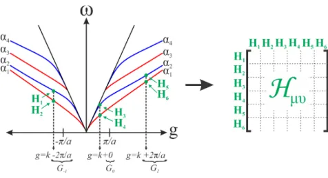
the reciprocal space are generated by adding to k the appropriate reciprocal lattice vector G. Thus, when the photonic crystal is taken into account, the wave vector g can be written in terms of two con-tributions, the Bloch vector kand the reciprocal lattice vector G, i.e., g = k+G. The main effect of the periodic dielectric modulation on the guided bands of the homogeneous waveguide is to fold them to the first Brillouin zone, giving rise to photonic allowed and forbid-den states. Denoting with αtheα-th guided mode, the expansion of Eq. (12) is written for the guided mode basis as
H(r) =X
G,α
c(k+G)Hguidedk+G (r), (24)
where the sum is over the guided modes and reciprocal lattice vectors. The basis set must be truncated in order to obtain a finite number of linear equations determined by Eq. (14). The set of guided modes is truncated up to theα-th element, while the set of reciprocal vectors is truncated providing the cutoff condition|G| <= Gmax, whereGmax
is the maximum vector magnitude considered in the expansion9. To
calculate the matrix elements in Eq. (15), the inverses of the dielectric functions are then expanded in a set of plane waves over the recipro-cal lattice vectors
ǫi(r||)−1 =
X
G
ηi(G)e−iG·r||, (25)
9 This cutoff condition defines a circle centered at the origin of the reciprocal space with radiusGmax, where only reciprocal lattice points inside the circle, with vector
with Fourier coefficients
ηi(G) =
1 A
Z
cell
ǫi(r||)−1eiG·r||dr||, (26) where the integral extends over a unit cell of areaA. The GME matrix elements Hµν are analytical and depend on the matrix elements of
ˆ
ηi, defined as ηi(G,G′) = ηi(G′−G) [48]. A convenient approach
for calculating the elementsηi(G,G′)is based on the Fourier inverse
rule or Ho-Chan-Soukoulis (HCS) method [42], where ηi(G,G′) are
computed by numerical inversion of the dielectric matrix ˆǫi, i.e., ˆηi=
ˆ
ǫ−1i , with Fourier elements ǫi(G,G′) =
1 A
Z
cell
ǫi(r||)ei(G ′−G)·r
||dr
||, (27) This rule has shown to improve the convergence of numerical Fourier-based methods for truncated Fourier representation of discontinuous functions [58].
When the photonic structure has a center of inversion (symmetry point), the matrix elementsηi(G,G′) andHµν are real, then, Eq. (14)
becomes a symmetric eigenvalue problem. In the most general case, where the photonic structures do not have a symmetry point, these matrix elements are complex and Eq. (14) determines a Hermitian eigenvalue problem. This is an important consideration because the computational effort for solving real eigenvalue problems is much lower than for solving the Hermitian ones. The construction of the matrix Hµν is illustrated in Fig. 10 for a one-dimensional slab
pho-tonic crystal with lattice parameter a. We consider Nα = 2 guided
modes and NG = 3 plane waves. For each element of the basis µ,
given a vector k, we associate a guided mode index α and a recip-rocal lattice vector G (plane wave element); the indexµ is therefore univocally represented by k, α and G, i.e., µ = (k+G,α). As it is
shown in the figure, three plane waves and two guided modes deter-mine six orthonormal basis elementsHµ for constructing the matrix Hµν. Hence, the dimension of the eigenvalue problem for computing the photonic dispersion isNα×NG.
Figure10: Schematic representation of the construction of the guided mode basis for calculating the matrix elements Hµν in a one-dimensional photonic crystal slab of lattice parametera. For the sake of simplicity we consider only two guided modes and three plane waves.
2.1.4.2 Radiation losses
The periodic dielectric modulation of the photonic crystal slab folds the guided modes of the effective homogeneous waveguide, lying be-low the light line, to the first Brillouin zone of the photonic lattice. Therefore, photonic crystal resonances can fall above the light line allowing the coupling to radiative modes, i.e., they are subject to in-trinsic losses due to scattering out of the plane. These radiation losses can be estimated through time-dependent perturbation theory using a formulation totally analogous to the Fermi’s golden rule in quan-tum mechanics. The decay rate of a photonic crystal mode |Hphi to
a continuum set of radiative modes |Hradi, at a given frequency ω,
can be represented by
Γph→rad ∝ X
rad
hHph|Oˆp|Hradi
2
ρ(ω), (28)
where ρ(ω) is the photonic density of radiative modes. Since the ra-diation losses are caused by the in-plane periodicity and the vertical boundary condition of the dielectric function, the perturbation opera-tor is represent by ˆOp→ǫ(r)−1. From Eq. (28), the following
expres-sion is obtained for the imaginary part of ω2k/c2 at a givenk in the first Brillouin zone [48,59]:
Im
ω2k c2
= −πX
G′
X
λ=T E,T M X
j=1,3
|Hk,rad|2ρj
k+G′,ω
2 k
c2
Figure11: Representation of the scattering processes with outgoing compo-nents in lower (a) and upper (b) claddings.
where the matrix element between a photonic crystal mode and a leaky mode is
Hk,rad = Z
1
ǫ(r)(∇ ×H
∗
k(r))· ∇ ×Hradk+G′,λ,j(r)
dr. (30)
Equation (29) is known as thephotonic golden rule. Since the field pro-file of a scattering state tends to a plane wave form in the far field, irrespective of the field profile of the photonic crystal slab modes, the mean approximation of the method is introduced by considering the radiative modes of the effective waveguide in the matrix elements of Eq. (30), and the following one-dimensional photonic density of states at a fixed in-plane wave vectorg
ρj
g′,ω
2 c2 = Z∞ 0 dkz 2π δ ω2 c2 −
g2+k2z
¯ ǫj
= ǫ¯ 1/2 j c
4π
θω2−c2ǫ¯g2
j
1/2
ω2−c2g2
¯
ǫj
1/2 , (31)
which is valid for homogeneous planar waveguides. In Eq. (31)δand θare the Dirac delta and Heaviside functions, respectively. All lattice vectors G′, polarizationsλ and scattering processesj = 1 andj = 3 contribute to radiation losses. Such scattering processes, to be con-sidered in the sum of Eq. 29, are illustrated in Fig.11. The outgoing (radiative) components in the lower and upper claddings, which con-tribute to the diffraction losses, are represented by the red arrows in panels (a) and (b), respectively.
Using the expansion of Hk shown in Eq. (24) over the set of guided
modes, the matrix elements of Eq. (30) can be written as
Hk,rad =X
G,α
Qk=
ωk
2Im(ωk), (
34)
where Im(ωk) =Im(ω2k)/[2Re(ωk)].
2.2 semiconductor quantum dots
The confinement of electrons in one, two and three dimensions in nano-structured semiconductors has been the focus of intense research during the last decades for applications on opto-electronic devices [60]. In particular, semiconductor quantum dots, in which electrons are subject to a three dimensional confinement, are characterized by their discrete spectra, long coherence time and large oscillator strengths [9]. These characteristics make them almost ideal artificial atoms that can be fixed in position and integrated into other semicon-ductor structures as photonic crystals, enabling new opportunities for on-chip quantum optics. In fact, quantum dots are promising candi-dates to realize solid state quantum bits (qubits) to be employed in quantum information and communication technologies [6,7,22].
InAs/GaAs/AlAs III-V semiconductor quantum dots, relevant for the present work, are fabricated by epitaxial methods such as molecu-lar beam epitaxy, where the semiconductor heterostructure is grown layer by layer under high-vacuum conditions. The most common ap-proach for generating InGaAs quantum dots is the Stranski-Krastanov method, where a thin wetting layer of InAs is deposited on GaAs; the difference between the InAs and GaAs lattice parameters (7%) generates a strain which is relaxed by the nucleation of randomly positioned islands, i.e., self-assembled quantum dots. They are subse-quently covered by a GaAs layer with the aim of protecting them from surface states and oxidation [8]. Since the InGaAs gap is smaller than the GaAs one, the quantum dot determines three-dimensional con-finement potentials in the valence and conduction bands, for holes and electrons, respectively. Figure 12 illustrates schematically such phenomena, where a InGaAs region is surrounded by GaAs.
Figure12: Schematic representation of a InGaAs quantum dot. The confine-ment potential is created by the different GaAs/InGaAs semicon-ductor band gaps.
dots is obtained. The results shown in the following were taken from the work cited in Ref. [23].
2.2.1 Single-particle and exciton states
The starting point for studying semiconductor quantum dots is the stationary single-particle Schrödinger equation, which can be written in the effective mass and envelope function approximations as
Hi(r)φi(r) =
−h 2
2 ∇ 1
m∗i∇+Vi(r)
φi(r) =Eiφi(r), (35)
where i = e,h denotes electrons or holes, m∗i is the effective mass of the particle i andVi(r) is the three dimensional dot confinement
potential due to the difference between the semiconductor gaps in the heterostructure, see Fig. 12. In Eq. (35) φi(r) is the envelope part of
the total wavefunction
ψi(r) =φi(r)Ui(r), (36)
which describes the slowly varying contribution to the wavefunction over the dot region, andUi(r) is a rapidly varying periodic function
with the period of the crystal lattice [61]. One of the most basic mod-els for Vi(r), providing analytical expressions forφi(r)andEi, is the
harmonic oscillator potential
V(x,y,z) = 1
2m
∗ω2
xx2+
1 2m
∗ω2
yy2+
1 2m
∗ω2
n!2 dx π dx
Here, n labels the quantum state with energy En = (n+1/2)hωx, Hn′s are the Hermite polynomials and dx = [h/(m∗ωx)]1/2. The
ground-sate solution for electrons and holes is then given by the en-velope function
φi(x,y,z) =
1 dxdydzπ3/2
1/2
e− x2 2d2xe
− y2
2d2ye− z2
2d2z, (40)
with energyE0 = 12h(ωx+ωy+ωz).
When an electron is excited with enough energy to be promoted from the valence to the conduction bands, the total charge in the valence band is unbalanced diminishing in one unit the amount of negative charge, which determines an effective positive charge, i.e., a hole. Holes and electrons may form bound states through Coulomb inter-action, in the same manner as protons and electrons in atoms. The bound states of electron-hole pairs in these artificial atoms, namely, quantum dots, are known asexcitons, and they are considered in the electron-hole pair Hamiltonian
H=He+Hh−
e2 4πǫ|re−rh|
+Egap, (41)
whereHeandHhare given by Eq. (35),ǫis the background dielectric
constant of the semiconductor and Egap is the quantum dot band gap energy. The Coulomb term Heh = e2/4πǫ|re−rh| produces a
small shift in the energy states for quantum dots whose sizes are smaller than the corresponding bulk exciton radius (∼35nm for InAs and ∼ 13 nm for GaAs); at this regime the Coulomb interaction can be considered as a perturbation and the energy spectrum is mainly determined by the confinement potentials. Then, the Hamiltonian of Eq. (41) can be rewritten as
H=H0+Heh, (42)
and the solutions ofH0, which are the antisymmetric excitonic
wave-functions, can be written in the following form:
Ψ=Aψn′(re,σe),ψm(rh,σh)
whererandσare position (with respect to the center of the dot) and spin variables, respectively, n andm labels the quantum states, and Arepresents overall antisymmetry. The wavefunction of Eq. (43) rep-resents an electronψ′
n(re,σe)which has been promoted from the
va-lence band into a conduction band, while ψm(rh,σh)represents the
hole state created in the valence band. By considering the same poten-tial in all three directions, i.e.,dx=dy=dz =d= [h/(m∗ω)]1/2, the
first order correction to the ground state energy due to the Coulomb interaction is given by [23]
E0,eh=hΨ0|Heh|Ψ0i=
1 2
e2
π3/2h1/2ǫ
s m∗
em∗hωeωh
m∗
eωe+m∗hωh
, (44)
where the exchange interaction term, which is much smaller than the direct one10, is not considered in this calculation.
2.2.2 Förster coupling between two quantum dots
Excitons from different quantum dots can be coupled via Coulomb interaction if the interdot distances are of the order of the dot sizes. In particular, the Förster coupling, which can be under certain con-ditions of dipole-dipole type, is responsible for resonant exciton ex-change, or resonant energy transfer, between the quantum dots. The Förster interactionVFcan be estimated within first order perturbation
theory by
VF =hΨi|HF|Ψfi, (45)
considering the Coulomb Hamiltonian
HF = 1
4πǫ
e2
|R+r1−r2|
, (46)
whereR,r1 andr2 correspond to the interdot separation vector, and
the position vectors defined from the centers of the dot 1 and dot
2, respectively. These vectors are schematically shown in Fig. 13 for two interacting quantum dots. For calculating the matrix element of Eq. (45), the following initial and final states can be considered:
Ψi=A
ψn′(r1,σ1),ψm(r2,σ2)
, (47)
Ψf=A
ψn(r1,σ1),ψm′ (r2,σ2)
.
Here, Ψi represents a conduction band state in dot 1 and a valence
band state in dot 2, andΨf represents a valence band state in dot 1
and a conduction band state in dot 2, i.e, a resonant exciton transfer 10 The exchange interaction term comes from the integrals with arguments of the form ψn′∗(r1)ψm(r1)ψn′(r2)ψ∗m(r2), while the direct interaction term comes from the
inte-grals with arguments of the formψ′∗
Figure13: Schematic illustration of two interacting quantum dots.
from dot 1to dot2mediated by the Coulomb interaction. The direct matrix element of Eq. (45) is then given by
VF = −
e2
4πǫ
Z Z
ψn′∗(r1)ψn(r1)
1
|R+r1−r2|
ψ∗m(r2)ψm′ (r2)dr1dr2. (48)
The Coulomb term in Eq. (48) can be expanded in Taylor series about the vector R up to second order for |R| ≫ |r1−r2|, leading to the
following expression for the Förster interaction energy:
VF = −
e2 4πǫR3
hrIi · hrIIi−
3
R2(hrIi ·R) (hrIIi ·R)
, (49)
where the integrals
hrIi=
Z
ψn′∗(r1)r1ψn(r1)dr1, (50)
hrIIi=
Z
ψm∗ (r2)r2ψm′ (r2)dr2,
are calculated on dot 1 and2, respectively, between an electron (ψ′) and a hole (ψ) states. The behavior of the Förster coupling as a func-tion of Ris clearly seen From Eq. (49); for |R| ≫ |r1−r2| the Förster
energy transfer mechanism displays a R−3 dependence. This short-range interaction is a great limitation for independent manipulation of the quantum dots when they are strongly coupled, which is crucial for quantum information applications. In view of solving such limi-tation, the present work explores the possibility of using photonic modes for long-range dot-dot interaction beyond the Förster regime.
2.3 semiconductor quantum dots in photonic crystals
all localized qubits. For solid state qubits, i.e., quantum dots, the pho-tons are the best candidates to achieve such a quantum bus platform, due to their long coherence time and high velocity. In view of this, there is a growing theoretical and experimental interest to control the photon-mediated interaction (radiative coupling) between two quan-tum dots through the electromagnetic modes in a semiconductor pho-tonic crystal structure [24,25,62]. Due to their exceptional capabilities to efficiently guide and confine the electromagnetic radiation, and the high degree of precision in fabrication techniques currently achieved, photonic crystals should allow to overcome the short-range Förster coupling between interacting quantum dots, thus achieving sizable effective radiative interaction at distances quite larger than their emis-sion wavelength [29].
The radiative coupling between quantum dots is discussed in this sec-tion within a semiclassical formalism. Furthermore, a fully quantum mechanical formulation of the problem is presented for quantifying the amount of entanglement between quantum dots, which are cou-pled via photon-mediated interactions.
2.3.1 Semiclassical formalism
A useful semiclassical formalism was described by Minkov and Savona in Reference [26] to studyNquantum dots coupled toM electromag-netic photonic modes in an arbitrary dielectric structure. Following this work, our starting point is the inhomogeneous wave equation for the electric field [see Eq. (5)] with a polarization vector source, which can be written in Gaussian units as follows:
∇ × ∇ ×E(r,ω) −ω 2
c2 [ǫ(r)E(r,ω) +4πP(r,ω)] =0. (51)
The underlying photonic structure is considered through the spatial dependence of the dielectric function ǫ(r), while the linear optical response of the quantum dots is included through a nonlocal suscep-tibility tensor in the polarization vector
P(r,ω) = Z
ˆ
χ(r,r′,ω)E(r,ω)dr′. (52)
We will consider the specific case of excitons originating from the heavy-hole band of a semiconductor with cubic symmetry (e.g. InAs). In this case the x and y components of the polarization couple to the electromagnetic field according to the following susceptibility tensor[63,64]:
ˆ
χ(r,r′,ω) = µ 2 cv h N X α=1 Ψ∗
α(r)Ψα(r′)
ω(α)−ω
1 0 0 0 1 0 0 0 0
treatment all the frequencies are assumed to be complex quantities, i.e., ω(α) = Re{ω(α)}−iγ(α)/2 and ωm = Re{ωm}−iγm/2, where
γ(α)represents the overall decay rate of the exciton state associated to the quantum dot α, and γm represents intrinsic and extrinsic losses
of the photonic modem.
Introducing the quantities Q(r,ω) = pǫ(r)E(r,ω), the wave
equa-tion Eq. (51) is turned into a self-adjoint inhomogeneous differential equation [3]:
ΥQ(r,ω) −ω 2
c2 Q(r,ω) =
4π p
ǫ(r)
ω2 c2
Z
ˆ
χ(r,r′,ω)Q(r
′,ω) p
ǫ(r′) dr ′, (55)
with associated self-adjoint differential operator
Υ= p1
ǫ(r)∇ × ∇ ×
1 p
ǫ(r). (56)
Since the susceptibility tensor in Eq. (53) decouples the z-polarized fields, we define the two-dimensional fieldQ= (Qx,Qy), and we can
express the formal solution of the inhomogeneous problem of Eq. (55) using the Green’s function approach:
Q(r,ω) =Q0(r,ω)+
4π p
ǫ(r)
ω2 c2
Z
dr′ Z
dr′′Gˆ(r,r′,ω)χˆ(r
′,r′′,ω) p
ǫ(r′′) Q(r ′′,ω).
(57) The Green’s tensor can be expanded onto the set of the orthonormal eigenfunctions of the self-adjoint operator of Eq. (56):
ˆ
G(r,r′,ω) =X m
Qm(r)⊗Q∗m(r′) ω2
m
c2 −
ω2
c2
, (58)
where the outer product is defined as
A⊗B= AxBx AxBy
AyBx AyBy
!
In the vast majority of structures, the quantum dots are embedded within a semiconductor dielectric medium of dielectric constant ǫ∞, i.e., the wave functions are non-negligible only in the region where ǫ(r) = ǫ∞. Thus, we can safely substitute pǫ(r′) = pǫ(r′′) = ǫ
∞
in Eq. (57), since the r dependence of all quantities will be consid-ered into the overlap integrals with the quantum dot wavefunctions. Furthermore, a very good approximation consists in replacing the ω on the right side of Eq. (57), as well as (ωm+ω)/2, obtained from
the factorization of the denominator in Eq. (58), with an average ex-citon transition frequency,ω0. The resonances of the coupled system
are computed considering the homogeneous problem associated to Eq. (57) (withoutQ0(r,ω)), which determines the particular solution
of Eq. (55). Then, defining
Qα(ω) = Z
ΨαQ(r,ω)dr, (60)
we obtain
Q(r,ω) = 2πω0
ǫ∞ µ2cv
h N X α=1 M X m=1
Qm(r)⊗Qαm∗ (ωm−ω)(ω(α)−ω)
Qα(ω). (61)
Integrating Eq. (61) withRdrΨβ(r)and definingQe(ω) =Qα(ω)/(ω(α)−
ω), the following set of equations are obtained for the complex fre-quency poles:
(ω(β)−ω)Qeβ(ω) = 2πω0
ǫ∞ µ2 cv h N X α=1 M X m=1
Qβm⊗Qαm∗ (ωm−ω)
e
Qα(ω). (62)
It is easy to show that the nonlinear system of Eq. (62) is mathemati-cally equivalent to diagonalize the matrix [26]
Λ=
ω(1)x 0 · · · 0 g11,x · · · g1M,x
0 ω(1)y · · · 0 g11,y · · · g1M,y
..
. · · · . .. ... ... · · · ...
0 0 · · · ω(N)y g1N,y · · · gNM,y
g11∗,x g11∗,y · · · gN1,y∗ ω1 · · · 0
..
. · · · . .. ... ... · · · ...
g1M∗,x g1M∗,y · · · gNM∗,y 0 · · · ωM
part) and loss rates (−2×imaginary part) of the mixed excitations of the system, known aspolaritons, and their corresponding eigenvectors
λ= λ1x,λ1y,. . .,λNx,λNy,λ1,. . .,λM, (65)
define the Hopfield coefficients, whose square moduli are interpreted as the bare-exciton (or bare-photon) fractions of the polariton state [65,66].
For typical self-organized InGaAs quantum dots, whose size lies in the10-20nm range and the exciton recombination energy is∼1.3eV (λ ≈ 950 nm), a point dipole assumption, Ψα(r) = Cδ(r−rα), is a
very good approximation because the electric field varies weakly in a region where Ψα(r) is non-negligible. Since the wave function is
not properly normalized at equal electron and hole positions, the constant C, which depends on the oscillator strength, can be esti-mated through experimental measurements of the quantum dot ra-diative decay rate. Following Minkov and Savona [26], and Parascan-dolo and Savona [67], with a radiative lifetime of 1 ns and excita-tion energy hω0 ≈ 1.3 eV, the square dipole moment is found to be
d2 ≈0.51eV nm3, which is related toCthrough the expression:
d2 =µ2cvC2. (66)
Within the point dipole approximation, the coupling constants of Eq. (64) are turned into the simple following form:
gαm = gαm,x,gαm,y
=
2πω0
ǫ∞h
1/2
dQm(rα). (67)
From Eq. (62) we define the following tensor [33]:
ˆ
Gαβ(ω) = M X
m=1
gβm⊗gαm∗ (ωm−ω)
=d2 2π ǫ∞h
ω2
c2 Gˆ(rα,rβ,ω), (68)
where ˆG(rα,rβ,ω)is the Green’s tensor evaluated at the quantum dot
positions rα and rβ. The components Gαβxx, Gαβxy, Gαβyx and Gαβyy are
dotαand dotβat the excitonic transition frequencyω.
Finally, the last requirement of the model are the values of the nor-malized photonic eigenmodesQmat the quantum dot positions, and
their corresponding eigenfrequencies and loss rates, which are com-puted using standard methods to solve photonic crystal structures. Since we are interested in studying the radiative interaction between quantum dots in photonic crystal slabs molecules, we employ the guided mode expansion approach for this task, which is the best compromise between computational effort and reliable results for ex-tended and strong localized modes in high dielectric regions.
2.3.2 Quantum formalism
The quantum theory of electromagnetic fields commonly adopted in quantum optics books, and their corresponding interaction with lo-calized quantum emitters, does not consider the spatial dependence of the dielectric permittivity [68, 69]. Some of these approaches are even restricted to vacuum only. The rigorous formulation of the fully quantum radiation-matter interaction problem in spatially dependent dielectric materials is lengthy and not trivial, and it has been ad-dressed in Refs. [70,71], where the so calledmultipolar Hamiltonian11
is formally deduced. The details of this field quantization are not pre-sented here and the reader is referred to the original works.
We start from the second-quantized multipolar Hamiltonian for the case of neutral, stationary radiative quantum emitters in a neutral, nonconducting, dielectric medium in the dipole and rotating wave approximations12:
ˆ H0 =
X
n
hωnaˆ†naˆn+ X
α
hω(α)bˆ†αbˆα
+hX
nα
g∗nαaˆ†nbˆα+gαnaˆnbˆ†α
, (69)
whereωnandω(α)denote the frequency of the photonic modenand
the excitonic transition frequency of the quantum dotα, respectively;
11 All the multipolar contributions are considered in the field-matter coupling. 12 When the wavefunction of the quantum emitters varies vary rapidly in relation to the
electric field, a very good approximation is to consider a dipole radiation-matter cou-pling, i.e., the quantum emitter does not feel electric field variations and the value of the field amplitude is approximately constant in the region where the wavefunction is non-negligible. This is the so calleddipole approximation. Moreover, when we are interested in the resonant regime of the system, terms with very high frequency in the radiation-matter coupling can be safely neglected. These rapidly rotating terms usually have the forms ˆa†nbˆ†αand ˆanbˆα. This is the so calledrotating wave
ˆ
bα, ˆbµ =δαµ, (71)
and all other anticommutators vanish. In the present theory, the light-matter coupling strength between the mode nand the quantum dot αis given in Gaussian units as [25]
gαn=
r
2πω(α)
h dα·En(rα), (72)
wheredα =dαeαdenotes the dipole moment of the quantum dotα
with magnitude dα and orientation eα, and En are the eigenmodes
of Eq. (5) subject to the normalization condition
Z
ǫ(r)E∗n(r)·Em(r)dr=δnm. (73)
Equation (72) is totally equivalent to Eq. (67) obtained by semiclassi-cal means. In the present approach, mutual coupling between semi-conductor quantum dots is not considered because we are interested in dot separations which are beyond the Förster and exchange (tun-neling) regimes. However, all photonic modes interact with all quan-tum dots, giving rise to an indirect photon-mediated interaction be-tween them, i.e., to a radiative coupling.
We now consider an exciton coherent pumping in the Hamiltonian of Eq. (69) through the driven term
ˆ
Hp(t) =h X
α
h
Λα(t)e−iωptbˆ†α+Λ∗α(t)eiωptbˆα
i
, (74)
where Λα(t) is the pumping rate at which are coherently created
electron-hole pairs in the quantum dot αby a pump laser or electric potential with frequencyωp. Here, we focus on the continuous wave
excitation regime, in which the pumping rates Λα(t) are time
inde-pendent and can be written in the formΛα(t) =Ωαeiφα, where Ωα
is a real amplitude and φα is a real phase. The total Hamiltonian of
the system is then written as
ˆ
H(t) =Hˆ0+h X
α
h
Ωαe−i(ωpt−φα)bˆ†α+Ω∗αei(ωpt−φα)bˆα
With the purpose of eliminating the explicit temporal dependence of the Hamiltonian in Eq. (75), the system dynamics can be described in a rotating frame of reference with frequency ωp by applying the
operator
ˆ
R(t) =exp "
iωpt X
n
ˆ a†naˆn+
X
α
ˆ b†αbˆα
!#
, (76)
determining an effective Hamiltonian ˆHeff = RˆHˆRˆ†−ihR dˆ Rˆ†/dt
, i.e.,
ˆ Heff =
X
n
hω¯naˆ†naˆn+ X
α
hω¯(α)bˆ†αbˆα
+hX
nα
g∗nαaˆ†nbˆα+gαnaˆnbˆ†α
+hX
α
Ωαeiφαbˆ†α+Ω∗αe−iφαbˆα
,
(77) where ¯ωn=ωn−ωpand ¯ω(α) =ω(α)−ωp.
We adopt the master equation formalism for describing the dissipa-tive dynamics of the system, which is written in Markov approxima-tion for the rotated density matrix, ˜ρ=Rρˆ Rˆ†, as:
dρ˜ dt =
i h
˜ ρ, ˆHeff
+X
m
ˆ
L(γm) + X
α
ˆ
L(γ(α)), (78)
where
ˆ
L(γm) =γm
ˆ
amρ˜aˆ†m−aˆ†maˆmρ/2˜ −ρ˜aˆ†maˆm/2
, (79)
and
ˆ
L(γ(α)) =γ(α)bˆαρ˜bˆ†α−bˆα†bˆαρ/2˜ −ρ˜bˆ†αbˆα/2
, (80)
are the Lindblad operators corresponding to the radiative losses of the photonic modemat a rateγm(intrinsic and extrinsic losses13) and
the losses by spontaneous emission in the quantum dotαat exciton decay rateγ(α). The master equation of Eq. (78) is obtained by consid-ering that the system is coupled to a broadband spectrum and very large (immense number of degrees of freedom) ensemble of harmonic oscillators at thermal equilibrium, known as bath or reservoir, lead-ing to a irreversible damplead-ing and quantum decoherence. The system-reservoir dynamics, ρsr(t), is solved using time-dependent
perturba-tion theory up to second order (the system is assumed to be weakly coupled to the reservoir), and the total density operator is traced over
where γ(m)d represents a pure dephasing rate. Lindblad dissipation terms associated to incoherent pumping could also be considered in the master equation [24], however, since we are interested in low ex-citation, low temperature and resonant excitation regimes, they are safely neglected. Finally, the steady state of the system, ˜ρss is found
by solving the equation
dρ˜
dt =0, (82)
which determines a linear system of algebraic equations that must be inverted to obtain ˜ρss. Such an approach is however computationally
expensive and very inefficient for large Hilbert spaces. In order to avoid numerical inversions, the system of Eq. (82) can be turned into an eigenvalue problem by following the next steps. First, we take advantage of the linearity of master equation and write Eq. (78) in the form
dρ˜
dt =Tˆρ˜, (83)
by constructing the right operators ˆORwhich satisfy the relation
˜
ρOˆ =OˆRρ˜ (84)
where ˆO represents any operator of Eq. (78) on the right side of ˜ρ. Second, considering that Eq. (83) has dimensionN, we define the col-umn vector[ρ˜]with dimensionN2and the matrix [[ ˆT]] with dimension N2×N2 such that
[[ ˆT]][ρ˜] = [Tˆρ˜]. (85)
Third, we define the eigenvalue problem
[[ ˆT]][ρ˜] =λ[ρ˜], (86)
where the steady state solution correspond to the eigenstate with cor-responding eigenvalue λ = 0. Finally, the steady state density ma-trix ˜ρss is constructed from the eigenvector [ρ˜]ss following the rule
2.3.2.1 Two-qubit entanglement
Two quantum mechanical systemsρ1 andρ2 whose total density
op-erator cannot be written in the factorized form
ρT =ρ1⊗ρ2, (87)
are said to be entangled. Entanglement, which is a fully quantum mechanical phenomenon, describes situations where the systems ex-hibit quantum correlations such that we cannot describe one of them without referring to the others. In particular, photon-mediated in-teractions between semiconductor quantum dots allow the possibil-ity of exciton entanglement, and we can take advantage of the non-separability of the whole system state for quantum information trans-ferring between single spatially separated quantum dots. The quan-tification of entanglement is hence fundamental for applications in quantum technologies, but this is a very hard task for many-body systems and it is focus of intense research up to now [72,73,74]. We are nonetheless interested in a two-qubit system using two-level quan-tum dots, for which quanquan-tum entanglement has been widely studied [75, 76, 77, 78]. Here, we adopt the Peres-Horodecki negativity cri-terion, which leads to a sufficient condition for non-separability of composite systems in composite Hilbert spaces of dimension 2⊗2 and 2⊗3 [79, 80, 81]. Since our two-quantum-dot system is inter-acting with a photonic environment, the two-qubit reduced density operator ρQD1QD2 of dimension 2⊗2, is calculated by tracing the
whole density operator, ρ, over all photonic degrees of freedom of the system
ρQD1QD2=Tr(ρ)ph. (88)
The negativity is defined as the absolute value of the sum of the neg-ative eigenvalues ofρT1
QD1QD2, where T1 represents the partial
trans-pose of ρQD1QD2 with respect to the system 1, i.e., quantum dot 1.
For example, consider a system of two quantum dots and one pho-tonic mode, the matrix elements of the density operator in a Fock basis can be written asραµm,α′µ′m′ whereαandµdenote the excita-tion number,0or1, in the two-level quantum dot1and2, respectively, andmdenotes the photon number, which is a positive integer, in the photonic mode of the system. Following Eq. (88), the matrix elements of the quantum dot reduced density operator, which will be denoted byσ, are given by
σαµ,α′µ′ =
X
m
ραµm,α′µ′m, (89)
and the matrix elements of the partial transpose ofσwith respect to the quantum dot1read
σT1
|φ i= √
2(|00i ±|11i) (91)
|ψ±i= √1
2(|01i ±|10i), (92) where the corresponding density operators are given by
ˆ
ρφ± =|φ±ihφ±|, ρˆψ± =|ψ±ihφ±|. (93) Considering the ordering of the basis{|00i,|01i,|10i, |11i}, the matrix representations of the density operators in Eq. (93) read
ρφ± = 1 2
1 0 0 ±1 0 0 0 0 0 0 0 0
±1 0 0 1
, ρψ
± = 1 2
0 0 0 0
0 1 ±1 0 0 ±1 1 0
0 0 0 0
. ( 94)
The matrix elements of ρT1, namely, the partial transpose of ρ with respect to qubit1, i.e., the first entry of|α1α2i, are obtained from the
matrix elements ofρfollowing the rule of Eq. (90)
hα1α2|ρT1|α1′α2′i=hα1′α2|ρ|α1α2′i. (95)
The matrix representations ofρT1
φ± andρ
T1
ψ± are then
ρT1
φ± = 1 2
1 0 0 0
0 0 ±1 0 0 ±1 0 0
0 0 0 1
, ρ
T1 ψ± =
1 2
0 0 0 ±1 0 1 0 0 0 0 1 0
±1 0 0 0 . ( 96)
Finally, it is easy to show that the characteristic equation to find the eigenvalues λof the four matrices in Eq. (96) is
(0.5−λ)3(0.5+λ) =0, (97)