Study of the Nanostructure Efect on Polyalkylthiophene Derivatives Films Using
Impedance Spectroscopy
Lucas Vinicius de Lima Citolinoa, Maria Luisa Braungera, Vinícius Jessé Rodrigues Oliveiraa,
Clarissa A. Olivatia*
Received: September 15, 2016; Revised: January 06, 2017; Accepted: February 18, 2017
In this paper, devices fabricated with a diode-like structure (electrode/polymer/electrode) from spin-coated and nanostructured (Langmuir-Schaefer) ilms of polythiophene derivatives were characterized by impedance spectroscopy and studied by theoretical itting to reach a better understanding of the physical processes in the devices. The materials used for this research were the polyalkylthiophene (P3AT) derivatives poly(3-butylthiophene) (P3BT), poly(3-hexylthiophene) (P3HT), poly(3-octylthiophene) (P3OT) and poly(3-decylthiophene) (P3DT). Electrical measurements were performed from 1 Hz to 1 MHz (100 mV ac) while increasing the dc bias in the range from 0 to 2.5 V. The ittings of the experimental results were performed using equivalent circuits. By plotting the theoretical and experimental spectra on a single graph, it was possible to obtain information related to the ilm morphology, interfacial efects, resistance, capacitance and conductivity of the polymer, thereby enhancing the understanding of this particular type of device. Among the P3AT ilms, those grown by the Langmuir-Schaefer technique showed higher electrical conductivity, with the only exception being that of P3BT.
Keywords: polythiophene, nanostructured ilm, impedance spectroscopy
* e-mail: [email protected]
1. Introduction
Polythiophenes have been a particular focus among conventional conductors due to their good stability and easy processability1,2. In some reports, attention has been paid to regioregular polyalkylthiophene derivatives (P3AT), where the increased alkyl chain length of the polymer increases its solubility, a property that is extremely important for the production of high-quality organic electronic devices2,3. In organic electronics, P3AT thin ilms ofer a number of applications, such as in light-emitting diodes, sensors and solar cells4–9. The thin ilms can be fabricated by deposition techniques such as spin-coating, Langmuir-Blodgett (LB) and Langmuir-Schaefer (LS)10–12.
Impedance spectroscopy analysis has proven to be a useful technique to study the electrical properties of devices built from thin ilms of semiconductor materials13. The technique consists of measuring the complex impedance (Z*) over a wide frequency range (f)12,14. From the spectrum of Z*vs.
f, relevant information can be obtained, such as the bulk conductivity, as well as data on the interface between the electrode and materials, such as the injection and charge accumulation15. One analysis tool is theoretical models based on equivalent circuits that can adequately explain the results obtained from the impedance spectra14–16. This is a simple way to describe the features of structures containing
an active layer between two electrodes, by using elements in the circuit17.
The present study addresses the inluence of the thin ilm deposition technique as applied to P3AT derivatives as measured by impedance spectroscopy. The LS technique provides nanostructured thin ilms, and it was compared herein to the widely used spin-coating technique. The transport mechanisms of the charge carriers were evaluated through impedance spectroscopy results for diferent P3AT derivatives and morphologies. The interfacial electrical features of the devices were analyzed by the theoretical modeling of the experimental results.
2. Materials and Methods
The materials used for this study were the P3AT derivatives poly(3-butylthiophene) (P3BT), poly(3-hexylthiophene) (P3HT), poly(3-octylthiophene) (P3OT) and poly(3-decylthiophene) (P3DT), all obtained from Sigma-Aldrich. Regarding the regioregularity, the values found for the P3BT, P3HT, P3OT and P3DT were approximately 80 – 90%, ≥ 90%, ≥ 90 %, 98.5%, respectively. The polymers were used as thin ilms deposited by the spin-coating and LS techniques onto ITO (indium-tin oxide) substrates (Delta Technology), which has an average covered area of 1.6 cm2 and the sheet resistance (Rs) between 5 and 15 Ω.
The spin-coating technique is used to fabricate thin ilms onto plain substrates. A spinner was used for the
a Faculdade de Ciências e Tecnologia, Universidade Estadual Paulista, CP 467, 19060-900 Presidente
875
Study of the Nanostructure Efect on Polyalkylthiophene Derivatives Films Using Impedance Spectroscopy
production of the thin ilms, with rotation speed of 1000 rpm for 60 seconds. The P3AT derivatives were dissolved in chloroform in solutions of 15 mg/ml, except P3BT which had a concentration of 10 mg/ml due to the diiculty to solubilize this material in large quantities18.
A LS ilm is made of one or more layers of stabilized Langmuir ilm by a horizontal contact of the substrate with the monolayer at constant surface pressure (SP) followed by a slowly lift of the substrate. For the LS ilms, the P3AT derivatives were dissolved also in chloroform, however in solutions with concentration of 0.2 mg/ml. The P3BT derivative was deposited in SP = 30 mN/m, while the derivatives P3HT, P3OT and P3DT were deposited in SP = 20 mN/m18.
The thicknesses of the ilms were determined by a Veeco Dektak 150 proilometer. The thicknesses of the P3AT ilms obtained by proilometry measurements for P3BT, P3HT, P3OT and P3DT were approximately 101, 129, 96 and 133 nm for the spin-coated ilms and 71, 317, 233 and 220 nm for the LS ilms, respectively. The numbers of deposited layers were 10, 25, 25 and 15 for the P3BT, P3HT, P3OT and P3DT ilms, respectively. Aluminum (Al) electrodes were deposited onto the P3AT ilms by physical vapor deposition using an Edwards 306 Auto Evaporation System, forming a diode-like structure of ITO/P3AT/Al.
The electrical measurements were carried out using a Solartron impedance analyzer, mod. 1260A. The amplitude of the ac signal applied was 100 mV, and the frequency (f) ranged from 1 to 106 Hz. A superposed dc bias was applied to the ac signal, from 0 to 2.5 V. The results were analyzed by the impedance spectra: imaginary impedance (-Z”) versus real impedance (Z’), -Z” versus f and Z’ versus f. From the impedance spectra were obtained the parameters for the equivalent electrical circuits used in the theoretical modeling.
The theoretical models were proposed using equivalent electrical circuits of associated resistors and capacitors. The resistors are used to represent the possible resistance of the materials or the interface resistance between two diferent materials. The capacitors, on the other hand, are used to represent the charge accumulation at the interfaces, thus deining the characteristic relaxation times of the studied structures. The theoretical model applied was the equivalent circuit (equation (1))17, in which the α parameter analytically simulates the distribution of the dielectric relaxation time τ, where 0 ≤ α ≤ 1.
The electrical conductivity of the materials was calculated from the equation (2), where l is the ilm thickness (in nm), A is the efective area of the device (in cm²) and R the resistance of the material used (in Ω).
*
( )
Z
R
R C
R
R C
R
R C
R
R C
R
j
1
1
1
1
1
1 11 1
2 21 2
1 11 1
2 21 2 1 2 1 2
~
~
~
~
=
+
+
+
+
+
+
+
+
a a a a - ---T
Q
Q
Q
Q
V
V
V
Y
V
The model provides a symmetric distribution of the relaxation times and facilitates the development of more complex models. Applying Mathcad software version 14.0, the analysis of the experimental data and the theoretical modeling of the electrical measurements were performed.
( )
R
A
l
1
2
$
v
=
3. Results and Discussion
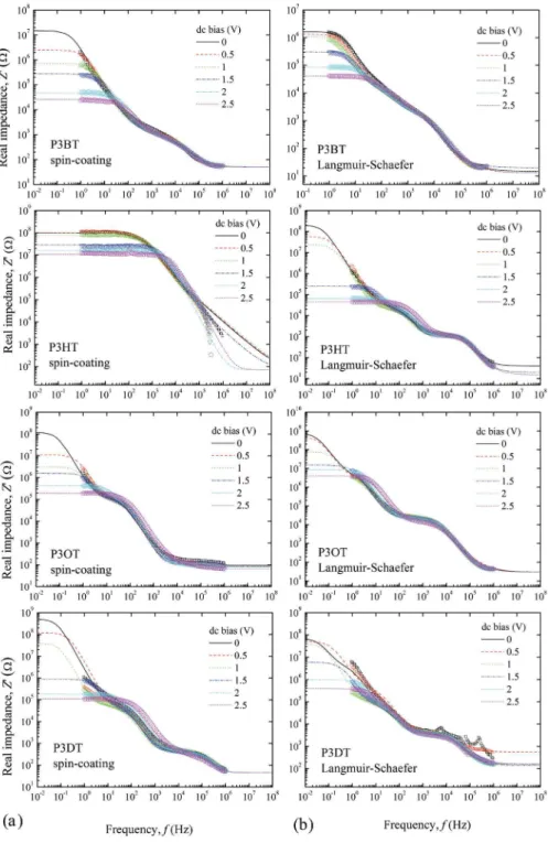
The Z’ vs. f plots obtained for the ITO/P3AT/Al devices, in which the P3AT ilms were deposited by the spin-coating (ITO/P3AT(spin-coating)/Al) and LS (ITO/P3AT(LS)/Al) techniques, are shown in Figure 1. The experimental results are represented by open symbols, while the diferent types of lines are the theoretical ittings. Through these results, one can see some similarities between the spectra of the devices.
In the Z’ vs. f data, there is a behavior where Z’ tends to reach constant values (plateaus) at low and high frequencies. This is a clear result for some plots, as for the P3HT spin-coated ilm at low frequencies, but it is not evident for others, and this justiies the use of theoretical itting. The plateaus shift at low frequencies according to the dc bias applied. This result is possibly related to the reduction of the potential barrier at the Al/P3AT interface when the applied dc bias increases17.
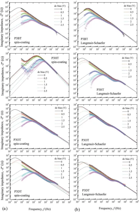
Figure 2 shows the -Z” vs. f plots obtained for ITO/ P3AT/Al devices in which the P3AT ilms were deposited by spin-coating (ITO/P3AT(spin-coating)/Al) and LS (ITO/P3AT(LS)/Al) techniques. As for the Z’ vs. f plots, the experimental results are represented by open symbols, while the diferent types of lines are the theoretical ittings.
In the -Z” vs f spectra, for the spin-coated and LS ilms
of P3BT, there can be observed one well-deined relaxation peak that shifts to lower frequencies with the increase in the dc bias applied. For the P3HT spin-coated ilm, there is only one relaxation peak that shifts in the middle frequencies, while the P3HT LS ilm presents two relaxation peaks, one that shifts from low to medium frequencies (approximately 10 to 102 Hz) and the other, less deined, remains constant at high frequencies. For the spin-coated and LS ilms of P3OT, there is only one well-deined relaxation peak formed, similar to the P3BT case. However, it is possible to observe the formation of a shoulder peak at approximately 104 Hz for the P3OT LS ilm. For the spin-coated and LS ilms of P3DT, there may be observed one well-deined relaxation peak at low frequencies and one shoulder peak at higher frequencies. The shoulder peaks improve their deinition with the applied dc bias.
Figure 1. Z’ vs. f plots for ITO/P3AT/Al devices containing a) spin-coated and b) LS ilms. The experimental
results are represented by open symbols.
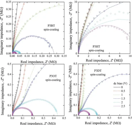
two or more semicircles. In all diagrams, Z* tends to form smaller semicircles upon increasing the dc bias voltage, wherein the diameter of the semicircle is related to the total resistance of the device19. In the theoretical ittings, each circle shall be related to an RC circuit in parallel.
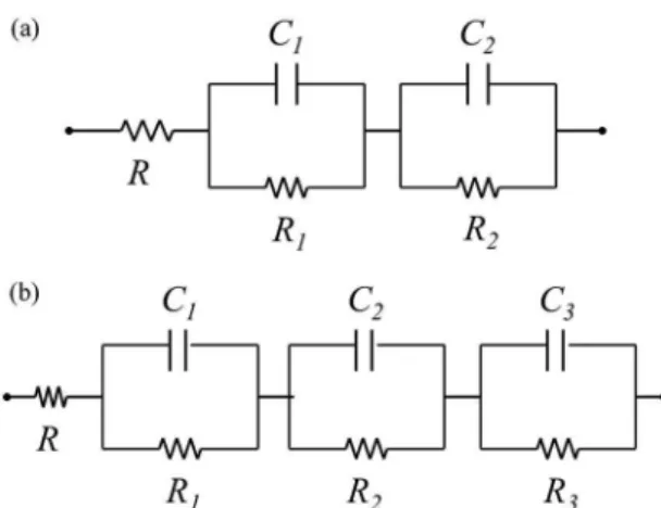
The experimental data were analyzed using the electrical circuits shown in Figure 5. For the devices of the P3AT
877
Study of the Nanostructure Efect on Polyalkylthiophene Derivatives Films Using Impedance Spectroscopy
Figure 2. -Z” vs. f plots for ITO/P3AT/Al devices containing a) spin-coated and b) LS ilms. The experimental
results are represented by open symbols.
parallel RC circuit required in the theoretical itting for the ITO/P3AT(LS)/Al devices.
Through theoretical ittings of the Argand diagrams, for most devices in which the P3AT derivatives were deposited by the spin-coating technique, it is possible to evaluate the superposition of two semicircles. Only for the ITO/ P3DT(spin-coating)/Al device did the theoretical itting show the superposition of three semicircles. As for the
ITO/P3AT(spin-coating)/Al devices, the ITO/P3AT(LS)/Al devicesalso exhibited only one semicircle, but in this case, it was due to the superposition of three semicircles. Table 1 shows the parameters obtained by ittings performed on the experimental curves shown in impedance spectra at a dc bias of 0 V.
Figure 3. Argand diagrams for the ITO/P3AT(spin-coating)/Al devices. The experimental results are represented by open symbols.
Figure 4. Argand diagrams for the ITO/P3AT(LS)/Al devices. The experimental results are
879
Study of the Nanostructure Efect on Polyalkylthiophene Derivatives Films Using Impedance Spectroscopy
Figure 5. Equivalent electrical circuits used in the theoretical itting
for the ITO/P3AT/Al devices.
Table 1. Parameters obtained through the theoretical ittings of components Z' and Z" by Eq. 1 for the ITO/P3AT(spin-coating)/Al and
ITO/P3AT(LS)/Al devices.
Deposition
technique
R1 C1 R2 C2 R3 C3 R
(Ω) (F) (Ω) (F) (Ω) (F) (Ω)
P3BT spin-coating 1x10³ 1.2x10⁻⁷ 1.5x10⁷ 1.6x10⁻⁷ - - 50
P3BT LS 2.6x10⁴ 3.6x10⁻⁷ 2.1x10³ 1.1x10⁻⁷ 1.6x10⁶ 1.6x10⁻⁷ 15
P3HT spin-coating 4x10⁷ 3.6x10⁻¹¹ 6.1x10⁷ 8.6x10⁻¹¹ - - 70
P3HT LS 1.05x10³ 1.3x10⁻⁸ 1.9x10⁴ 3.6x10⁻⁷ 2x10⁸ 8.2x10⁻⁸ 40
P3OT spin-coating 1x10⁵ 2.2x10⁻⁷ 1.2x10⁸ 1x10⁻⁷ - - 95
P3OT LS 1.6x10⁴ 1.6x10⁻⁸ 2.5x10⁶ 1.8x10⁻⁷ 8x10⁸ 4.1x10⁻⁸ 30
P3DT spin-coating 7x10⁴ 1.4x10⁻⁷ 4x10² 1.6x10⁻⁸ 5x10⁸ 2.8x10⁻⁸ 45
P3DT LS 3x10³ 1.4x10⁻⁸ 3x10⁶ 2.8x10⁻⁷ 7x10⁷ 3.5x10⁻⁷ 160
Table 1, for the ITO/P3AT(spin-coating)/Al devices there can be identiied i) one parallel circuit R1C1 (~104 Hz), wherein
R1 and C1 are the resistance and capacitance of the bulk of the polymer (P3AT), ii) one parallel circuit R2C2 (at low frequency), wherein R2 and C2 represent the values at the P3AT(spin-coating)/Al interface and iii) one resistance R, representing the resistance of the P3AT(spin-coating)/ITO interface (ohmic contact). The ITO/P3DT(spin-coating)/ Al device showed an additional RC circuit, R3C3. For the ITO/P3AT(LS)/Al devices, there can be identiied i) one parallel circuit R1C1 (~104 Hz), wherein R
1 and C1 are the resistance and capacitance of the bulk of the polymer (P3AT), ii) two parallel circuits (both at low frequency), R2C2 and
R3C3, wherein R2, R3, C2 and C3 represent the values at the P3AT(LS)/Al interface and iii) one resistance R,representing the resistance at the P3AT(LS)/ITO interface (ohmic contact).
To realize the theoretical ittings from the equivalent electrical circuits in impedance measurements for a device, such as an ITO/doped organic layer/Ag, Chen et al.16 used an equivalent electrical circuit consisting of two RC circuits in parallel and one series resistance. The Argand diagrams showed two semicircles, and the spectra of Z’ vs. f showed a tendency to form two plateaus. The semicircles and plateaus
were related to the RC circuits, where one circuit represents the resistance and capacitance of the doped organic layer/ Ag interface and the other represents those of the doped organic layer. The series resistance was correlated with the ITO/organic layer doped interface.
Studies using the impedance technique performed by Olivati
et al.17 on polymer light-emitting devices (PLEDs) fabricated from poly(2-methoxy-5-hexyloxy)-p-phenylenevinylene (OC1OC6–PPV) thin ilms by the LB technique and the structure ITO/OC1OC6–PPV(LB)/Al reported that the spectrum of Z’ vs f presented two plateaus. The measurements were itted by an equivalent circuit composed of two parallel RC circuits with a series resistance, and through the values obtained by the theoretical ittings, it was identiied that one RC circuit represents the resistance and capacitance of the OC1OC6–PPV(LB) layer, the other represents the OC1OC6–PPV(LB)/Al interface, and the series resistance represents the ITO/OC1OC6–PPV(LB) interface.
Mirsky et al.20, using impedance spectroscopy, reported information on the resistance of the polymer and metal/ polymer interface of a thin ilm of polypyrrole-deposited gold electrodes. The spectrum of -Z” vs. Z’ was itted by
an equivalent circuit having a series resistance connected to three RC circuits in parallel. One RC circuit represents the resistance and the capacitance of the electrode/polymer interface, and the other two represent the capacitance and the resistance of the bulk of the conductive polymer.
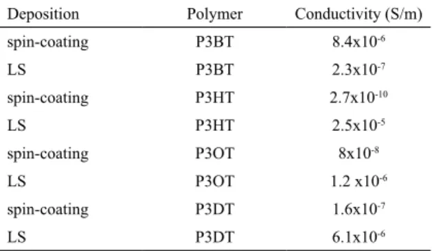
Table 2. Electrical conductivity values for thin ilms of P3AT
derivatives deposited by spin-coating and LS.
Deposition Polymer Conductivity (S/m)
spin-coating P3BT 8.4x10⁻⁶
LS P3BT 2.3x10⁻⁷
spin-coating P3HT 2.7x10⁻¹⁰
LS P3HT 2.5x10⁻⁵
spin-coating P3OT 8x10⁻⁸
LS P3OT 1.2 x10⁻⁶
spin-coating P3DT 1.6x10⁻⁷
LS P3DT 6.1x10⁻⁶
ordered structures, thus hampering the transport of charge carriers in the semiconductor and at the interface between the semiconductor and electrodes23.
Unlike other P3AT derivatives, the P3BT thin ilm deposited by spin-coating showed a higher electrical conductivity compared to that deposited by LS. The ilms deposited by the LS technique generally showed a higher electrical conductivity, probably due to the organization at the molecular level that can be provided by Langmuir techniques24,25. However, the P3BT presented a less eicient adhesion onto the ITO substrate when compared with the other P3AT derivatives. Thus, it is possible that the deposition issues inluenced the layer packaging, thus hampering the mobility of charge carriers and decreasing the electrical conductivity of the LS ilm for P3BT.
4. Conclusions
In summary, the theoretical modeling of the equivalent electrical circuit has been shown to be an important tool for analysis of impedance spectroscopy measurements. The theoretical model used satisfactorily simulates the data obtained for the ITO/P3AT/Al devices. With the analysis of the experimental/theoretical spectra and the values of the parameters used in the equivalent electric circuit, information was obtained and related to electronic transport properties and interfacial efects.
For the polymers P3BT, P3HT and P3OT in the ITO/ P3AT/Al structure, the theoretical it shows that the ilms deposited by spin-coating could be itted by two parallel RC, and those deposited by LS should be itted by three parallel RC. The only exception is P3DT, which was itted by three parallel RC regardless of the deposition technique used to build the thin ilm. Among the P3AT ilms, those grown by the LS technique showed a higher electrical conductivity than those deposited by spin-coating probably related to the distinct molecular arrangement provided by the deposition technique, with the only exception being P3BT. For LS ilms, the conductivity was found to decrease with increasing of alkyl chain length.
5. Acknowledgments
The authors are grateful for the inancial support of the Brazilian agencies FAPESP, INEO/CNPq and CAPES.
6. References
1. Bao Z, Dodabalapur A, Lovinger AJ. Soluble and processable
regioregular poly(3-hexylthiophene) for thin ilm ield-efect
transistor applications with high mobility. Applied Physics Letters. 1996;69(26):4108-4110. DOI: 10.1063/1.117834.
2. Boman M, Stafstr̈m S, Bŕdas JL. Theoretical investigations of the aluminum/polythiophene interface. Journal of Chemical
Physics. 1992;97(12):9144-9153. DOI: 10.1063/1.463340.
3. Babel A, Jenekhe SA. Alkyl chain length dependence of the
ield-efect carrier mobility in regioregular poly(3-alkylthiophene)
s. Synthetic Metals. 2005;148(2):169-173. DOI: 10.1016/j. synthmet.2004.09.033.
4. Bai H, Shi G. Gas sensors based on conducting polymers.
Sensors (Basel). 2007;7(3):267-307.
5. Yu G, Gao J, Hummelen JC, Wudl F, Heeger AJ. Polymer
Photovoltaic Cells: Enhanced Eiciencies Via a Network of Internal
Donor-Acceptor Heterojunctions. Science. 1995;270(5243):1789-1791. DOI: 10.1126/science.270.5243.1789.
6. Ohshita J, Tada Y, Kunai A, Harima Y, Kunugi Y. Hole-injection
properties of annealed polythiophene ilms to replace PEDOT-PSS
in multilayered OLED systems. Synthetic Metals. 2009;159(3-4):214-217. DOI: 10.1016/j.synthmet.2008.09.002.
7. Chang JB, Liu V, Subramanian V, Sivula K, Luscombe C, Murphy A, et al. Printable polythiophene gas sensor array for low-cost electronic noses. Journal of Applied Physics. 2006;100(1):014506. DOI: 10.1063/1.2208743.
8. McNeill CR, Halls JJM, Wilson R, Whiting GL, Berkebile
S, Ramsey MG, et al. Eicient Polythiophene/Polyluorene
Copolymer Bulk Heterojunction Photovoltaic Devices: Device
Physics and Annealing Efects. Advanced Functional Materials. 2008;18(16):2309-2321. DOI: 10.1002/adfm.200800182.
9. Clarke TM, Ballantyne AM, Nelson J, Bradley DDC, Durrant JR. Free Energy Control Of Charge Photogeneration in Polythiophene/
Fullerene Solar Cells: The inluence of Thermal Annealing
on P3HT/PCBM Blends. Advanced Functional Materials. 2008;18(24):4029-4035. DOI: 10.1002/adfm.200800727.
10. Zribi A, Fortin J, eds. Functional Thin Films and Nanostructures
for Sensors: Synthesis, Physics, and Application. New York: Springer; 2009. DOI: 10.1007/b138612.
11. Sanfelice RC, Gonçalves VC, Balogh DT. Langmuir and Langmuir-Schaefer Films of Poly(3-hexylthiophene) with Gold Nanoparticles and Gold Nanoparticles Capped with 1-Octadecanethiol. TheJournal of Physical Chemistry C. 2014;118(24):12944-12951. DOI: 10.1021/jp503083k.
12. Jayaraman S, Yu LT, Srinivasan MP. Polythiophene-gold nanoparticle hybrid systems: Langmuir-Blodgett assembly of
881
Study of the Nanostructure Efect on Polyalkylthiophene Derivatives Films Using Impedance Spectroscopy
13. Johnson BW, Read DC, Christensen P, Hamnett A, Armstrong RD. Impedance characteristics of conducting polythiophene
ilms. Journal of Electroanalytical Chemistry. 1994;364(1-2):103-109. DOI: 10.1016/0022-0728(93)02923-6.
14. Barsoukov E, Macdonald JR, eds. Impedance Spectroscopy:
Theory, Experiment, and Appplications. Hoboken: John Wiley & Sons; 2005. 616 p.
15. Chinaglia DL, Gozzi G, Alfaro RAM, Hessel R. Espectroscopia de impedância no laboratório de ensino. Revista Brasileira de Ensino de Física. 2008;30(4):4504.
16. Chen CC, Huang BC, Lin MS, Lu YJ, Cho TY, Chang CH, et al.
Impedance spectroscopy and equivalent circuits of conductively
doped organic hole-transport materials. Organic Electronics. 2010;11(12):1901-1908. DOI: 10.1016/j.orgel.2010.09.005.
17. Olivati CA, Ferreira M, Carvalho AJF, Balogh DT, Oliveira Jr ON, von Seggern H, et al. Polymer light emitting devices with
Langmuir-Blodgett (LB) ilms: Enhanced performance due to an
electron-injecting layer of ionomers. Chemichal Physics Letters. 2005;408(1-3):31-36. DOI: 10.1016/j.cplett.2005.03.144.
18. Braunger ML, Barros A, Ferreira M, Olivati CA. Electrical
and electrochemical measurements in nanostructured ilms of
polythiophene derivatives. Electrochimica Acta. 2015;165:1-6. DOI: 10.1016/j.electacta.2015.02.232.
19. Nalwa HS, ed. Handbook of Surfaces and Interfaces of Materials. San Diego: Academic Press; 2001.
20. Lange U, Mirsky VM. Separated analysis of bulk and contact resistance of conducting polymers: Comparison of simultaneous two- and four-point measurements with impedance measurements.
Journal of Electroanalytical Chemistry. 2008;622(2):246-251. DOI: 10.1016/j.jelechem.2008.06.013.
21. Salleo A. Charge transport in polymeric transistors. Materials Today. 2007;10(3):38-45. DOI: 10.1016/S1369-7021(07)70018-4.
22. Kline RJ, McGehee MD, Kadnikova EN, Liu J, Fŕchet JMJ.
Controlling the Field-Efect Mobility of Regioregular Polythiophene
by Changing the Molecular Weight. Advanced Materials. 2003;15(18):1519-1522. DOI: 10.1002/adma.200305275.
23. Park YD, Kim DH, Jang Y, Cho JH, Hwang M, Lee HS, et
al. Efect of side chain length on molecular ordering and ield-efect mobility in poly(3-alkylthiophene) transistors. Organic Electronics. 2006;7(6):514-520. DOI: 10.1016/j. orgel.2006.07.007.
24. Li G, Shrotriya V, Huang J, Yao Y, Moriarty T, Emery K, et
al. High-eiciency solution processable polymer photovoltaic
cells by self-organization of polymer blends. Nature Materials. 2005;4:864-868. DOI: 10.1038/nmat1500.