Three cell flying capacitor inverter for dielectric barrier discharge plasma applications
A. Flores-Fuentesa, R. Pe˜na-Eguiluzb,∗ L´opez-Callejasa,b, A. Mercado-Cabrerab, R. Valencia-Alvaradob, S. R. Barociob, and A. de la Piedad-Beneiteza
aInstituto Tecnol´ogico de Toluca, Av. Tecnol´ogico S/N,
A.P. 890, Toluca, M´exico and
bInstituto Nacional de Investigaciones Nucleares, Plasma Physics Laboratory, A.P. 18-1027, C.P. 11801, M´exico D.F., M´exico (Received on 25 November, 2008)
It is reported the design, construction and initial tests of a three cell flying capacitor inverter (TCFCI) in a half-bridge configuration. The device operates at a 200 kHz frequency which leads to a voltage output at 12.5 kHz presenting an acceptable response in an open-loop configuration. These features outdo those reported in the current multilevel converter literature. The TCFCI is driven by pulse width modulation, following a phase shift (PS-PWM) control strategy, in order to generate a steady AC voltage signal. This inverter is used to excite a dielectric barrier discharge cell (DBDC) intended for cold plasma generation at room pressure. Some results obtained for two different kinds of atmosphere, helium and argon, are presented. All the system having been tested, early recorded voltage and current waveforms, are included. Finally, three methods for calculating the related electric efficiency of the discharge cell are discussed.
Keywords: DC-AC power converters, multilevel inverters, electric discharges, plasma
I. INTRODUCTION
Dielectric barrier discharges (DBD) also known as silent discharges, are commonly produced in parallel plates or coax-ial cells at near atmospheric pressure (1-3 atm). Plasmas in a dielectric barrier discharge cell (DBDC) are generated by applying high voltage (HV) to a pair of electrodes, separated by a gap, where at least one of these is covered by a dielectric sheet, usually made of quartz, glass or ceramic. These dis-charges are frequently used in industrial ozone generation [1] or in the treatment of air pollutants [2], in particular, solvents or volatile organic compounds (VOC) which are mainly pro-duced around chemical plants [3]. The conditions required to produce non-equilibrium plasmas are easier to attain with DBDC than by alternative methods such as low pressure dis-charges, high pressure discharges with fast pulses, or elec-tron beam injection. DBD are generated in a high pressure gas and consist of a multitude of short lived current filaments [4]. Due to the short duration of these micro discharge chan-nels and the prevailing low ion mobility, the kinetic energy in silent discharges is principally transferred to electrons, which become hot, unlike the other species. This behavior provides a significant electronic excitation of molecules. As a conse-quence, the plasma promotes efficient thermo chemical reac-tion processes, which are desirable in the destrucreac-tion of haz-ardous organic compounds [5]. In order to achieve a stable DBD performance, the incumbent power sources usually pro-vide HV AC, from some tens of Hz [6] up to the order of sev-eral kHz [7] with amplitudes from 1 to 100 kV. Thus, sevsev-eral authors have resorted to resonant inverters either in a half-bridge configuration [8] or in a full-half-bridge one, operating at tens of kHz [9]. Nevertheless, these converters, however effi-cient, are constrained to operate in a narrow frequency range. The present report presents some early results of a complex system which is mainly constituted by a DBDC made of par-allel plates biased by a coupled transformer whose primary is driven by a voltage source inverter (VSI) configured on
∗Electronic address:[email protected]
the basis of a half-bridge three cell flying capacitor inverter (TCFCI). Pulse width modulation by means of phase shift-ing (PS-PWM) has been applied in order to drive the TCFCI. The latter has been implemented through a hybrid electronic circuit, which generates six commutation pulses for the high power switches that constitute the TCFCI. An appropriate op-erating system provides a four-level chopped voltage at the output inverter. The correct performance of the control strat-egy enables a good open-loop inverter behavior due to a nat-ural balance originated in the inherent current harmonics. An electrical characterization of the system, including efficiency calculations, has been included.
II. SYSTEM DESCRIPTION
The electric circuit representation of the proposed DBD system is shown in Fig. 1. It is mainly composed by a variable autotransformer supplying an adjustable AC voltage level within 0-220 V to a non controlled full wave rectifying bridge. It delivers in turn a DC voltage to a voltage divider constituted by two capacitors,CS1andCS2, along with aCS f one, functioning like input filter. Thus, a bipolar DC volt-age is applied to the input of a TCFCI which is assembled by means of three commutation cells. Each one of the last is im-plemented with a couple of complementary switches, namely: (T1,T1’), (T2,T2’) and (T3,T3’) respectively. These are high-frequency high-voltage MOSFET’s associated to free wheel-ing diodes and separated by a floatwheel-ing voltage source. Each one of the flying capacitorsC1andC2are connected between two different commutation cells. The capacitors operate as an ideal voltage supply whereby the averaged current must vanish. It is accomplished when the inverter maintains a bal-anced voltage distribution between these capacitors by apply-ing identical work cycles to the switches. The number of ca-pacitors determines directly the amount of voltage levels that the converter is able to handle. Assuming an identical capac-itance: C=C1=C2, then the voltage across each capacitor VCkis given byVCk=
k
defined byVC1 =
1
3V andVC2 =
2
3V respectively. Meanwhile, the capacitance value can be determined as:
Ck= ISmax p fSW∆VCk
(1) where:∆VC
k is the maximum permissible ripple voltage pro-vided by the floating capacitor,ISmaxis the maximum DC cur-rent inverter and, fSWis the switching frequency. A converter operation guaranteeing open loop stability is determined by two main factors: (i) an adequate sequence of the commuta-tion pulses imposed to the power switches and (ii) the correct effective voltage levelsVCkamong flying capacitors.
FIG. 1: Diagramme of the implemented DBD system
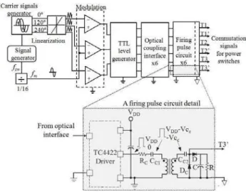
FIG. 2: Block diagram of the implemented PS-PWM technique and a detailed conditioning switch gate pulse circuit
The TCFCI output voltage is applied to the DBDC, herein modeled by a parallel circuit composed by a capacitorCfand the primary winding of an isolation step-up (1:30) HV trans-former. The proposed electric model of the DBDC is char-acterized by:Cdwhich represents the equivalent capacitance
of the dielectric sheets placed in both electrodes. Cgis the gas capacitance,Rgis the plasma sheet resistance, andGpis a voltage-controlled current source reproducing the exponen-tial growth of the discharge currentidis(t)when the voltage across the cell,vs(t), surpasses the breakdown threshold volt-ageVb. Csis the stray capacitance present in the real equip-ment.
A PS-PWM strategy was chosen in order to modulate the pulses width applied to VSI power switches as seen in Fig. 2. The system is supported by a sinusoidal waveform generator which provides a referencefSW = 200 kHz signal to an opera-tional amplifiers stage, where three23πout of phase sinusoidal
signals are generated. The latter are applied to a logarithmic amplifier stage, which in turn produces triangular waveforms meant to act as carrier signals to be compared to the modulat-ing one (produced by a digital frequency divider, and later on integrated, so to obtain a sinusoidal waveform with frequency fm= 161 fSW = 12.5 kHz). The modulation process is devel-oped by comparing the modulating sinusoidal signal and the triangular waveforms, resulting in three different sequences of pulses which are conditioned in order to meet TTL lev-els. After that, the resulting pulses are optically isolated be-tween the command circuit and the power switches by means of optic fiber link connections reducing the electromagnetic interference (EMI). Likewise, another circuit has been imple-mented with a magnetic coupling provided that the firing sig-nal of each power switch should be applied with respect to a floating voltage. Thus, driver outputs are coupled by means of pulse transformers and commutation signals, given that the switches need additional components, as it is shown in the fir-ing circuit detail of Fig. 2. There, capacitorCC1provides the restoration voltage for the inductance of the primary wind-ing transformer; both of these components integratwind-ing anLC circuit. Thus a resistorRC is added with the purpose of pre-venting any resonant effect. Additionally, capacitorCC2along with diode DC are used to re-establish the driver’s original amplitude. Finally, the circuit containing capacitorC, resis-torR and diode D modifies the dynamical behavior of the pulse signal provided from the secondary winding of the pulse transformer.
An implemented Simulink/MatlabR model of the pro-posed system makes possible to obtain a valuable approach-ing of its dynamic performance. As the simulation outcome in Fig. 3.a depicts, three triangular mutually 23πout of phase
FIG. 3: Simulation outcome from the implemented modulation strat-egy circuit: (a) the three carrier signals are compared with respect to the modulating signal; (b) resulting sequences to be applied as control signals to the power switches
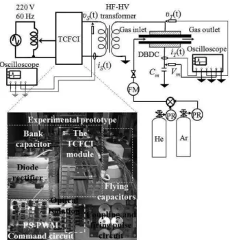
III. EXPERIMENTAL SET-UP
The instrumental arrangement used in this study is repre-sented in Fig. 5, where several photos of previously described TCFCI circuits can be identified. A top down view of the im-plemented DBDC is depicted in Fig. 6.a; meanwhile, Fig. 6.b illustrates the inner cell structure. The DBDC is constituted by two electrodes of 0.12 m diameter made of aluminum sep-arated by two glass dielectric sheets, 0.002 m thick, and a gapl = 0.002 m between them. Thus, the total cell capac-itance of the DBDC is given by an equivalent capaccapac-itance Cd=ε0εrS/2l, where the industrial glass dielectric relative permittivity isεr = 4.9, ε0 = 8.8541×10⁻¹² F/m is the per-mittivity in vacuum, andS= 0.0113 m2is the total calculated electrode surface. Hence, the DBDC calculated capacitance turns out to beCd= 122 pF. The gas capacitanceCgwas cal-culated for argon and helium, in both cases its magnitude be-ing near 50 pF. The DBDC gas supply was endowed with a pipeline connected from two gas containers through a gas mixer and mass flow meters. In all cases, electric discharges were generated at atmospheric pressure with gas mass flow of 2.0 LPM.
FIG. 4: Simulation outcome of the primary winding voltage sup-ply and resulting current intensity. (b) Applied cell voltage and its resulting current in the case of an argon discharge
FIG. 6: (a) Top down view of the operational DBDC, and (b) schematic representation of the DBDC cross section
The TCFCI output voltage and current (vp(t),ip(t)) and DBDC applied voltage and discharge current (vs(t),is(t)) are monitored by means of a (Tektronix TDS2014) oscilloscope equipped with a HV probe (Tektronix P6015) and a current sensor (Stangenes model 0.5-1.0 W). We consider as an il-lustration the DBDC applied voltage and its resulting current waveform (vp(t),ip(t)) captured during the stable phase of the discharge, shown in Fig. 7. From these waveforms, the peak values ofvpabout 28 V and ofipabout 5.8 A have been determined. Thus, real power applied to the primary winding of the transformer is given by:
Pp(t) =vp rms(t)·ip rms(t)·cos(θ) (2)
which, considering that measured value ofθ= 850, amounts
toPp(t)≈7.1 W: an expected result as the DBDC exhibits a predominantly capacitive conduct.
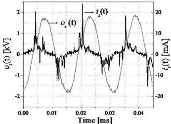
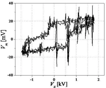
Fig. 8 portrays the voltage and current wave forms mea-sured at the DBDC plugs. Thevs(t)peak value reaches about 1.75 kV while that ofis(t)is 5 mA, estimated from its first harmonic. Although the instantaneous power absorbed by the DBDC can be directly assessed from the product ofvs(t) andis(t), it can also be assessed from the charge stored in the cell, Qs(t) (here represented by the measured voltage vm(t) of a reference capacitanceCm, keeping in mind that Qs(t) =Cmvm(t)) versus the applied voltage,vs(t) (Fig. 9) [12],[13]. In this work we considered thatCm∼2µF is the reference capacitance shown in Fig. 5,Vmis the voltage
am-FIG. 7: Experimental waveforms of the applied voltagevp(t)and of the resulting current intensityip(t), in the case of a 2 LPM argon flow at room pressure.
FIG. 8: Waveforms ofvs(t)andis(t)at the DBDC operating with a 2 LPM argon flow at room pressure.
plitude per division on the vertical axis of Fig. 9, namely 20 mV/div, andVs1 kV/div is the magnitude of a division on the horizontal axis. Thus, the computed energy stored by the cell E= 0.196 mJ while the power supplied to the cellPC= f E, where f is the frequency of the excitation signal applied to the DBDC, namely,PC = 2.45 W. In other words, the power transferred from the transformer secondary to the cell attains an electric efficiency of 34.5% in the case of argon discharges. Thevp(t)peak level, which is about 12.5 V, and the cor-respondingip(t)peak, around 3 A, have been obtained from the characteristic signals applied to the transformer primary as seen in Fig. 10 in the case of a helium discharge. Thus, the real power applied to the primary winding, considering thatθ= 850 leads to a valuePp(t)≈2.61 W. The signal in
the DBDC is depicted in Fig. 11. The peak value ofvs(t)is around 1 kV, and, approachingis(t)by its first harmonic, its maximal value reaches 2 mA.
FIG. 9:vm(t)versusvs(t)Lissajous wave form in the DBDC with a 12.5 kHz excitation frequency when fed with argon.
FIG. 10: Experimental time patterns of the applied voltage vp(t) and its associated currentip(t), in a 2 LPM flow of helium at room pressure
FIG. 11:vs(t)andis(t)time patterns measured in the DBDC, work-ing on a 2 LPM helium flow at room pressure
the one shown in Fig. 12, thenVm=10 MV/div,Vs=1 kV/div, wherebyEC=20µJ/div2and, consequentially,E = 0.045 mJ. Finally,PC=0.562 W so that the power transferred from the primary to the cell can be estimated as 21.53%.
FIG. 12:vm(t)versusvs(t)waveform of a DBDC with helium and a 12.5 kHz excitation frequency
A second method for calculating the power consumed by the DBDC yields the following Manley expression [13]:
Pc=4VbCdf
VM−Vb
C
d+Cg Cd
(3) where:VM is the maximal amount of voltage supplied to the cell. Consequentially, operating it on argon requires 2.64 W which implies an 34.6% efficiency while, in helium, the re-quired power, 0.564 W, improves the efficiency up to 21.6%.
FIG. 13: Waveforms of the instantaneous powervs(t)·is(t)applied to the DBDC with a 2 l/min argon flow at room pressure
FIG. 14: Waveforms of the instantaneous powervs(t)·is(t)applied to the DBDC with a 2 l/min helium flow at room pressure.
suggested by Fig. 13 (argon) and Fig. 14 (helium). In a simi-lar fashion, Table I gathers the results of the power estimation by all three methods including the respective efficiency values with both gases.
It is obvious that the first and third methods seem to agree better, which could be expected from their being obtained from experimental values. In contrast, the second one de-pends on the breakdown voltage, rather roughly estimated from the experimental conditions.
IV. CONCLUSIONS
The design TCFCI built out of high power high frequency semiconductors intended to generate room pressure dielec-tric barrier discharges has been described. Its hybrid system of command consists of a relatively simple and stable cycle which simplifies the handling of reference signals in order to accomplish the required power switch commutation through
intermediate circuits able to isolate the low power stage from the high one. Thus, the use of an insulation stage reduces electromagnetic interference significantly along with the tran-sients typical of the high power systems.
The open loop operation of the proposed system maintains a stable behaviour conducive to a well ordered voltage distri-bution in the floated capacitors given the selected modulation technique. Although the proposed design allows one to adjust the frequency of the reference sinusoidal signal so to mod-ify the DBDC excitation frequency, the 12.5 kHz frequency was maintained throughout the study provided that this is the maximal possible value for the whole system. Thus, when a different modulation system is in place, e.g., a square pulse one, it is possible to raise the frequency even further with the consequent improvement in the general efficiency, albeit with some change of components.
The static converter developed for the DBDC discharge generation has been satisfactorily tested by establishing room pressure discharges in a parallel plate cell containing helium and argon, achieving efficiencies above 20 and 30 respec-tively. An innovative conversion characteristic of the pro-posed TCFCI is its high 12.5 kHz operation frequency, far beyond the 3 kHz one reported in similar inverters.
TABLE I: Comparison of power values applied to the DBDC and their resulting efficiency according to three distinct calculation
procedures
Acknowledgements
This work received partial financial support from CONA-CYT and DGEST, Mexico. The authors are very grateful for the technical collaboration received from M. T. Torres M., I. Contreras V. and P. Angeles E.
[1] C. Gottschalk, J. A. Libra and A. Saupe, Ozonation of Water and Waste Water: A Practical Guide to Understanding Ozone and its Applications, Wiley-VCH; Weinheim (2000).
[2] C. H. Wang, G. F. Li, Y. Wu, Y. Wang, J. Li, D. Li and N. H. Wang, Plasma Chem. Plasma P.27, 1, 65 (2007).
[3] O. Godoy-Cabrera, R. L´opez-Callejas, R. Valencia, A. Mu˜noz-Castro, S. R. Barocio, E. Ch´avez A., A. Mercado-Cabrera, A. de la Piedad-Beneitez, B. Rodr´ıguez-M´endez and J. Rodr´ıguez-Arce, Braz. J. Phys.34, 4B, 1766 (2004).
[4] U. Kogelschatz, B. Eliasson and W. Egli, J. Phys. IV France,1997,7, C4, 47 (1997).
[5] L. A. Rosocha, Processing of Hazardous Chemical Using Silent-Discharge Plasmas, in Environmental Aspects in Plasma Science, Ed. W. Manheimer,American Institute of Physics Press, New York, (1997).
[6] J. Velikonja, J. A. Robinson, M. A. Bergougnou, J. S. Peter-Castle, W. L. Cairns and I. I. Inculet, Proc. IEEE International Symposium on Electrical Insulation, Anaheim CA, USA, 2-5
April,1, 25 (2000).
[7] D. Evans, L. A. Rosocha, G. K. Anderson, J. J. Coogan and M. J. Kushner, J. Appl. Phys.74, 9, 5378 (1993).
[8] O. Godoy-Cabrera, J. S. Ben´ıtez-Read, R. L´opez-Callejas and J. O. Pacheco-Sotelo, Int. J. Electron.87, 3, 361 (2000). [9] O. Godoy-Cabrera, J. S. Ben´ıtez-Read, R. L´opez-Callejas, J. O.
Pacheco-Sotelo and A. de la Piedad-Beneitez, Int. J. Electron.
92, 6, 327 (2005).
[10] F. Hamma, T. A. Meynard , F. Tourkhani and P. Viarouge, Proc. IEEE Power Electronics Specialists Conf. (PESC ’95), Atlanta, USA, 18-22 June,2, 1208 (1995)
[11] N. Naude, J. P. Cambronne, N. Gherardi and F. Massines, J. Phys. D: Appl. Phys.38, 530 (2005).
[12] Z. Falkenstein and J. J. Coogan, J. Phys. D: Appl. Phys.30, 817 (1997).