COMPACT YET EFFICIENT HARDWARE ARCHITECTURE FOR
MULTILAYER-PERCEPTRON NEURAL NETWORKS
Rodrigo Martins da Silva
∗ [email protected]Nadia Nedjah
∗ [email protected]Luiza de Macedo Mourelle
† [email protected]∗Department of Electronics Engineering and Telecommunications
State University of Rio de Janeiro Rio de Janeiro, Brazil
†Department of Systems Engineering and Computation
State University of Rio de Janeiro Rio de Janeiro, Brazil
RESUMO
Arquitetura de hardware compacta e eficiente para redes neurais artificiais do tipo múltiplas camadas
Em termos computacionais, uma rede neural artificial (RNA) pode ser implementada em software ou em hardware, ou ainda de maneira híbrida, combinando ambos os recursos. O presente trabalho propõe uma arquitetura dehardwarepara a computação de uma rede neural do tipo perceptron com múl-tiplas camadas (MLP). Soluções emhardwaretendem a ser mais eficientes do que soluções emsoftware. O projeto em questão, além de explorar fortemente o paralelismo das redes neurais, permite alterações do número de entradas, número de camadas e de neurônios por camada, de modo que diversas aplicações de RNAs possam ser executadas nohardware pro-posto. Visando a uma redução de tempo do processamento aritmético, um número real é aproximado por uma fração de inteiros. Dessa forma, as operações aritméticas limitam-se a operações inteiras, executadas por circuitos combinacionais. Uma simples máquina de estados é demandada para contro-lar somas e produtos de frações. A função de ativação usada neste projeto é a sigmóide. Essa função é aproximada me-diante o uso de polinômios, cujas operações são regidas por
Artigo submetido em 10/03/2011 (Id.: 01299) Revisado em 06/05/2011, 19/07/2011
Aceito sob recomendação do Editor Associado Prof. Carlos Roberto Minussi
somas e produtos. Um teorema é introduzido e provado, per-mitindo a fundamentação da estratégia de cálculo da função de ativação. Dessa forma, reaproveita-se o circuito aritmé-tico da soma ponderada para também computar a sigmóide. Essa re-utilização dos recursos levou a uma redução drás-tica de área total de circuito. Após modelagem e simula-ção para validasimula-ção do bom funcionamento, a arquitetura pro-posta foi sintetizada utilizando recursos reconfiguráveis, do tipo FPGA. Os resultados são promissores.
PALAVRAS-CHAVE: Redes neurais artificiais, hardware para redes neurais, sigmóide, paralelismo, FPGA.
ABSTRACT
computa-tion, a real number is represented using a fraction of integers. In this way, the arithmetics is limited to integer operations, performed by fast combinational circuits. A simple state ma-chine is required to control sums and products of fractions. Sigmoid is used as the activation function in the proposed implementation. It is approximated by polynomials, whose underlying computation requires only sums and products. A theorem is introduced and proven so as to cover the arith-metic strategy of the computation of the activation function. Thus, the arithmetic circuitry used to implement the neuron weighted sum is reused for computing the sigmoid. this re-source sharing decreased drastically the total area of the sys-tem. After modeling and simulation for functionality vali-dation, the proposed architecture synthesized using reconfig-urable hardware. The results are promising.
KEYWORDS: Artificial neural networks, hardware for neural networks, sigmoid, parallelism, FPGA.
1
INTRODUCTION
An artificial neural network (ANN) is an attractive tool for solving problems such as pattern recognition, generaliza-tion, predicgeneraliza-tion, function approximageneraliza-tion, optimization and non–linear system behavior mapping. When dealing with an ANN implementation, systems based on hardware are usually faster than software alternatives (Zurada, 1992; Ro-jas, 2010; Zhu and Sutton, 2003; Dias et.al, 2004; Omondi and Rajapakse, 2008).
When a particular task does not require so much speed, a software-based neural network system can be sufficient and satisfactory in running the task, through a PC or a general-purpose processor. ANN systems based on software do not demand much design effort. On the other hand, ANNs pro-vide an adequate research field for applying the parallel com-putation and, of course, this parallelism can be best explored in a hardware-based implementation (Chen, 2003; Omondi and Rajapakse, 2008). So, a hardware architecture can be devised in order to use the massive parallelism provided in the neuron–layer computation. Circuit components can be designed and adequately mapped to exploit details from both the arithmetic computation and control process.
The Hardware designed, in this work, can be used by any neural network applications. It supports ANNs with different number of layers, neurons per layer and inputs. This is one of the proposed hardware main features: flexibility through andon-the-flyreconfigurability. To perform a multilayer per-ceptron neural network (MLP), the hardware requires the fol-lowing parameters:
1. The number of inputs of the network. Letimaxbe this number;
2. The number of layers of the network. Letlmaxbe this number;
3. The number of neurons per layer. Letnibe this number, whereirepresents theithlayer:i= 1,2, . . . , l
max;
4. If at least one neuron of a certain layer is going to op-erate with a bias, parameterbiasof such layer must be on.
A neural network usually has more than one layer. Nev-ertheless, the proposed hardware provides only one single physical layer, ahardware layer, which performs the entire computation due to all the layers of the ANN by reusing the neurons of this unique physical layer. In this context, the neural network layers are named virtual layers. Note that this is done without loss of performance as the computation due to the ANN layers are data-dependent, and thus need to be executed sequentially. This strategy reduces the designed circuit area. Note that there exists an overhead due to the re-quired control to use a single physical layer. However, the time spent is minimal and so has a very little impact on the overall performance of ANN hardware. The time spent com-puting the weighted sum and activation function is far longer than that spent controlling the layers computation. Moreover, the neurons of the physical layer operate in parallel to per-form the required computation. For instance, weighted sums are computed by all hardware neurons at the same time, and so is the case of the computation of the activation function. Hence, the overall processing time of the ANN is also re-duced.
Whenever a digital hardware is designed with some simi-lar circuit blocks, it reveals a feature which is very attrac-tive to an implementation inField Programmable Gate Array (Wolf, 2004). Since all hardware neurons are digital circuits that are literally equal, the synthesis of the hardware layer in a FPGA is easily and best achieved.
In this work, a real number is represented as a fraction of in-tegers (Santi-Jones and Gu, 2008). Floating-point represen-tation based on the IEEE-754 standard (Tanenbaum, 2007) is not used here. Mathematic operations, such as sums and multiplications, using floating-point numbers require specific routines and, in terms of hardware design, a circuit that needs very large silicon area to be implemented. Also, long com-puting time is also demanded (Nedjah et al., 2008).
hardware is used and a simple finite state machine would rule those integer operations.
A neuron weighted sum is a set of sums and multiplications of fractions. The activation function used in this work is the logistic sigmoid, which is approximated by quadratic poly-nomials. These are derived from a curve-fitting method:least mean squares. This is done, in contrast with using alookup table, which is known to compromise the neuron rendered re-sult. The quadratic polynomial-based approximation yields a far more precise result.
Provided that the sigmoid is approximated by second-degree polynomials, only sums and multiplications are needed to get the final result. Thereby, the circuit, once designed to compute weighted sums, can be reused for computing the sigmoid function, without extra effort or cost. This strategy spared unnecessary circuit, which lead to area extension and motivated by increasing the precision of the neuron rendered results (Martins et al., 2009).
This paper is organized as follows: First, in Section 3, we describe the data representation used in this design as well most arithmetic operations. Then, in Section 4, we describe the sigmoid computation. Subsequently, in Section 5, the overall hardware architecture and controllers are presented. Thereafter, in Section 5.1, The hardware neuron layer is de-picted and discussed. Next, in Section 5.1.1, we show and comment on the neuron circuit design. After that, in Section 6, we report some simulation and synthesis result and discuss them. Finally, in Section 7, we draw some conclusion about the reported work and point out some future directions and improvements.
2
RELATED WORK
Research in the area of neural networks have been ongo-ing for over two decades now and hence the are many related work published. There are many work surveys published (Moerland and Fiesler, 1997; Lindsey and Lind-blad, 1994; Rojas, 2010). In (Zhang and Pal, 2002.), the au-thors report on an efficient systolic implementation of ANNs. In (Kung, 1988; Kung and Hwang, 1989), the authors de-scribe a novel scheme for designing special purpose systolic ring architectures to simulate feed forward stage is artificial neural networks. In (Kung, 1988), the authors present in-teresting results on implementing the back propagation al-gorithm on CMU Warp. In (Ferrucci, 1994), the author de-scribes a multiple chip implementation of ANNs, using basic building blocs, such as multipliers and adders. In (Nedjah et al., 2009), the authors also take advantages of MAC (mul-tiply and Accumulate) hard cores implemented into the fab-rics of the FPGA to implement efficiently sums and prod-ucts that are necessary in the ANN underlying
computa-tions. In (Beuchat et. al., 1998), the authors developed an FPGA platform, called RENCO - a REconfigurable Net-work COmputer. In (Bade and Hutchings, 1994; Nedjah and Mourelle, 2007), the authors report an implementation of stochastic neural networks based on FPGAs. Both imple-mentations result in a very compact circuit. In (Zhang et. al., 1990), the author presents an efficient implementation of the back propagation algorithm on the connection machine CM-2. In (Botros and Abdul-Aziz, 1994), the author intro-duce a system for feed forward recall phase and implement it on an FPGA. In (Linde et. al., 1992), the authors describe REMAP which is an implementation of whole neural com-puter using only FPGAs. In (Gadea et. al., 2000), the au-thors report on a pipelined implementation of an on-line back propagation network using FPGA. In (Canas, et al., 2008), the authors propose a hardware implementation of ANNs, where the activation function is discretized and stored in a lookup table.
Many analog hardware implementations of ANNs have also been reported in the literature. In general, the implementa-tion are very fast, dense and low-power when compared to digital ones, but they come along with precision, data stor-age, robustness and learning problems, as shown in (Holt and Baker, 1991; Nedjah et al., 2011; Choi et. al., 1996). It is an expensive and not flexible solution, as any ASIC (Montalvo et. al., 1997).
3
NUMERIC REPRESENTATION
A neural network operates with real numbers. Fixed–point representation implies a great accuracy loss. Floating–point notation (IEEE-745) offers good precision, but requires a considerable silicon area and a considerable time for arith-metic computing.
Searching for speed and circuit area trade-off, the alternative chosen to represent a real number was theFractional Fixed Point, where a Fraction of integers is used to represent a real number (Santi-Jones and Gu, 2008). This model is depicted in Figure 1, showing the binary structure of a general frac-tion. This piece of data has 33 bits. 17th bit of the least significant bits is for the algebraic sign of the fraction.
Numerator (N) Denominator (D)
15..0 16
32..17
17 bits 16 bits
Sign Bit
N
D
A real float number converted to a fraction is shown in Eq. 1. Such fraction in its binary structure is also shown in Figure 2.
−0,0031771247021445607→ 12
−3777 (1)
N
a= 12
D
a=
−
3777
17 bits 16 bits
Sign Bit
0000000000001100 1 0000111011000001
Figure 2: Example of number represented using a fraction
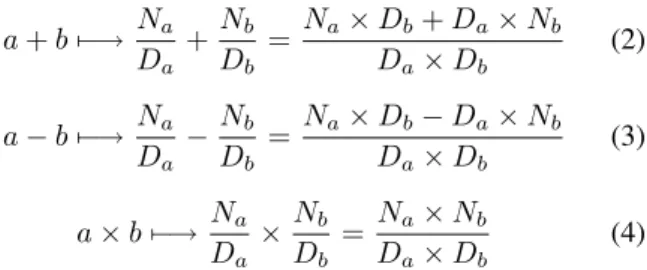
Regardingaandbreal numbers, Equations 2, 3 and 4 display most of the arithmetic operations performed by the hardware. Neuron weighted sum and sigmoid computing are based on sums or subtractions and multiplications of fractions.
a+b7−→ Na Da
+Nb
Db
= Na×Db+Da×Nb
Da×Db
(2)
a−b7−→ Na Da
−Nb Db
= Na×Db−Da×Nb
Da×Db
(3)
a×b7−→ Na Da
×Nb Db
= Na×Nb
Da×Db
(4)
There is an advantage of using fractions: a sum or a mul-tiplication of two fractions is achieved through a mere se-quence of integer operations, which require simple combina-tional circuits (Uyemura, 2002).
A sum of two fractions, for instance, demands 3 multiplica-tions and 1 addition of integers: an unsophisticated finite– state machine is used to command the combinational com-puting sequence. Combinational Adder and multiplier pro-vide attractive response timing and are easily allocated on FPGAs (Wolf, 2004).
3.1
Adaptive number framing technique
A fraction that results from a sum or product of two other fractions might require a bit range that exceeds the width of the binary structure of Figure 1. Repeated fraction operations would demand unlimited number of bits to keep up with the highest result precision. This is certainly impracticable. One possible and common solution is atruncation.
0000000000000110 1101110111100111 = 450023 0000000000000110 = 6 0000000000010011 1000010000110110 = 1279030
0000000000010011 = 19
Figure 3: Direct framing
For instance, consider two fractions which fit into the binary structure of Figure 1, so that their multiplication results into the fraction N umDen = 450023
1279030. Neither the numerator nor the denominator would fit in the Figure 1 notation as450023>
65535and1279030>65535. Therefore, such fraction must be adjusted to fit into the binary limitation imposed in the hardware implementation.
The multiplication of two fractions (each one in the form of Figure 1) generates a fraction of 64 bits, in general, whose numerator and denominator are of 32 bits. The proposed hardware does not support this bit length and a framing tech-nique must be thought of, aiming at minimizing the loss of accuracy.
An easy truncation or framing that could be done on 1279030450023 would be to take only the least–significant sixteen bits from numerator and from denominator – as Figure 3 displays – nameddirect framing(the simplest one).
The framing depicted in Figure 3, performed over fraction 450023
1279030 =0.35184. . . , yields 6
19 =0.31578. . . . This tech-nique implies a high precision loss. In this work, anadaptive framing technique is used, where successive one-bit right-shifts of the binary representations of both the numerator and denominator, until the fraction under consideration is framed into the width of the representation of Figure 1, which is the fraction default binary length.
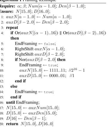
Algorithm 1 describes the steps of the proposed framing technique. It performs the adjustment of N umDen to produce
N
D that fits in the default structure used in this design. Note that N umis a natural ofα > 16bits and Den 6= 0is an integer of β >17bits. Recall that the MSB ofDenis the fraction sign bit. NumeratorN has 16 bits e denominatorD
has 17 bits; The bit MSB ofDis the sign bit of the resulting fraction. Note that the largest number that can be represented is−655351 , . . . ,01,· · ·+655351 . Hence, when the framing operation reaches an all-zero denominator, the largest possi-ble integer is used (see lines 10 and 11 of Algorithm 1.
Algorithm 1Framing technique
Require: α;β;N um[α−1..0];Den[β−1..0]; Ensure: N[15..0];D[16..0];
1: auxN[α−1..0]←N um[α−1..0]; 2: auxD[β−2..0]←Den[β−2..0]; 3: repeat
4: if Or(auxN[(α−1)..16]) || Or(auxD[(β −2)..16])
then
5: EndFraming←false;
6: RightShiftauxN[α−1..0];
7: RightShiftauxD[β−2..0];
8: ifNor(auxD[β−2..0]then
9: EndFraming←true;
10: auxN[15..0]←1111..11; //216−1 11: auxD[15..0]←0000..01; //1
12: end if
13: else
14: EndFraming←true;
15: end if
16: untilEndFraming;
17: N[15..0]←auxN um[15..0]; 18: D[15..0]←auxDen[15..0]; 19: D[16]←Den[β−1];
20: return N[15..0], D[16..0]
bit. This method is worthwhile because it minimize the loss of accuracy. Note that, fraction1279030450023, which evaluates pre-cisely to 0.3518471028, results in 0.3157894736 with a di-rect standard framing while when it yields 1406339969using adap-tive framing, which is equivalent to 0.3518476819. Note that an overall evaluation of precision loss throughout the com-putational process depends on the specific composition of the bits that are being shifted out from the numerator and denominator.
3.2
Precision of the adaptive framing
The loss of precision that is occasioned by a single iteration of the framing procedure described in Algorithm 1 depends on the the bit that is shifted out from the numerator and the corresponding in the denominator. Considering one framing iteration, there 4 possible cases as described below.
1. Both the numerator and denominator are even. i.e.
N um= 2×N+0×20andDen= 2×D+0×20. Thus, we have no loss of precision as explained in Equation 5, whereinE00is the error introduced by right-shifting both the numerator and denominator:
E00= 2N
2D − N
D = 0 (5)
450023
1279030
225011
639515
112505
319757
56252
159878
28126
79939
14063
39969
Figure 4: Adaptive framing
2. Both the numerator and denominator are odd. i.e.
N um= 2×N+1×20andDen= 2×D+1×20. Thus, we have a loss of precision as explained in Equation 6, whereinE11is the error introduced by right-shifting both the numerator and denominator:
E11=
2N+ 1 2D+ 1 −
N D =
D−N
D(2D+ 1) (6)
3. The numerator is even, i.e.N um= 2×N+ 0×20and denominator are odd, i.e.Den= 2×D+ 1×20. Thus, we have a loss of precision as explained in Equation 7, whereinE01is the error introduced by right-shifting both the numerator and denominator:
E01= 2N
2D+ 1 −
N D =
−N
D(2D+ 1) (7)
4. The numerator is odd, i.e.N um= 2×N+ 1×20and denominator are even, i.e.Den= 2×D+0×20. Thus, we have a loss of precision as explained in Equation 8, whereinE10is the error introduced by right-shifting both the numerator and denominator:
E10=
2N+ 1
2D −
N D =
1
2D (8)
Therefore, assuming that it is 0s and 1s are evenly distributed in a binary representation, the average error introduced by a single shift can be evaluated as shown in Equation 9.
Eavg=
4D−4N+ 1
8D(2D+ 1) (9)
The proposed adaptive framing technique provides an ad-equate accuracy for the purpose of this work. The pro-posed hardware has to be equipped with a right-shifter to per-form fraction adjustment. A one-bit right-shift is an integer-divide-by-2 operator. This property is also useful in the moid computation as the strategy used for computing the sig-moid was forged in order to take advantage of the shifter al-ready included in the hardware. This will be explained in the next section.
4
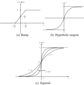
ACTIVATION FUNCTION
f = ϕ(v)
v
1
1 1
2 +2
1 2
+
(a) Ramp
f = ϕ(v)
−1 +1
v
0
(b) Hyperbolic tangent
f = ϕ(v)
+1
v
0 +0,5
a = 0,5
a = 1
a = 2
(c) Sigmoid
Figure 5: Common activation functions
Equation 11 and sigmoid as described in Equation 12. The curves of these three activation functions are shown in Figure 5.
y=ϕ(v) =
1 ifv≥b
1
b−av− a
b−a ifa < v < b
0 ifv≤a
(10)
ϕ(v) =b·e
av−e−av
eav+e−av, (11) whereina6= 0andb6= 0.
ϕ(v) = 1
1 +e−av (12)
The sigmoid is widely used in multilayer-perceptron neural networks (Haykin, 1999). The hardware, presented in this paper, computes sigmoid of Equation 13, where parametera
is set to 1 andvis the neuron weighted sum (including bias). Initially, through least mean squares, 3 quadratic polynomi-als are obtained, which fit into the curvee−v. Each polyno-mial approximatese−vin a certain range of the domainv, as Figure 6 and Equation 14.
ϕ(v) = 1
1 +e−v (13)
0 1 2 3 4 5 6 7 8
−0.1 0 0.1 0.2 0.3 0.4 0.5 0.6 0.7 0.8 0.9
exp(−x)
Quadratic Polynomial in [0,2] Quadratic Polynomial in [2,4] Quadratic Polynomial in [4,8]
Figure 6: Curve–fitting: quadratic polynomials and e−v
, for v≥0
exp(−v)∼=
P00(v) ifv∈[0,2[
P01(v) ifv∈[2,4[
P10(v) ifv∈[4,8[
P11(v) = 0 ifv∈[8,+∞[
(14)
In Figure 6, the approximation method generates the quadratic polynomial of (15) forexp(−v), whereinF[x,y[(v) is a fractional function inv∈[x, y[:
f[0,2[(v) = 0.1987234v2−0.8072780v+ 0.9748092
f[2,4[(v) = 0.0268943v2−0.2168304v+ 0.4580097
f[4,8[(v) = 0.0016564v2−0.0235651v+ 0.0840553
f[8,+∞[(v) = 0
(15)
rep-0 1 2 3 4 5 6 7 8 9 0 0.005 0.01 0.015 0.02 0.025 0.03
Figure 7: Error introduced by the activation function approxi-mation
resentation. This is shown in (16):
f[0,2[(v) ≈ 1285864703
Nv
Dv
2
+−1169114482Nv
Dv +
56072 57521
f[2,4[(v) ≈ 388931046
Nv
Dv
2
+−1388364027Nv
Dv
+1256027423
f[4,8[(v) ≈ 3803263
Nv
Dv
2
+−24655581 Nv
Dv
+5425456
f[8,+∞[(v) ≈ 01
(16) As an example, P01(v) refers to the polynomial which fits into e−v for v ∈ [2,4[. This hardware deals only with binary structures which represent fractions. Thus,
P01(v)is best expressed in the following form: P01(NDvv) =
Nv Dv h 1046 38893 Nv Dv + 13883 −64027 i +12560
27423. Weighted sum param-eter is in evidence to save 1 multiplication.
Using polynomials,e−v is computed performing only mul-tiplications and sums of real numbers – which are the basic operations of neuron weighted sum. So, weighted sum digi-tal circuit is reused to computee−v.
The achieved precision is proportional to the highest degree of the exploited polynomial. Nevertheless, with higher de-gree polynomials, the required computation becomes more complex and thus the response time becomes longer. A second degree polynomial provides reasonable accuracy (on each range of Equation 14) and yet does not slow down the hardware. The error imposed by this approximation was plot-ted and the result is shown in Figure 7.
Domain ranges, in Equation 14, were chosen based on based on the fact that borderline values of each range are powers of 2. A right-shifter (discussed previously) is used to frame a fraction into the binary structure of Figure 1. During acti-vation function computation, the same right-shift register is reused in the selection of the adequate polynomial to
com-putee−v, taking into account a certain range ofv ≥ 0. In order to explain the polynomial selection procedure, non– negative weighted sums are considered initially:v≥0.
Let Nv
Dv be the fraction notation of a neuron weighted sum.
The hardware first checks Nv
Dv < 2. This comparison is
equivalent toNv
2 < Dv, since
Nv
Dv is non–negative. The
one-bit right-shifter is responsible for performingNvdiv 2 and a combinational comparator provides the boolean result ofNv div2< Dv.
IfNvis odd, thenNvdiv26= N2v. Nonetheless, Theorem 2 ensures that when we haveNvdiv2 < Dv then it immedi-ately follows that Nv
2 < Dvand vice-verça.
IfNv div2 < Dvis valid, thenP00is the selected polyno-mial, because the weighted sumv ∈ [0,2[. Otherwise, the hardware checks Nv
Dv < 4, which is has the same results of
comparison Nv
4 < Dv. Two right-shifts are required to get Nvdiv4and another comparison is done: Nv div4 < Dv. Theorem 2 still ensures thatNvdiv4< Dv⇔ N4v < Dv.
IfNv div4 < Dvis valid, thenP01is the selected polyno-mial as the weighted sumv ∈[2,4[. Otherwise, other shifts are performed until the adequate polynomial is reached, tak-ing into account the correspondtak-ing range ofv.
For the sake of clarity, before proving Theorem 2, we first prove Theorem 1, which establish that forPodd, we haveP
div2 = P
2 −0,5< Qis equivalent to
P
2 < Q.
Theorem 1 ∀P, Q ∈ ℵ∗, whereinP is odd, we havePdiv
2< Q⇔ P
2 < Q.
Proof: P is odd, then it follows that P div2 = P
2 − 1 2. Therefore,P div 2 < Qis equivalent to P2 − 12 < Q as
Pdiv2 = P
2 −0.5.
P div2 = P 2−
1
2 < Q⇔
P
2 < Q+ 1
2 ⇔P <2Q+1 (17)
P
2 < Q⇔P <2Q (18)
Considering Equation 17 and Equation 18, we need to prove that, forP odd, we always haveP <2Q+ 1 ⇔P <2Q. AssumingQ 6= 0, we need to prove the following: P <
2Q+ 1→P <2QandP <2Q→P <2Q+ 1.
Hence, forP = 2Q+ 1−2 = 2Q−1, we haveP = 2Q−1<2Q. Finally, for anyPsuch thatP <2Q−1, we haveP < 2Q, asP < 2Q−1 <2Q. Therefore,
P <2Q+ 1→P <2Qholds.
2. P <2Q→ P <2Q+ 1: It is clear that, ifP <2Q, thenP <2Q+ 1, asP <2Q <2Q+ 1. This proves thatP <2Q→P <2Q+ 1holds.
✷
Theorem 2 ∀P, Q∈ ℵ∗, we havePdiv 2s< Q⇔ P
2s <
Q, whereins∈ ℵ∗.
Proof: The result of Pdiv 2s can be formulated in terms of 2Ps as shown in Equation 19, wherein P mod2s is the
remainder of the integer division ofPby2s.
Pdiv2s= P
2s −Pmod2 s
2s (19)
1. For s = 1, Equation 19 reduces to P div2 = P2 − Pmod2
2 . In this case, for P even, we have P div 2 = P
2 − 0
2 =P2 and, thus,P div2=P2 < Q⇔ P2 < Q, ∀P, Q ∈ ℵ∗. For P odd, Theorem 1 ensures that Pdiv2=P
2 − 1
2 < Q⇔ P2 < Q;∀P, Q∈ ℵ∗.
2. For s > 1, we need to prove that, ∀P, Q, s ∈ ℵ∗,
whereins >1, Equation 20 holds.
Pdiv2s= P
2s −Pmod2 s
2s < Q⇔ 2Ps < Q (20)
UsingPdiv2s = P
2s −Pmod
2s
2s = γ, whereγ ∈ ℵ,
we have (21).
P= 2sγ+Pmod2s (21)
Comparing (21) to (20), The equivalence of Equation 20 can be expressed as in Equation 22.
γ < Q⇔ 2
sγ+Pmod2s
2s < Q (22) ∀P, Q, s∈ ℵ∗, whereins >1andγ∈ ℵ. We know that Pmod2s∈ {0,1,2, . . . ,2s−1}, i.e.0≤Pmod2s< 2s. Usingδ=Pmod2s, we haveδ∈ ℵand0 ≤δ < 2s. Replacingδin Equation 22, we then have Equation 23.
γ < Q⇔ 2 sγ+δ
2s < Q (23) ∀P, Q, s∈ ℵ∗, wheres >1,γ ∈ ℵand{δ∈ ℵ |0≤ δ=Pmod2s<2s}.
Observing the comparison operations in Equation 23, we get to Equation 24 and Equation 25.
γ < Q⇔Q−γ >0 (24)
2sγ+δ
2s < Q⇔δ <2
s(Q−γ)⇔Q−γ > δ 2s (25)
Based on Equation 24 and 25, the required proof (equiv-alence of Equation 23) would be completed if the propo-sitions Q−γ > 0 → Q−γ > 2δs and Q−γ >
δ
2s → Q−γ > 0 hold; That is, with the premisses
∀P, Q, s∈ ℵ∗, wheres >1,γ∈ ℵand{δ ∈ ℵ |0 ≤ δ=P mod2s<2s}.
(a) Q−γ >0→Q−γ > 2δs:Qis a non-zero natural
andγ is natural. So, Q−γ is an integer. Asδ
is a natural such that0 ≤ δ < 2s, there follows 0≤ δ
2s <1. IfQ−γis positive, thenQ−γ≥1
and, thereforeQ−γ > 2δs, since0 ≤ 2δs < 1.
So, Q−γ > 0 ensures that Q−γ > δ
2s, i.e
Q−γ >0→Q−γ > 2δs holds.
(b) Q−γ > 2δs →Q−γ >0: Assuming0≤
δ
2s <1,
it is clear thatQ−γ > 2δsensuresQ−γ >0. Any
integerQ−γlarger than{0,1,2, . . . ,2s−1}is with no doubt positive (Q−γ >0). There follows thatQ−γ > 2δs →Q−γ >0holds.
✷
Once the suitable polynomial is selected from Equation 14, the hardware computes it and returns the resulting fraction
Nf e
Df e, which represents the fraction value ofe
−v, forv ≥0. Thus, e−v ∼= Nf e
Df e, where v ≥ 0. Replacing
Nf e
Df e in the
sigmoid (from Equation 13), it easily comes to Equation 27.
ϕ(v)∼= 1 1 +Nf e
Df e
ifv≥0 (26)
ϕ(v)∼= Dfe
Dfe+Nfe
ifv≥0 (27)
Whenever the weighted sum is negative, v < 0, a sigmoid property can be used: ϕ(v) = 1−ϕ(−v),v∈ ℜ. This way, through Equation 27, ϕ(v)is finally solved for v < 0, as Equation 28 and Equation 29 show.
ϕ(v)∼= 1− Dfe
Dfe+Nfe
ifv <0 (28)
ϕ(v)∼= Nfe
Dfe+Nfe
ifv <0 (29)
on the exponential function, such as hyperbolic tangent, de-scribed earlier. The nice properties of the exponential func-tion would be taken advantage of so as to reduce the neces-sary overall computation. The ramp function can also be eas-ily used. It does not require any approximation. The under-lying computation requires a multiplication followed by an addition, in the general case. Two comparisons are needed to determine whether these this computation is necessary. Oth-erwise, either constants 0 or 1 are used instead. In order to accommodate a new activation function, the controlling se-quence of the stage within the hardware must be slightly re-adjusted.
5
HARDWARE ARCHITECTURE
The proposed architecture consists of two subsystems: the load and control system (LCS) and the ANN computing hardware (ANNCH). Component LCS loads and stores the data needed for an neural network application. The ANNCH includes the digital circuit that implement the neuron’s hard-ware, which include logic and arithmetic computations as well as the underlying control flow. The block diagram of the overall hardware is depicted in Figure 8.
The load and control system LCS, in Figure 8, includes three memories: one for ANN inputs, another for weights and bi-ases and a third memory, for the polynomial coefficients that allow to compute the neuron activation function. Since the hardware is able to adapt it-self to different MLP topologies, the number of inputs, weights and biases may be alteredon– the–fly, enabling the hardware to perform different ANN ap-plications.
The hardware synthesis in FPGA requires the exact sizing of the LCS memories. For instance, weight (and bias) memory is sized as Equation 30.
(imax+ 1)n+n(n+ 1)(lmax−1) (30)
whereimaxis the maximum number of inputs,nis the max-imum number of neurons per layer that the hardware is able to support. This is actually the number of neurons in the physical layer. Parameterlmax is the maximum number of layers the actual ANN configuration can include so as to be implemented in the proposed hardware. Activation function memory stores nine coefficients: three for each polynomial. Note that, because of this parameter modeling, the proposed ANN hardware can accommodate any ANN topology that exploits at mostcmaxneurons in any of its layers. The sole modification that is required for different topologies consists of the size of the three data memories managed by compo-nent LCS.
LCS also controls the ANN application operation in AN-NCH. A 33–bit data bus enables the necessary data flow to
the ANNCH unit. A control bus is also available and estab-lishes the communication between LCS and ANNCH. The LCS is the master controller the data bus. It sends the re-quired data upon ANNCH’s requests.
In Figure 8, ANNALU is the ANNCH arithmetic and logic unit and includes the digital neurons, whereby the weighted sums and sigmoid are computed. Neurons within the same layer of such an ANN application are performed by the hard-ware in parallel.
The control unit, ANNCU in Figure 8, commands the digital neuron arithmetics only. This is executed by ANNALU and includes the weighted sum and activation function computa-tion. A clock generator synchronizes the communication be-tween ANNCU and ANNALU. The LCS as master triggers ANNCU, and the latter leads the whole computation corre-sponding to the current layer until neuron outputs are ready. Afterwards, LCS restarts ANNCU to compute another ANN application layer – this process goes on until the neural net-work outputs are available on yidata buses. In the following, i.e. Section 5.1 and Section 5.2, we describe the architecture and operation of ANNALU and ANNCU respectively.
5.1
Hardware layer: ANNALU
As mentioned previously, the hardware architecture is de-signed with only one physical layer. This is a set of dig-ital hardware neurons that work in parallel and define the ANNALU, as shown in Figure 9. Whenever an ANN is per-formed, the physical layer is reused for computing all the lay-ers of the application neural network. If the hardware layer hasnmaxneurons, so the number of neurons in all the ANN layers must not exceednmax.
For instance, assuming that thekthlayer of such an ANN application has 3 neurons, the LCS activates only hardware neurons 1, 2 and 3 of Figure 9, to compute thekth layer. Next, when the(k+ 1)this going to be computed, outputs y1, y2 and y3 from neurons 1, 2 and 3, respectively, are fed back through registers Regyi, buffers and multiplexers. For instance, assuming that layer(k+ 1)thhas two neurons, then only hardware neurons 1 and 2 would be switched on. Still in Figure 9, neural network inputs flow via the same data bus and are sent to digital neurons through x1, x2, . . . , xn. Registers Regwistores weights and biases, also provided by LCS via data bus.
LOAD AND CONTROL SYSTEM
LCS
Control Bus Data Bus
Memory Memory
Memory ANN Inputs
Weights and biases
Sigmoid
ANN HARDWARE ANNCH
Clock Generator
. . .
y1
y2
yn
ANN Arithmetic and Logic Unit
ANNALU
ANN Control Unit
ANNCU
Figure 8: Overall hardware architecture
this happens to the whole weighted sum and also to the acti-vation function computing.
5.1.1 Hardware neuron model
The neuron architecture is illustrated in Figure 11. As seen previously, the weighted sum and sigmoid computing require only sums and multiplications of fractions. These operations, in turn, consist of other simpler operations: sums and multi-plications of integers, which are performed by the combina-tional circuits MULTIPLIER and ADDER, respectively, as Figure 11 shows.
The two shift registers (ShiftReg1 and ShiftReg2) are in-cluded so as to adjust the fraction, that results from a mul-tiplication of two other fractions. This adjustment refers to the adaptive framing explained in Section 3.1. ShiftReg1 shifts the numerator while ShiftReg2 shifts the denominator of such a fraction.
In Figure 11, ShiftReg3 is another shift-register that shifts the fraction numerator which results from an addition of two other fractions. ShiftReg2 is also used for shifting the de-nominator of such a fraction. The neuron weighted sum is accumulated in ShiftReg3 used for the numerator and Reg4 for the denominator.
The combinational circuits TwosComple1 and Twoscom-ple2, when needed, perform the two’s complement (Tanenbaum, 2007) on signed integers stored in ShiftReg1 and ShiftReg2, respectively. During an addition of two frac-tions, there is an sum or subtraction of two signed integers: one stored in ShiftReg1 and the other in ShiftReg2.
A combinational Comparator is necessary to select the ad-equate polynomial for computing sigmoid function, as ex-plained in Section 4. The arithmetic signals ofXiandWiare processed by component ASPU (Arithmetic Signal Process-ing Unit) of Figure 12) in order predict the signal of the frac-tion obtained from multiplying or adding two given fracfrac-tions. The ASPU also decides if an Adder operand will go through the two’s complement (TwoCompl1 and/or TwoCompl2 of Figure 11). The Adder component is responsible for the ad-ditions of the neuron’s weighted sum. RShiftReg3 and Reg4 are assigned to accumulate the weighted sum as a fraction: numerator in RShiftReg3 and denominator in Reg4.
Neurônio (1):
Neurônio (2):
Neurônio (3):
x
1w
1+
x
2w
2+ 1· 0
x
1w
3+
x
2w
4+ 1·
w
0x
1w
5+
x
2w
6+ 1· 0
=
v
1=
v
2=
v
3f
A(· )
f
A(· )
f
A(· )
f
A(
v
1) =
y
1f
A(
v
2) =
y
21º Produto 2º Produto 3º Produto
f
A(
v
3) =
y
3Neuron
Neuron
Neuron
1º Prod. 2º Prod. 3º Prod.
Figure 10: Arithmetics of a three-neuron layer
ANN Control Unit
ANNCU
Neuron 1
Data Bus (33 bits): LCS and ANNCH
w1
x1 r1
Neuron 2 w2
x2 r2
Neuron n
wn
xn rn
. . .
. . .
Control Bus: LCS and ANNCH
. . .
Clock Generator y1
y2
yn
y1
y2
yn
R
egy1
R
egy2
R
egy
n
. . .
Regw1
Regw2
Regwn
Figure 9: Hardware layer: ANNALU
MULTIPLIER MUX1 MUX2
RegDDir 1 RegDDir 2
. . .
. . .
Comparador
SOMADOR
Compledois 1 Compledois 2
RegDDir 3 UPSA
. . .
Reg 2 Clk 1 Reg 1
Clk 1
Reg 3 Clk 1
Reg 4
xi wi ri
yi
C
lk
1
Clk 2 Clk 1
Clk 2 Clk 2
Menor [i] ASPU
ADDER
ShiftReg1 ShiftReg2
TwosComple1 TwosComple2
Comparator
ShiftReg3
Lower
Figure 11: Neuron architecture
FF-D
ASPU
Mux
D Q
NTC Clk1 sX sW
sXW Smaller
PassCarry TwoC1
TwoC2 sFracSum
Ar
itSignal
sSumNum
sSumDen
E S
Clear
FF-D
D Q
SinalWSum
FF-D
D Q
PassOne
0 1
Figure 12: Arithmetic signal processing unit to predict the fraction signal obtained from a sum or product of two other fractions
layers has been completed, ANNALU sends a signal to the ANNCU, informing that the output of the Neural Network is available. So, the latter informs the software sub-system that the whole computation is done.
During weighted sum, for instance, register Reg1 is used for storing a neuron input and registers Reg1 and Reg2 store, respectively, numerator and denominator of the synap-tic weight related to that input. Figure 11 displays fraction sign bit from Reg1 (input data) and fraction sign bit from Reg3 (denominator of a weight) injected to the ASPU unit.
5.2
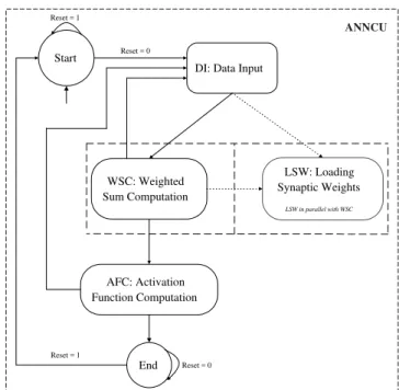
Control Unit: ANNCU
A general view of the control unit ANNCU is depicted in Figure 13. Processing an application neural network starts by obtaining the required data via the control block DI. The fi-nite state machine (FSM) within this block is responsible for
requesting to component LCS the inputsxiof the net. These
data are then stored into specific registers in ANNALU. The state machine within block WSC controls the computation of the weighted sum through fraction sums and products using the provided components in the neuron hardware described earlier.
Once the weighted sum yielded, the state machine within block AFC initiates the control of the same components available in the hardware layer so as to compute the activa-tion funcactiva-tions of the neurons. Once this is done, the compu-tation due to the current neuron layer has been achieved. If the current layer is not the last in the net, then the FSM imple-mented in block AFC sends the control to that impleimple-mented by block DI to iterate the process once more. Otherwise, the output results are ready and therefore, the control unit enters
stateEndand waits for a reset trigger.
LSW: Loading Synaptic Weights
LSW in parallel with WSC WSC: Weighted
Sum Computation
End
Reset = 0
ANNCU
Reset = 0 Reset = 1
Start
DI: Data Input
AFC: Activation Function Computation
Reset = 1
Figure 13: Control flow within ANNCU
As shown in Figure 13, the control unit ANNCU includes two FSMs: primary and secondary. The primary FSM
con-sist of blocks DI, WSC, AFC as well as statesstartandEnd.
The secondary FSM is defined solely by the control within block LSW. which is responsible for preparing the synap-tic weights for the next layer, if any, while and in parallel with the computation of the weighted sums due to the current layer. The current layer synaptic weights are stored in reg-isters within the neuron hardware, allowing for the kind of parallelism. (Details of the FSMs description can be found in (Martins, 1996). These were not included here as this kind of detailed description is not necessary for understanding the overall behavior of the control unit.)
5.3
Clock generator
The macro architecture of Figure 8 include a clock generator, which yields two signal Clk1 and Clk2. Both these signals implement the synchronization of the general activities of the ANNCH, which also interferes in both included units: AN-NALU and ANNCU. The time diagram of the clock signals is shown in Figure 14.
Component ANNCU consists mainly of a state machine the controls the operations performed by ANNALU. The state transitions in this machine occur during the positive
transi-tions of clock signal Clk1. The time period tH1 is the
op-Clk1
Clk2
tH1 tL1 = 3tH1
tH2 = tL2
Figure 14: Clock signals used by the hardware sub-system ANNCH
erates in synchrony with the negative transition fo clock sig-nal Clk2. Note that during one clock cycle with respect to Clk1, four shifting operation may take place. This acceler-ates the the time spent in shifting operations. Shifting opera-tions are required so as to frame the results of addiopera-tions and multiplications within the fractional data representation. The use of faster clock Clk2 is only possible thanks to the reduced time of a shifting operation with respect to that required by the more complex operations performed by ANNALU.
6
PERFORMANCE RESULTS
The architecture is entirely described in VHDL. It was
sim-ulated in ModelSim XE 6.3c. The detailed VHDL code
can be found in (Martins, 1996). Simulation snapshots
accompanied by detailed explanations of the computations done throughout a layer of the ANN hardware are given in (Martins, 1996).
The VHDL specification of the ANN proposed hardware was synthesized for the Xilinx Virtex-5 XC5VFX70T FPGA, through Xilinx XST Synthesis tool (ISE Design Suite 11.1). This synthesis tools allows for integration of soft-ware/hardware co-designs. The ANN hardware sub-system was implemented through automatic synthesis and the soft-ware sub-system was implemented in C language and exe-cuted by a MicroBlaze processor. The MicroBlaze (Xilinx,
2008) is a RISC microprocessor IP from XilinxTM, which
can be synthesized in reconfigurable devices. Although we had access to an embedded PowerPC core, only the MicroB-laze offers a low latency point-to-point communication link,
known as Fast Simplex Link (FSL) (Xilinx, 2009), which
allows the connection of a component, identified as co-processor, to the microprocessor. Therefore, the MicroBlaze is connected to the ANN hardware co-processor through an FSL channel and provides the necessary input data, as shown in Figure 15. The C program, executed by the microBlaze, provides the parameter and coefficient settings for the LCS
three memories via thefrom-microBlazeFSL FIFO, then
af-ter a while receives the results, which are sent by the
co-processor via theto-microBlazeFSL FIFO. The C program
is also responsible of printing the received results on the
ter-minal via the available UART (Universal Asynchronous
Re-ceiver/Transmitter). The timer is used to measure the number of elapsed cycle during the ANN hardware operation.
UART Timer
ANN Hardware
Fast Simplex Link FSL
Peripheral Local Bus PLB
Figure 15: The MicroBlaze processor connected to the ANN hardware co-processor
In Table 1, we report the hardware area required by a single neuron for different numbers of inputs, as well as that needed to implement to whole network, considering the maximum
number of inputs allowed (imax), the maximum number of
neuron per layer (nmax) and the maximum number of
lay-ers (lmax). The required area is given in terms of slices.
Virtex-5 FPGA slices are organized differently from previ-ous generations. Each Virtex-5 FPGA slice contains four 6-input lookup tables and four flip-flops. We compare these figures to those imposed by the binary-radix straightforward design and the stochastic computing-based design (Nedjah and Mourelle, 2007) and a previous MAC-based design, re-ported in (Nedjah et al., 2009).
The used FPGA has 11,200 slices. Therefore, a rough ap-proximations, given the data presented in Table 1, we can expect possible implementations of ANNs of a hundreds of neurons per layer for virtually infinite number of layers. However, only the actual mapping of the hardware with such number of neurons would provide exact figures, as the re-quired area depends on the how the synthesis tool would
op-timize the hardware resources via sharingvs.duplication.
In Table 2, we show the net delay imposed in compari-son with those imposed by the implementations reported in (Nedjah and Mourelle, 2007) and (Nedjah et al., 2009).
From the performance results given in Table 1 and Table 2, it can be observed that in the proposed architecture both the area and computation time are reduced and so the
perfor-mance factor, which is defined as area×1time, was improved,
Table 1: Area requirements of one neuron and network for different number of inputs and net size
imax nmax lmax Neuron area (#Slices) Net area (#Slices)
BIN1 STO2 MAC3 FFP4 BIN1 STO2 MAC3 FFP4
2 6 3 116 8 4 6 98 21 8 11
4 9 5 212 12 8 9 574 75 25 41
8 13 7 436 20 11 15 780 421 57 129
1Binary-radix based (Nedjah and Mourelle, 2007) 2Stochastic (Nedjah and Mourelle, 2007) 3MAC-based floating-point (Nedjah et al., 2009) 4Fraction-based proposed
Table 2: Time delay of a network and performance factor for different number of inputs and net size
imax nmax lmax Net delay (ns) Performance factor (×10
−3)
BIN1 STO2 MAC3 FFP4 BIN1 STO2 MAC3 FFP4
2 6 3 3.45 5.85 3.67 3.33 2.498751 21.3675 68.1198 53.2481
4 9 5 4.92 7.09 5.11 4.71 0.958736 11.7536 24.461 28.1293
8 13 7 11.32 19.87 11.79 9.05 0.202613 2.5163 8.4817 13.3779
1Binary-radix based (Nedjah and Mourelle, 2007) 2Stochastic (Nedjah and Mourelle, 2007) 3MAC-based floating-point (Nedjah et al., 2009) 4Fraction-based proposed
Figure 16: Comparison of the performance factor yield by the neural network hardware proposed here and those reported in the literature
For a testbed application, we use the MLP that implements word recognition of a given speech. The neural network re-quires 220 data as input nodes and returns 10 results as out-put nodes. The network inout-put consists of 10 vectors of 22 components obtained after preprocessing the speech signal. The output nodes correspond to 10 recognizable words ex-tracted from a multi-speaker database (Waibel et. al., 1989). After testing different architectures (Canas, et al., 2003), the best classification results, which achieved a 96.83% of cor-rect classification rate in a speaker-independent scheme, have
been yielded using 24 nodes in a single hidden layer, with full feed forward connectivity. Thus the MLP has two layers of 24 and 10 neurons respectively, as shown in Figure 17, which was taken from (Canas, et al., 2008).
The FPGA implementation of the MLP of Figure 17 has been first used in (Canas, et al., 2008), wherein the activation func-tion is implemented using lookup table after discretizafunc-tion and the handled data are all of 8 bits. Three alternative ar-chitectures has been investigated based on how the required memories that store the input data, the weights and biases as well as the lookup tables used to implement the activation functions are implemented. The implementation alternatives are: distributed memory blocks (DRAM) or embedded mem-ory blocks (BRAM). In the former, the flip-flops available within the configurable logic blocks (CLBs) are used while in the latter specific blocks of RAM are used. Note that, in general, the delay due to the memory access of DRAM blocks is much shorter than that due to BRAM.
Figure 17: Testbed application MLP
the remaining data are stored in DRAM; in alternative (c), BRAMs are used to implement all required memories. In this testbed MLP, input data memory requires a total of 220 en-tries, the weight and biases memory needs to accommodate
220×24 + 24×10 = 5520words and the activation function table, which in our case requires only 9 fractions. However, in the implementation reported in (Canas, et al., 2008), this memory requires much more that this. The authors did not specify how many entries they used to digitize the sigmoid activation function. It is worthwhile noting that a memory entry in our design is of 32 bits while in (Canas, et al., 2008), it is of 8 bits only. Also, the design of (Canas, et al., 2008) was mapped using Virtex-E 2000 FPGA device is used. This family of FPGAs is based on 4-input LUTs.
The chart of Figure 18 illustrate the comparison of the per-formance factor achieved by the proposed design and that obtained for the design using lookup table for the activation function, as reported in (Canas, et al., 2008). The chart shows that our design always wins, i.e. with respect to the investi-gated alternatives for the implementation of the data memo-ries. Our design always requires less hardware area due to re-use of circuitry by both weighted sum and activation function computation. Furthermore, despite the fact that the proposed design requires mores clock cycles to complete the needed computation, it does so at a higher operation frequency.
0 2 4 6 8 10
performance factor
(a) (b) (c)
memory alternatives
Canas Proposed
Figure 18: Comparison of the performance factor for the testbed application
7
CONCLUSIONS
In this paper, we presented a novel hardware architecture for processing an artificial neural network, whose topology
con-figuration can be changedon-the-flywithout any extra effort.
An extra effort was undertaken to implement efficiently arith-metic and computing models. Furthermore, the model mini-mizes the required the silicon area as it uses a single physical layer and re-uses by feedback it to perform all the compu-tation executed by all the layers of the net. This is done so without deteriorating the neural network inference time. The IEEE Standard for Floating-Point Arithmetic (IEEE-754) was not used. Instead, the search for simple arithmetic circuits and which require less silicon area motivated the use of fractions to represent real numbers.
The model was specified in VHDL, simulated to validate its functionality. We also synthesized the system to evaluate time and area requirements. The comparison of the perfor-mance result of the proposed design was then compared to three similar implementations: the binary-radix straightfor-ward design, the stochastic computing based design and the MAC-based implementation with floating-point operations. Furthermore, the design performance was compared to a sim-ilar one that uses a look-up table to implement the activation function. The proposed design has been proven superior in many aspects.
Table 3: Performance comparison of the proposed design with a design that uses a lookup table as activation function
MLP Design Alternative #Slices #BRAM Clock (ns) #Cycles Time (ms) Performance factor
(Canas, et al., 2008)
(a) 6321 0 58.162
282
16.402 2.59
(b) 4411 24 59.774 16.856 4.73
(c) 4270 36 64.838 18.284 3.80
Proposed
(a) 3712 0 49.341
356
17.565 6.05
(b) 2988 13 51.003 18.157 4.25
(c) 2192 20 54.677 19.465 8.80
THANKS
We are grateful to FAPERJ (Fundação de Amparo á Pesquisa
do Estado do Rio de Janeiro,http://www.faperj.br)
and CNPq (Conselho Nacional de Desenvolvimento
Cientí-fico e Tecnológico,http://www.cnpq.br) for their
con-tinuous financial support. We are also thankful to the review-ers whose critics and suggestions improved the paper greatly.
REFERENCES
Bade, S. L. and Hutchings, B. L. (1994). PGA-Based
Stochastic Neural Networks, in IEEE Workshop on FP-GAs for Custom Computing Machines, pp. 189–198, IEEE, Los Alamitos.
Beuchat, J.-L. and Haenni, J.-O. and Sanchez, E.
(1998). Hardware Reconfigurable Neural Networks,
5th. Reconfigurable Architectures Workshop, Orlando, Florida.
Botros, N. M. and Abdul-Aziz, M. (1994).Hardware
Imple-mentation of an Artificial Neural Network using Field Programmable Arrays, IEEE Transactions on Industrial Electronics, vol. 41, pp. 665–667.
Canas, A., Ortigosa, E. M., Diaz, A. F. and Ortega J. (2003).
XMLP: a Feed-Forward Neural Network with Two-Dimensional Layers and Partial Connectivity, Lecture Notes in Computer Science, LNCS, vol. 2687, pp. 89– 96.
Canas, A., Ortigosa, E. M., Ros, E. and Ortigosa, P. M.
(2008). FPGA implementation of a fully and partially
connected MLP — Application to automatic speech recognition, In: FPGA Implementations of Neural Net-works, A. R. Omondi, J. C. Rajapakse (Eds.), Springer.
Chen, C. (2003).Fuzzy logic and neural network handbook,
McGraw-Hill, New York.
Choi, Y. K. Ahn, K.H. and Lee, S.-Y. (1996). Effects of
multiplier output offsets on on-chip learning for ana-log neuro-chips, Neural Processing Letters, vol. 4, pp. 1–8.
Dias, F. M., Antunes, A. and Mota, A. M. (2004). Artificial
neural networks: a review of commercial hardware, Engineering Applications of Artificial Intelligence, Vol. 17, No. 8, pp. 945–952.
Ferrucci, A. T. (1994). A Field Programmable Gate Array
Implementation of self adapting and Scalable Connec-tionist Network, Ph.D. thesis, University of California, Santa Cruz, California.
Gadea, R. Ballester, F. Mocholí, A. and Cerdá, J. (2000).
Artificial Neural Network Implementation on a Single FPGA of a Pipelined On-Line Backpropagation, in Pro-ceedings of the 13th International Symposium on Sys-tem Synthesis, IEEE, Los Alamitos.
Haykin, S. (1999). Neural Networks: A Comprehensive
Foundation, Second Edition, Prentice Hall Interna-tional, New Jersey.
Holt, J. L. and Baker, T. E. (1991). Backpropagation
simula-tions using limited precision calculasimula-tions, In: Proceed-ings, International Joint Conference on Neural Net-works, vol. 2, pp. 121–126.
Kung, H. T. (1988). How We got 17 million connections
per second, in International Conference on Neural Net-works, vol. 2, pp. 143–150.
Kung, S. Y. (1988). Parallel architectures for artificial
neu-ral networks, In International Conference on Systolic Arrays, pp. 163–174, 1988.
Kung, S. Y. and Hwang, J. N. (1989). A Unified Systolic
Architecture for Artificial Neural Networks, Journal of Parallel Distributed Computing, vol. 6, pp. 358–387.
Linde, A., Nordstrom, T. and Taveniku, M. (1992). Using
FPGAs to implement a Reconfigurable Highly Paral-lel Computer, In Selected papers from: Second Inter-national Workshop on Field Programmable Logic and Applications, pp. 199–210, Springer-Verlag, Berlin.
Lindsey, C. S. and Lindblad, T. (1994). Review of hardware
on Neural Networks: From Biology to High Energy Physics.
Martins, R. S. (2010).Implementação em hardware de redes
neurais artificiais com topologia configurável, M.Sc. Dissertation, Post-graduate Program of Electronics En-gineering, State University of Rio de Janeiro – UERJ, UERJ/REDE SIRIUS/CTCB/S586, 2010.
Martins, R. S., Nedjah, N. and Mourelle, L. M. (2009). Reconfigurable MAC-based architecture for parallel hardware implementation on fpgas of artificial neu-ral networks using fractional fixed point
representa-tion, Procs. of ICANN09, LNCS 5164, pp. 475–484,
Springer, Berlin.
Moerland, P. D. and Fiesler, E. (1997). Neural Network
Adaptations to Hardware Implementations, in Hand-book of Neural Computation, Oxford University Pub-lishing, New York.
Montalvo, A. Gyurcsik, R. and Paulos, J. (1997). Towards a
general-purpose analog VLSI neural network with on-chip learning, IEEE Trans. on Neural Networks, vol. 8, no. 2, pp. 413–423.
Nedjah, N. and Mourelle, L. M. (2007). Reconfigurable
hardware for neural networks: binary versus stochastic, Journal of Neural Computing and Applications, Vol. 72, No. 12, pp. 249–155. Springer, London.
Nedjah, N., Martins, R. S., Mourelle, L. M. and Carvalho, M. V. S.(2008). Reconfigurable MAC-based architec-ture for parallel hardware implementation on FPGAs of
artificial neural networks, Procs. of ICANN08, LNCS
5768, pp. 169–178, Springer, Berlin.
Nedjah, N., Martins, R. S., Mourelle, L. M. and Carvalho, M. V. S. (2009). Dynamic MAC-based architecture of artificial neural networks suitable for hardware imple-mentation on FPGAs, Neurocomputing, Vol. 72, No. 10–12, pp. 2171–2179, Elsevier, Amsterdam.
Nedjah, N., Martins, R. S., and Mourelle, L. M. (2011).
Ana-log Hardware Implementations of Artificial Neural Net-works, Journal of Circuits, Systems, and Computers, vol. 20, no. 3, pp. 349–373.
Santi-Jones, P. and Gu, D. (2008). Fractional fixed point neu-ral networks: an introduction, Department of Computer Science, University of Essex, UK.
Tanenbaum, A. S. (2007).Structured computer organization,
5th. Edition, Prentice Hall PTR, New Jersey.
Uyemura, J. P. (2002).Introduction to VLSI circuits and
sys-tems, 10th. Edition, Wiley, New York.
Rojas, R. (1996). Neural networks, Springer-Verlag, Berlin.
Omondi, R. , Rajapakse, J. C. (2008).FPGA implementation
neural networks, Springer, Berlin.
Waibel, A., Hanazawa, T., Hinton, G., Shikano, K. and
Lang K. (1989). Phoneme Recognition Using
Time-Delay Neural Networks, IEEE Transactions on Acous-tics, Speech, and Signal Processing, vol. 37, no. 3, pp. 328–339.
Wolf, W. (2004). FPGA-based system design, Prentice Hall
PTR, New Jersey.
Xilinx, (2008). Microblaze processor reference guide,
http://www.xilinx.com/support/
documentation/ sw\_manuals/mb\_ref\ _guide.pdf, last acess: April, 2011.
Xilinx, (2009). Fast simplex link v2.11b, http://www.
xilinx.com/support/documentation/ip \_documentation/ fsl\_v20.pdf, last access: April, 2011.
Zhang, X. and et al.,(1990). An Efficient Implementation of
the Back propagation Algorithm on the Connection Ma-chine, Advances in Neural Information Processing Sys-tems, vol. 2, pp. 801–809.
Zhang, D. and Pal, S. K. (1992). Neural Networks and
Sys-tolic Array Design, World Scientific Company, Singa-pore.
Zhu, J. and Sutton, P. (2003). FPGA Implementations of
neural networks – A survey of a decade of progress, In: Field Programmable Logic and Application, Lec-ture Notes in Computer Science, Vol. 2778, pp. 1062– 1066, Springer, Berlin.
Zurada, J. M. (1992). Introduction to artificial neural