Hot Electron Transport Properties in Characteristics of Wurtzite GaN MESFETs Using a
Five-valley Model
H. Arabshahi∗ and M. Rezaee Rokn-Abadi
Department of Physics, Ferdowsi University of Mashhad, Mashhad, Iran (Received on 24 November, 2008)
Ensemble Monte Carlo simulations have been carried out to investigate the effects of upper valleys on the characteristics of wurtzite GaN MESFETs. Electronic states within the conduction band valleys at theΓ1,U, M,Γ3andKare represented by non-parabolic ellipsoidal valleys centred on important symmetry points of the
Brillouin zone. The following scattering mechanisims, i.e, impurity, polar optical phonon, acoustic phonon, alloy and piezoelectric are inculded in the calculation. Ionized imurity scattering has been treated beyound the Born approximation using the phase-shift analysis. The simulation results show that on the drain side of the gate region, hot electrons attained enough energy to be scattered into the upper satellite conduction valleys. Approximately %20 of the electrons occupy the higher valleys (mainlyUandMvalley). The simulated device geometries and doping are matched to the nominal parameters described for the experimental structures as closely as possible, and the predicted drain current and other electrical characteristics for the simulated device including upper valleys show much closer agreement with the available experimantal data.
Keywords: Monte Carlo; Ellipsoidal valleys; Ionized impurity; Phase-shift
1. INTRODUCTION
GaN has become an attractive material for power transis-tors due to its wide band gap, high breakdown electric field strength, and high thermal conductivity [1-3]. Also the ma-terial has a relatively high electron saturation drift velocity and low relative permittivity, implying potential for high fre-quency performance [4-5]. Due to its wide band gap, GaN is a primary candidate for optoelectronic devices operating with blue to ultraviolet wavelengths and electronic devices operating at high temperatures and high power levels [6]. Several GaN-based transistors, superlattices, and quantum well devices intended for both electronic and optoelectronic applications [7-8]. Improved electron transport properties are one of the main targets in the ongoing study of GaN material and devices. It is considered reasonably well es-tablished that the electron drift velocity dependence on elec-tric field has a region of negative differential conductivity. The electron drift velocity is predicted to have a maximum of
∼2.3×10⁵ms−1at∼2×10⁷Vm−1forT=300 K and with an impurity concentration of about 1022m−3[9]. The velocity-electric field dependence exhibits remarkable thermal stabil-ity between 300 and 600 K.
In this work an ensemble Monte Carlo calculations of steady state electron transport in wurtzite GaN based field effect transistor has been presented. In next section, details of the device fabrication and simulation model which is used in the characteristic of the device are presented. Details of the effects of upper valley in GaN MESFETs and the results obtained are interpreted in section 3.
2. MODEL, DEVICE AND SIMULATIONS
An ensamble Monte Carlo simulation have been carried out to simulate the electron transport properties in wurtzite
∗Electronic address:[email protected]
GaN MESFET. The method simulate the motion of charge carriers through the device by following the progress of 104 superparticles. These particles are propagated classically be-tween collisions according to thier velocity, effective mass and the prevailing field. The selection of the propagation time, scattering mechanism and other related quantities is achieved by generating random numbers and using this num-bers to select, for example, a scattering mechanism. Our self-consistent Monte Carlo simulation was performed us-ing an analytical band structure model consistus-ing of five non-parabolic ellipsoidal valleys. The pseudopotential band structure shows the conduction band minimum to be located at theΓpoint (Γ1), and lowest energy conduction band satel-lite valleys to occur at theUpoint (located about two thirds of the way between theLandM symmetry points). Higher conduction band valleys are located at theΓpoint (Γ3), at the
Mpoint, and at theKpoint (figure 1).
In our Monte Carlo simulation, the two differentΓvalleys, the six equivalentU valleys, the three equivalentM valleys and the two equivalentK valleys are represented by ellip-soidal, non-parabolic dispersion relationships of the follow-ing form [10-11]
E(k)[1+αiE(k)] =
~2
2
"
k2 x+k2y
m∗⊥ + kz2 m∗k
#
(1)
wherem∗⊥andm∗kare the transverse and longitudinal effec-tive masses at the band edge andαi is the non-parabolicity
A L M Γ A H K Γ
Wavevector (K)
3.5 5.5 7.5 9.5 11.5
Energy (eV)
WZ GaN
U
M K
Γ3
Γ1
0.0 3.0 4.0 6.0 8.0
FIG. 1: Five-valley model of the two lowest conduction bands of wurtzite GaN used in the Monte Carlo simulations.
Electron particles in the ensemble Monte Carlo simulation occupy non-parabolic ellipsoidal valleys in reciprocal space, and obey Boltzmann statistics. Herring-vogt transformations are used to map carrier momenta into spherical valleys when particles are drifted or scattered. The electric field equations are solved self-consistently with the electron transport us-ing a finite difference method, and the device grid potentials are updated at each ensemble drift timestep (1 femtosecond). The geometry of the device to be simulated is specified at the beginning of the simulation by defining it in anx−yplane as a set of joined rectangular regions, each with uniform doping and other material parameters, and a set of contact regions. All physical quantities are assumed constant in thez direc-tion (device width).
Figure 2 shows a simple example of joined rectangular re-gions and contacts for a MESFET structure. The solution of Poisson’s equation is based on a finite difference method which requires that all the rectangular regions of the device are divided into uniform arrays of two-dimensional mesh cells. The cells may differ in form from region to region but it is necessary that they match in size along the join between two adjacent regions.
0.00000 5000.00000 10000.00000 15000.00000 0.00000
00.00000 00.00000 00.00000 00.00000
Drain Gate
Source
∆
x y
X Y
∆
FIG. 2: Device geometry and discretization of a MESFET. There are three regions and three contacts S, G and D. The mesh cells are uniform within any single region and match at the joins.
In figure 2 the rectangular source and drain regions have identical uniform mesh cells which are different from those
0.0 0.5 1.0
0.0 0.5 1.0
e
X Y
Pij
∆x
∆y
φij
Eij y
Eij x
Ei,j+1 y
Ei+1,j x
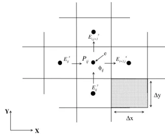
FIG. 3: Nearest-grid-point method for charge assignment in two-dimensions. The charge density at a mesh pointPi j is taken to be
the total charge in the mesh cell surrounding the mesh pointPi j
divided by the cell area. Note discretized electric fieldEi jand
elec-tric potentialφi j, (E=−∇φ) are used in the solution of Poisson’s
equation.
in gate region, but match at the joins. The cells also form the frame of reference in which the particles move under the influence of the electric field. The definition of the mesh (shape and size of the cells) is dependent on the details of the device and the simulation, since, for example, the resolution of the electric field is limited by the size of the mesh cells.
The simplest method for assigning charged particles to cells is the nearest-grid-point scheme in which the total charge found in a cell is assigned to the midpoint of that cell (figure 3). After each sampling Poisson’s equation is solved and the electric field is updated. Poisson’s equation is solved by a combined fast Fourier transform [12-13] and Buneman cyclic reduction method [14] developed by Walm-sley and Abram [15]. This calculational scheme is integrated with a capacity matrix approach [16] that facilitates the use of individual rectangular regions to form more complicated structures.
After setting all the material and device parameters, the simulation is started in a state of charge neutrality every-where in the device. The simulated particles are distributed appropriately among all the mesh cells to achieve the re-quired neutrality. In the two-dimensional device models used here there is no variation of electron density or electric field normal to thex−yplane and scaler quantities at a timestep like electron density, energy and potential are located at the center of the cells, whereas vectorial quantities like the elec-tric field components or the velocity components are always calculated first at midpoint between the scaler quantities.
The particles that leave cell (i,j) inx-direction enter cell (i+1,j) and analogously for they-direction. Therefore, the total number of electrons in the simulated transistor can only be changed at the boundary of the simulation regions.
repere-0.0 0.5
1.0 2.3 µm
0.5 µ
m
0.5 µm
0.5 µm
Doped GaN active layer
GaN buffer layer
0.15 µm
0.35 µm
Source & Drain = Ohmic Contacts
Gate = Schottky Contact
(I)
(II)
(I)
(II)
5*1023 m−3
2*1023 m−3
1*1022 m−3
0.3 µm
0.8 µm 1.2 µm
FIG. 4: Cross section of wurtzite GaN MESFET structure which we have chosen in our simulation. Source and drain contacts have low resistance ohmic contacts, while the gate contact forms a Schottky barrier between the metal and the semiconductor epilayer.
sent the contact potential at the Au/Pt. The source and drain regions are doped to 5×10²³ m−3 and the top and down buffer layers are doped to 2×10²³ m−3and 1×10²² m−3, respectively. The effective source to gate and gate to darin separation are 0.8 µm and 1.2µm, respectively. The large dimentions of the device need to a long simulation times to ensure convergence of the simulator.
3. RESULTS
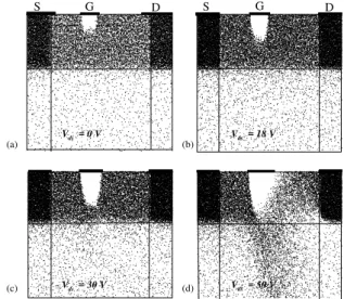
Figure 5 compares the instantaneous distribution of elec-trons throughout the device in the steady-state for different gate and drain biases at room temperature. When a posi-tive potentialVdsis applied to the drain, electrons flow from
source to drain, giving a currentIdsfrom source to drain. The
depletion region of the Schottky barrier restricts the current path to the lower part of the channel and the buffer layer. At zero drain bias (figure 5a), the depletion layer beneath the gate has a symmetric shape. At zero gate and drain bias, the depletion region corresponds to that associated with the built-in potential of the Schottky barrier, but is larger for the case of gate biasVgs=−1 V shown here. AsVdsis increased
from zero, the depletion layer becomes asymmetric in shape since the potential difference between the gate and the chan-nel is greater at the drain end than the source end of the gate. The channel is more constricted at the drain end of the gate (see for example atVd=18 and 30 volt in figures 5b and 5c)
and the field along the channel is also higher in that region. As the drain-source voltage is increased still further, the field at the drain end of the gate approaches the value at which the electron velocity along the channel saturates. Be-yond this value, which corresponds to the threshold voltage in the drain current-voltage characteristics, further increase in drain-source voltage does not substantially increase the drain-source current. The length of the region of the chan-nel over which the electrons are in velocity saturation in-creases and there is some carrier accumulation within the channel. The depletion layer edge at the drain end of the gate also moves closer to the drain as the drain-source
volt-0 5e+03 1e+04 2e+04
0 5e+02 1e+03 2e+03 2e+03 (a)
Vds = 30 V
V
ds = 18 V
Vds = 50 V
V
ds = 0 V
S G D
S G D
(b)
(c) (d)
FIG. 5: Depletion layer profiles for different drain and gate biases for GaN MESFET at room temperature.
age increases. Note also that the transition between the gate depletion region and the charge neutral bulk is far from sharp on the drain side. At a sufficiently negative gate potential the depletion layer punches through to the high-resistivity buffer layer, and the source and drain electrodes are connected only by leakage paths within the buffer layer and substrate (see figure 5d).
An important factor in the high frequency performance of the MESFET is the time taken for electrons to traverse the region of the device beneath the gate, and the performance is enhanced by a high average electron velocity through that region.
The spatial distribution of hot electrons throughout the de-vice for each valley atVgs=−1 V andVds=50 V for room
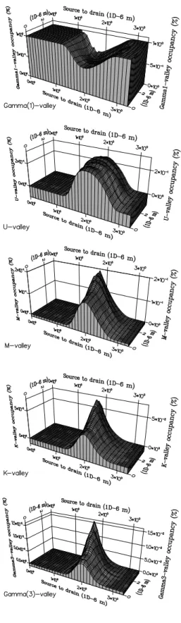
temperature operation is shown in figure 6. Electrons are seen to exist in the upper valleys only to the right of the high field region, which exists on the drain side of the gate, be-cause it is only there that the electrons have attained enough energy to be scattered into the satellite conduction valleys. Also note there is an injection of electrons from the channel into the buffer layer; a process which is eventually opposed by the electric field created by the resulting negative space charge in the buffer layer. Figure 6 also shows that the dis-tribution of electrons occupying the upper valleys extends a significant way towards the drain region where the elec-tric field is much lower. This is a result of the finite time that it takes for phonon scattering to return the electrons to theΓ-valley. Figure 7 shows the valley electron occupancies throughout the device. It can be seen that significant electron transfer to the upper valleys only begins to occur under the gate. Approximately 20% of the electrons occupy the higher valleys (mainlyU andMvalleys) in the vicinity of the gate which is similar to the valley occupancy ratio in the active layer of the n+-n-n+diode.
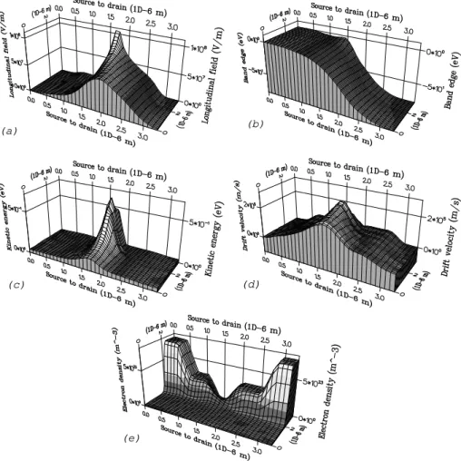
Figure 8 shows various microscopic properties of the de-vice when the source-drain bias is 50 V and the gate volt-age is -1 V; specifically the longitudinal electric field, the
Γ valley electrons
S G D
Vds= 50 V Vgs= −1 V (a)
U valley electrons
Vds= 50 V
Vgs= −1 V
(b)
M valley electrons K valley electrons
Vds= 50 V Vgs= −1 V
(c)
FIG. 6: The distribution of hot electrons at room temperature for Vgs=−1 V,Vds=50 V in centralΓvalley and upper valleys.
of distance from the source. The longitudinal electric field plotted in figure 8a shows the high electric field in the region under the gate, which has been referred to earlier. Related to this is theΓ-valley band profile throughout the device in fig-ure 8b. Note almost all the drain-source potential is dropped within the gate-drain region, leaving a flat potential profile near the source and drain. As electrons move towards the drain, they lose potential energy and gain sufficient kinetic energy to transfer to the upper conduction valleys where their drift velocity is reduced. The variations of average electron kinetic energy and average drift velocity throughout the sim-ulated device are shown in figures 8c and 8d, respectively. The average electron velocity reaches about 2.1×10
5ms−1 and then declines towards the drain. The steep decrease in the average kinetic energy on the drain side of the gate is due to the transfer of electrons to the upper valleys. The electron density through the device is shown in figure 8e. The gate depletion region is clearly seen where the electron density is several orders of magnitude lower than it is near the source and drain.
The drain current is obtained by counting the net charge flow through the drain contact. Figures 9a and 9b show the
FIG. 7: The valley occupation ratios for the centralΓ1-valley and
(a)
(a) (b)(b)
(c)
(c) (d)(d)
(e) (e)
FIG. 8: Three dimensional distribution of electron data recorded through the simulation of the GaN MESFET when the source-drain bias is 50 V and the gate voltage is−1 V at room temperature. This figure shows: (a) Longitudinal electric field, (b)Γ-valley conduction band profile, (c) Average kinetic energy, (d) Drift velocity and (e) Electron density.
calculated drain current versus drain-source voltage at differ-ent gate biases for temperatures of 300 K and 420 K. Figure 9c shows the experimental results for the same device ob-tained by Trassaertet al.[17] at 300 K and a further presen-tation of the simulation results to facilitate comparison. The simulated characteristics at 300 K show good saturation be-haviour with a knee voltage around 20-30 V and a saturation drain current of about 2200 mA mm−1forVgs=0 V. The
high drain current density is encouraging for the use of GaN for high-power applications.
Figure 9c shows the the simulatedI-Vcharacteristics is in fair agreement to the experimental measurements.
From figure 9a it is clear that the device is not completely pinched-off even at large negative gate bias (Vgs=−15 V)
which is due to strong electron injection into the buffer layer at high electric fields. An increasing fraction of the drain cur-rent flows through the buffer as the drain voltage increases. AtVds=80 V essentially the whole drain current flows
en-tirely through the buffer. To obtain some idea of the effect of high temperature on GaN MESFETs, simulations were carried out atT =420 K, keeping the other device parame-ters unchanged. TheI-Vcurves obtained are shown in figure 5.7b. Comparing theI-Vcurves atT=300 and 420 K, it can be seen that the drain current is somewhat lower at the higher
temperature, due to increased phonon scattering, but the ef-fect is not major. The transconductance of the MESFET is given by
gm=
∆Id
∆Vg Vd
(2)
and is calculated from figure 9a to be about 140 mS mm−1 at 18 V drain bias and−1 V gate voltage for room temper-ature. When the drain bias is increased to 50 V at the same gate voltage, the transconductance increases approximately to 200 mS mm−1. In comparison, good GaAs MESFETs without a gate recess have a transconductance around 110 mS mm−1[18-19]. The higher value of transconductance in simulated GaN MESFET is related to a higher drain current.
Conclusions
0.0 20.0 40.0 60.0 80.0 100.0 Drain−source voltage, Vds(V)
0.0 500.0 1000.0 1500.0 2000.0 2500.0
Drain current, I
d
(mA/mm)
0.0 V −1.0 V
−3.0 V
−5.0 V −7.0 V −9.0 V
−11.0 V −13.0 V −15.0 V
T = 300 K (a)
0.0 20.0 40.0 60.0 80.0 100.0 Drain−source voltage, Vds(V)
0.0 500.0 1000.0 1500.0 2000.0 2500.0
Drain current, I
d
(mA/mm)
0.0 V −1.0 V −3.0 V −5.0 V −7.0 V −9.0 V −11.0 V −13.0 V −15.0 V
T = 420 K (b)
0.0 10.0 20.0 Drain−source voltage, Vds(V) 0.0
1000.0 2000.0 3000.0
Drain current, I
d
(mA/mm)
0.0 10.0 20.0 Drain−source voltage, Vds(V) 0.0
200.0 400.0 600.0
Drain current, I
d
(mA/mm)
+1
−1 −3 −5 −7 −9
+1
−1
−3
−5
−7
−9
Experimental results
T = 300 K
Simulation results
T = 300 K
(c)
0.0 500.0 1000.0 1500.0
FIG. 9: (a) The simulated drain current versus drain voltage atT=300 K, (b) The simulated drain current versus drain voltage atT =420 K and (c) Comparison of the experimentalI-Vcharacteristics for the same device atT=300 K with the simulated device.
will produce a serious reduction in the drain current and con-sequently the output power of GaN MESFET. Also the high output darin currents of the simulated device shows GaN is a good candidate for high-power and high-temperature appli-cations.
Acknowledgments
I would like to thank Maryam Gholvani for writing up the paper.
[1] R. J. Trew, M. W. Shin and V. Gatto,Solid-State Electronics.
411561 (1997)
[2] E. R. Brown,Solid-State Electron.422119 (1998)
[3] K. Shenai, R. S. Scott and B. J. Baliga,IEEE Trans. Electron Devices.361811 (1989)
[4] S. Strite and H. Morkoc,J. Vac. Sci. Technol.B101237 (1992) [5] J. D. Albrecht, R. P. Wang and P. P. RudenJ. Appl. Phys.83
4777 (1998)
[6] L. F. Eastman, K. Chu, J. Smart and J. R. Shealy,Mater. Res. Soc. Symp. Proc.5123 (1998)
[9] H. Arabshahi and M. H. Ghasemian,Modern Physics Letters B.221397 (2006)
[8] M. A. Khan and J. W. Yang,Appl. Phys. Lett.763807 (2000) [9] H. Arabshahi,Modern Physics Letters B.21199 (2007) [18] C. Moglestue,Monte Carlo simulation of semiconductor
de-vices, Chapman and Hall (1993)
[11] B. K. Ridley,Electrons and phonons in semiconductor multi-layers, Cambridge University press (1997)
[12] J. W. Cooley and J. W. Tukey,Mathematics of Computation.
19, 297, (1965)
[14] G. D. Bergland,Mathematics of Computation.21, 236, (1967) [14] G. D. Bergland,Mathematics of Computation.22, 275, (1968) [15] M. Walmsley and R. A. Abram,The international Journal for
Computation and Mathematics.15, 31, (1996)
[16] C. Temperton, Journal of Computational Physics. 34, 314, (1980)
[17] S. Trassaert, B. Boudart and C. Gaquiere, a1404 ORSAY France 127 (1999)
[18] C. Moglestue,IEEE Proceedings.132, 217, (1985)