Nonlinear Spatio-Temporal Dynamics in Semiconductors
EckehardSchollTechnische Universitat Berlin, Institut fur Theoretische Physik, Hardenbergstr. 36, D-10623 Berlin, Germany
Received 27 May, 1999
We review recent theoretical advances in the modeling and computer simulation of complex non-linear spatio-temporal dynamics of charge carriers in semiconductors. Among the particularly instructive examples are investigations of current laments in doped semiconductors in the regime of low temperature impurity breakdown. The nascence of current laments in thin GaAs lms with dierent contact geometries, including circular samples (Corbino disks) with symmetry breaking instabilities, is investigated, and the role of global couplings induced by the operating load circuit is analysed.
Semiconductors are complex nonlinear dynamic systems which exhibit current instabilities and self-organized formation of spatio-temporal patterns under the inuence of strong electric elds [1, 2, 3, 4, 5]. Within the past years semiconductors have become a convenient model system for the study of such phenom-ena since sophisticated growth technologies and spa-tially and temporally resolved measurement techniques have provided the possibility to investigate semiconduc-tor structures with desired properties. While a descrip-tion of transport in terms of simple reacdescrip-tion-diusion or drift-diusion models is possible for various semi-conductor structures like pnpn-diodes, pin-diodes, or thin-lm structures, some semiconductor systems may require rened modellingin terms of more sophisticated transport models like hydrodynamic balance equations for the carrier densities, mean carrier momenta and mean carrier energies, or even a kinetic approach in terms of the semiclassical Boltzmann equation or a full quantum transport theory [6]. Often a combination of these approaches is used.
Semiconductor transport instabilities are character-ized by a nonlinear dependence of the current density j upon the electric eldE . This relation is often
non-monotonic and displays negative dierential conductiv-ity (NDC). Two important cases are described by an N-shaped or an S-shaped j(E) characteristic, and
de-noted by NNDC and SNDC, respectively. However,
more complicated forms likeZ-shaped, loop-shaped, or
disconnected characteristics are also possible [7]. In case ofNNDC, theNDCbranch is often but not always - depending upon exernal circuit and boundary condi-tions - unstable against the formation of eld domains, while in theSNDCcase current lamentation generally occurs [8]. These primary selforganized spatial patterns may themselves become unstable in secondary bifurca-tions leading to periodically or chaotically breathing, rocking, moving, or spiking laments or domains, or even solid-state turbulence and spatio-temporal chaos. Within the last decade the introduction of concepts and methods from nonlinear dynamics and pattern for-mation has stimulated a large amount of experimen-tal and theoretical work in a variety of semiconducting materials, e.g. p-Ge or n-GaAs at liquid Helium tem-peratures, or layered semiconductor structures likepin, pnpn, double-barrier resonant tunneling or
cen-wards more complexspatio-temporal dynamics includ-ing the dynamics of solitary laments and multilamen-tary states, spatio-temporal chaos, higher bifurcations of the elementary dissipative structures, interaction of defects and structural imperfections with pattern for-mation, and complex two-dimensional sample and con-tact geometries.
In this review some of these concepts will be il-lustrated by the dynamics of current laments in the regime of low-temperature impurity breakdown in n-GaAs where SNDC occurs. S-shaped characteristics and current lamentation have also been observed in heterostructure hot electron diodes [19, 20, 21] and in thyristor-like multilayered Si or GaAs semiconduc-tor structures [22, 23, 24]. Other semiconducsemiconduc-tor sys-tems where nonlinear transport phenomena and pattern formation have been found include parallel transport in modulation{doped heterostructures associated with real-space transfer [25, 26], i.e., the real-space analog of the Gunn eect, and vertical transport in a superlat-tice [27, 28, 29, 30], as well as eld-enhanced trapping in semi-insulating GaAs [31]; in all those systems the current-eld characteristic is N-shaped and leads to the formation of electric eld domains and oscillatory in-stabilities. Nonlinear spatio-temporal carrier dynamics in low-dimensional semiconductor structures like quan-tum wires and quanquan-tum dots has also become an active eld recently [32, 6].
I Simulation of current
la-ments in the impurity
break-down regime
Impact ionization of charge carriers is a key process in inducing instabilites and spatio-temporal structures in semiconductors. It is a process in which a charge carrier with high kinetic energy collides with a sec-ond charge carrier, transferring its kinetic energy to the latter which is hereby lifted to a higher energy level. The result of the process is carrier multiplication which may induce electrical instabilities at suciently high external electric elds. Impact ionization from shallow donors or acceptors is responsible for impurity breakdown at low temperatures where almost all car-riers are bound to shallow impurities. Being a nonlin-ear autocatalytic process, it induces a nonequilibrium phase transition [1] between a low conductivity and a
spatio-temporal instabilities including self{oscillations and chaos as rst observed by Aoki [33] and Teitsworth et al [34]. If a critical threshold voltage is applied to the semiconductor sample, the free carrier concentra-tion grows in an avalanche-like manner, and the current increases by orders of magnitude at an almost constant voltage due to current lamentation and lateral growth of laments.
Current lamentation is usually attributed to the bistability of an S-shaped dependence of the current
density j on the electric eld E, i.e. SNDC. The
spa-tial coexistence of the high-conductivity and the low-conductivity state at a xed voltage leads to the forma-tion of current laments. In generaforma-tion-recombinaforma-tion models [1] the bistability is caused by impact ionization of multilevel impurities. The generation-recombination cycle starts with impact ionization from the ground state and is afterwards sustained by impact ionization of much less strongly bound excited states.
We consider a doped semiconductor at tempera-tures of liquid Helium. In the following we shall as-sume n-type material; p-type semiconductors can be treated analogously. The carrier density in the conduc-tion band, and hence the current density, is determined by the generation-recombination (GR) processes of car-riers between the conduction band and the donor levels. The experimentally observed S-shaped current density-eld relation in the regime of impurity breakdown can be explained in terms of standard GR kinetics only if impact ionization from at least two impurity levels is taken into account [51]. Therefore we model the innite hydrogenlike energy spectrum of the shallow donors by the ground state and an \eective" excited state close to the band edge. In this case the state of the sys-tem can be characterized by the spatial distribution of the carrier densities in the conduction band n(r;t) as
well as in the impurity ground state and excited state
n 1(
r;t), n 2(
r;t), respectively, where r is the position
vector andt denotes time.
In the following we shall adopt an approach which combines Monte Carlo (MC) simulations of the micro-scopic scattering processes and GR kinetics with rate equations for the macroscopic spatio-temporal dynam-ics of the carrier densities which occurs on a much slower time-scale than the microscopic dynamics. First, we will list the macroscopic constitutive equations.
The temporal evolution ofnis governed by the
con-tinuity equation _
n= 1 e
rj+(n;n 1
;n 2
;jEj); (1)
where the dot denotes the partial derivative with re-spect to time, e is the electron charge and E is the
local electric eld within the sample. Within the drift-diusion approximation the current density j can be
expressed as
j=e(nE+D rn) (2)
with the eld-dependent mobilityand diusion
coe-cientD. We assume the validity of the Einstein relation
D =k
B T
L
=e, wherek
B is Boltzmann's constant and T
L is the lattice temperature.
The rateof GR processes depends on the local
val-ues of the carrier densities in the conduction band and at the impurities, given byn, n
1, and n
2, respectively,
and the strength of the electric eld E =jEj.
Analo-gously, rates 1,
2determining the temporal evolution
ofn 1,
n
2 can be dened as
_ n i= i( n;n 1 ;n 2
;E) (3)
withi= 1;2.
In an explicit two-level model [1], e.g., the GR rates are given by
= X S 1 n 2 ,T S 1 np t+ X 1 nn 1+ X 1 nn 2 ; (4) 1 = T n 2 ,X n 1 ,X 1 nn 1 ; (5) 2 = ,, 1 ; (6) wherep t= N D , n 1 , n
2is the density of ionized donors, N
Dis the total density of donors, X
S
1 is the thermal
ion-ization coecient of the excited level,T S
1 is its capture
coecient,X 1,
X
1 are the impact ionization coecients
from the ground and excited level, respectively,X ,
T
denote the transition coecients from the ground level to the excited level and vice versa, respectively.
The electric eld is coupled to the carrier densities via Gauss' law
rE=e(N D ,n 1 ,n 2
,n); (7)
whereis the dielectric constant and N D N D ,N A
holds with the compensating acceptor concentration
N
A. From equations (1),(3),(6),(7) the charge
conser-vation equation can be derived, given byrJ= 0 with J=E_ +j, where J is the total current density
com-posed of displacement current and conduction current densities.
The essential nonlinearities of the constitutive model equations (1)-(7) in the regime of low-temperature impurity breakdown are contained in the dependence of the GR coecients uponn, n
1, n
2, and E. In order to derive these from a microscopic theory
we have performed single particle MC simulations for a spatially homogeneous steady state [44].
The microscopic rates of all band-impurityprocesses depend upon the carrier densities in the band and im-purity states, which in turn depend upon the nonequi-librium carrier distribution function. To obtain these carrier densities, the MC method has to be combined self-consistently with the rate equations (1)-(3) in the homogeneous steady state, where the GR coecients
X 1, X 1, T S
1 are calculated by averaging the microscopic
transition probabilities (P 1 ii, P 2 ii, P
r ec for impact
ion-ization from the ground state, the excited state, and capture, respectively) over the nonequilibrium distri-bution functionf(k), which is extracted from the MC
X1(n;n1;n2;
E) = 1
nn1 Z
d3k f( k;n;n
1;n2; E)P 1 ii( k;n 1); X 1(n;n
1;n2;
E) = 1
nn2 Z
d3k f( k;n;n
1;n2; E)P
2 ii(
k;n
2); (8)
TS 1(n;n
1;n2;
E) = 1
npt Z
d3k f( k;n;n
1;n2; E)P
r ec( k;p
t):
Note that f, and hence X1, X 1 and T
S
1, in turn depend
parametrically on n, n1, n2 and
E. An iteration
proce-dure, where n1 and n2 are expressed by their
steady-state dependence on n andE, is used to solve the above
problem self-consistently [44].
It is possible to express the dependence of the GR coecients uponEand n through the electron
tem-perature Te(
E;n) [46]. Here we use the notion of
elec-tron temperature Tein the usual sense of the mean
elec-tron energy (3=2)kBTe=
hEi= (~ 2=2m)
hk 2
i, i.e. the
electron temperature is extracted from the MC data es-sentially as the second moment of the nonequilibrium distribution function f(k). This should not be
con-fused with the concept of a heated Maxwellian distribu-tion funcdistribu-tion, where the electron temperature appears as a parameter. This latter concept is much more re-strictive since it assumes a quasi-thermal equilibrium of the conduction band subsystem. The MC data yield a strong increase of Te with rising electric eld
on the high-conductivity branch of the current-voltage characteristics as opposed to only a slight increase on the low-conductivity branch. Physically the strong in-crease is associated with a population inversion between the donor ground and the excited state on the upper branch. For E > 9V/cm impact ionization does no
longer contribute to energy relaxation in a signicant way since the donor ground states are almost com-pletely ionized and impact ionization from the excited state dominates, which is now more strongly populated than the ground state. The GR cycle runs now between the donor excited state and the conduction band. Be-cause of the much smallerenergies involved, this process cools less eciently.
In the following sections our strategy will be to in-sert tted analytical representations of the MC data into the macroscopic equations (1)-(7). We use this approach in order to take into account as much de-tailed information as possible about the microscopic
scattering processes, while still retaining manageable expressions. As a check of consistency, the spatially uniform stationary n(E) characteristic which we obtain
with the tting functions from (4)-(6) in the steady state using the condition of charge neutrality N
D =
n(E) + n 1(
E;n) + n 2(
E;n), can be compared with the
characteristic obtained by direct MC simulation. The S-shaped negative dierential conductivity (SNDC) is successfully reproduced.
II Current lament formation
in point contact samples
In this section we shall present exemplary two-dimensional simulations for thin samples with point contacts, considering the longitudinal x-direction as well as the transverse z-direction. In this way it is pos-sible to model the dynamics of current laments. We consider a rectangular sample with side lengths Lx= 5
and Lz = 7:5 mm with two small circular contacts of
diameter 1 mm at a distance of 3.5 mm in x-direction, representing a thin n-GaAs lm with point contacts (thickness 14m). At the contacts n is xed to a value nD= 5
10
15cm,3to model Ohmic contacts. All other
boundaries are treated as insulating where the compo-nents of the current density j and the electric eld E
perpendicular to the boundaries vanish. Our numeri-cal algorithm employs an implicit nite element scheme [52].
We study the nascence of current laments when a bias voltage U0 is applied to the sample in series with
a load resistor R so that the semiconductor is forced from the nearly insulating state to a highly conducting state. Within 1 ps the bias voltage is linearly increased from U0 = 0 to U0 = 20 V. Initially the current
establishes two fronts that move towards each other (t=0.2 ns). The propagation of the fronts is accom-panied by a slightly increased electron temperatureT
e.
Although the electric eld behind the front is smaller than ahead of it, for reasons of current continuity the in-creased electron density in regions passed by the front is almost conserved because recombination is a much slower process than generation. Hence impact ioniza-tion downstream is encouraged, whereas further genera-tion upstream is inhibited. When the two fronts meet, a thin rudimentary lament is formed (t = 0.4 ns). Now donor impact ionization is becoming enhanced in the rudimentary lament because the excited leveln
2is
in-creasingly populated . The current density, the width and the electron temperature are signicantly growing in the rudimentary lament. Finally impact ionization leads to a uniform increase of electron density until the lament reaches its mature state (t = 1.4 ns) where almost all donors are ionized, and the carrier density corresponds to the upper branch of the homogeneous steady state characteristic n(E). Within the lament
the excited donor level is much more highly populated than outside. Nevertheless still only about 2 percent of the band carriers are trapped in the excited level, while the ground level iscompletelydepleted inside the lament. Thus the population ratio between ground and excited level is inverted in the lament. Also the current density j and the electron temperature T
e are
much larger inside the lament than outside.
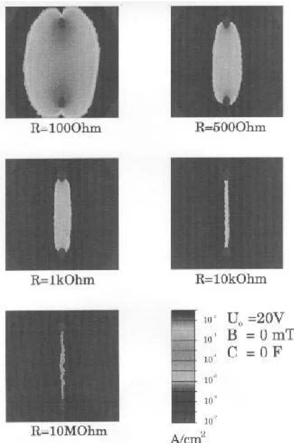
Fig. shows the fully developed stationary current laments for ve dierent values of a series load resis-tance R. At R= 100 the lament is very wide and
plum-shaped. With increasingRthe operating point on
the characteristic is shifted towards lower sample volt-age and current, and the width of the lament decreases and nally the lament becomes very unstable and thin (R= 10M). The change of the shape and the width
of the lament describes a transition from a pattern in-duced by the dipolar electric eld to a self-organized l-ament, in good agreement with experiments [16, 53, 5]. It has been found experimentally that an exter-nal magnetic eld applied perpendicular to the elec-tric eld can sensitively aect the spatio-temporal in-stabilities in the regime of impurity impact ionization [54, 55, 56]. The dynamic Hall eect has been pro-posed as a mechanism to induce chaotic temporal
os-cillations in the breakdown regime [57]. The transverse periodic or chaotic motion of a current lament un-der crossed electric and magnetic eld has been nu-merically analyzed for p-type Ge by one-dimensional simulations based on the semiclassical semiconductor-transport equations neglecting the longitudinal spatial dependence [38]. The spatial deformation of current laments in the presence of a transverse magnetic eld has been explained by an eectively one-dimensional drift-diusion model assuming a dipole-like electric eld between two point-contacts [41]. However, in order to fully understand the eects of a transverse magnetic eld on the lament properties, two-dimensional analy-ses including the spatial dependence on both the longi-tudinalx- and the transverse z-direction are
indispens-able [48].
The current densityj(B) in the presence of a
mag-netic eldB normal to the current ow is given by
j(B) =
j(0) +Bj(0)
1 +jBj 2
; (9)
wherej(0) is the current density forB= 0 as given by
Eq. (2).
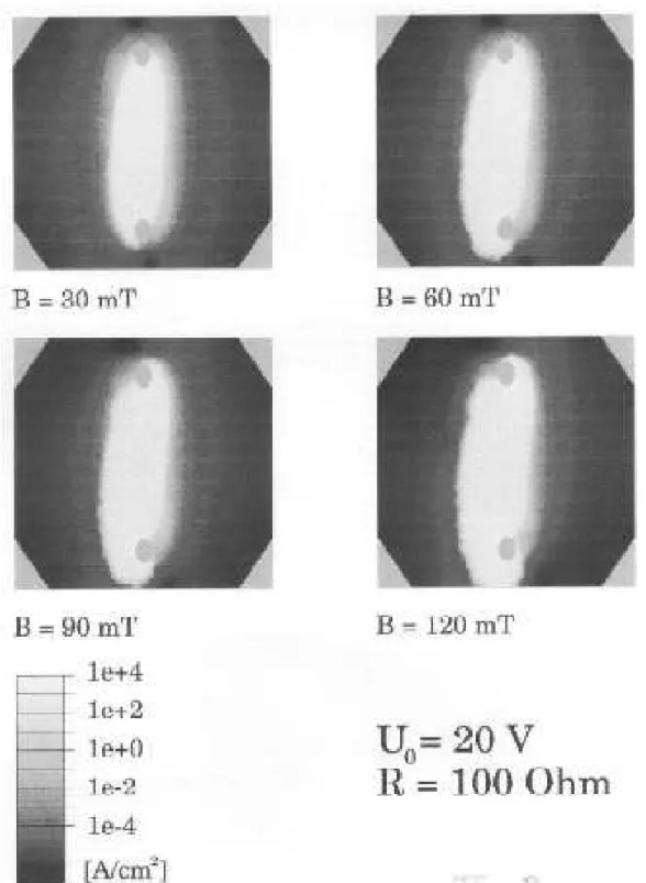
Upon application of a voltage ramp and a mag-netic eld of a few mT, rst a thin, straight lament is formed as in the case without magnetic eld. In the next stage, the straight lament is gradually widened and asymmetrically expanded in the direction of the Lorentz force [48]. The simulation shows that the elec-tric elds at the lament border pointing in the direc-tion of the Lorentz force are much stronger than at the opposite border. These asymmetric elds result from a superposition of the dipole eld due to the space charge already present in the lament walls atB= 0, and the
Hall eld. They are in good agreement with asymmet-ric ridge-like structures observed by scanning laser mi-croscopy under a transverse magnetic eld [11, 12, 41]. Also, the simulations and the experiments show that the width and curvature of the laments become larger with increasing magnetic-eld strength. Fig. shows the stationary current laments under the action of a magnetic eld for the same sample with two inner point contacts as in Figs. and . With increasingB the
la-ments become asymmetrically distorted by the Lorentz force, and at largeB and large currrent they assume an
Figure 1. Simulation of the formation of a current lament in n-GaAs. The temporal evolution of the current densityj(x;z)
after application of a bias voltage U0 = 20V via a load R = 100 is shown as a function of the spatial coordinates xand z for a rectangular sample with two inner point contacts for dierent times. Note that the injecting cathode is at the top
(calculated for T
L = 4.2 K with the parameters N
D= 7.0 10
15 cm,3, N
A= 2.0 10
15 cm,3, = 10
5 cm2/Vs,
r = 10.9,
Figure 2. Simulated current laments in a rectangular sample with two inner point contacts for an applied bias voltage
U0 = 50V and dierent load resistances R. The stationary current density jj(x;z)jis shown as a density plot. (calculated
Figure 3. Simulated current laments in a rectangular sample with two inner point contacts for an applied bias voltage
U
0= 20V,
Figure 4. Simulation of the formation of a current lament in a Corbino disk. The temporal evolution of the current density
jj(x;y)jis shown for a circular sample of diameter 2:1 mm and an inner contact diameter of 80m. a)t= 0:15 ns, b)t= 0:5 ns,
c)t= 0:7 ns, d) t= 1:7 ns e) t= 3:2 ns f)t= 9:9 ns. The bias voltage U 0 = 2
:4 V and the load resistanceR = 10 k
correspond to an operating point with an average eldE av= 4
:7 V=cm, i.e., between the holding eldE h= 4
:0 V=cm and
Figure 5. Simulated current-voltage characteristic of a circular sample with two concentric contacts of diameters 1 mm and 2.1 mm. The insets show the current density jj(x;y)jfor various operating points as indicated by arrows. The bias voltage U0 is swept from 2.0 to 36.5 V and the load resistance is R= 10 k (calculated with the same parameters as Fig. ).
III Current
laments
in
Corbino disks
Next, we present simulations of a sample with circular contact symmetry (Corbino disk). The sample is con-ned by an outer ring electrode of radius 1050m
(an-ode) and has a concentric inner point contact of 80m
diameter (cathode) in the center of the disk. Such ge-ometries oer the possibility to study pattern formation in samples without lateral boundaries, and are therefore of considerable interest. Various self-organized patterns of single and multiple current laments have been ob-served experimentally in such samples [59].
In our simulationa constant bias voltageU 0= 2
:4 V
is applied to the Corbino disk of thickness 3 m via a
load resistor R = 10 k. Initially the sample is in
the insulating state. Subsequently impact ionization multiplies the electron concentration at the injecting inner point contact and establishes a radially
symmet-ric front that moves towards the circular anode (Fig. (a)). At a certain radius the circular front breaks up into several streamers (b), each of which, upon reach-ing the anode, forms a rudimentary radial current la-ment (c). The symmetry of this pre-lala-mentary state, i.e. the number of rudimentary laments, depends on sample parameters as well as on the applied voltage. The pre-laments then start growing in current while retaining approximately their original width (d). This leads to a rising overall current I and thus, via the
ex-ternal load resistance, which acts as a global constraint due to Kirchho's law U
0 =
U +RI, to a reduction
in the sample voltage U. The pre-laments therefore
enter into a competition as a result of which only the lament which has rst reached the outer contact sur-vives (e). The other laments slowly decay into the low-conducting state and vanish (f).
is familiar from general nonlinear self-organizing pro-cesses under global constraints [60].
If the operating point is shifted to larger currents, more than one lament can survive. This is shown in Fig. where the bias voltageU
0is increased from 2.0 V
to 36.5 V. The insets show the stationary current den-sity distribution at dierent operating points for a sam-ple with two concentric contacts with diameters 1 mm and 2.1 mm. As the current increases, the current den-sity in the lament grows up to a threshold where a sec-ond lament is formed. This decreases the sample resis-tance, resulting in a switch-back of the sample voltage according to Kirchho's law. Thus a second branch of the current-voltage characteristic arises, corresponding to two laments. Similarly, successive branches with three, four, ve, etc. laments occur. Each jump in the current-voltage characteristic is associated with the generation of an additional lament. Hysteresis with respect to bias sweep-up and sweep-down is also found. Such behavior is in good agreement with experiments [59].
IV Conclusions
In this review we have presented concepts of spatio-temporal self-organization in semiconductors and illus-trated these by an exemplary model systems which has been in the center of recent theoretical and experimen-tal research. Investigations in diverse semiconductor materials and structures have led to an advanced under-standing of the complex dynamics of current laments in one and two spatial dimensions.
Inspite of the dierent microscopic nature of those systems some general principles of pattern formation and nonlinear spatio-temporal dynamics in semicon-ductors can be worked out. Considering the semi-conductor as an active medium which is governed by activator-inhibitor kinetics provides such a useful con-cept. Impact ionization of hot charge carriers plays the role of an activating autocatalytic process not only in the regime of low-temperature impurity breakdown, but is also important in multilayered semiconductor structures. The voltage across the device acts as an inhibitor, and global constraints resulting in a winner-takes-all dynamics are introduced by the external load. A modeling approach has been described which combines dierent levels of transport theory, and allows for a detailed understanding of both the microscopic scattering processes in the regime of impurity impact
ionization breakdown and the macroscopic dynamics of the laments for dierent two-dimensional (rectangular or circular) geometries.
ACKNOWLEDGEMENTS
I would like to thank C. Lehmann, F.-J. Niedernos-theide, V. Novak, W. Prettl, A. Reimann, P. Rodin, and G. Schwarz for stimulating discussions and collab-oration.
References
[1] E. Scholl,Nonequilibrium Phase Transitions in Semi-conductors(Springer, Berlin, 1987).
[2] M. P. Shaw, V. V. Mitin, E. Scholl and H. L. Gru-bin,The Physics of Instabilities in Solid State Electron Devices(Plenum Press, New York, 1992).
[3] B. S. Kerner and V. V. Osipov, Autosolitons(Kluwer Academic Publishers, Dordrecht, 1994).
[4] Nonlinear Dynamics and Pattern Formation in Semi-conductors and Devices, edited by F.-J. Niedernos-theide (Springer, Berlin, 1995).
[5] E. Scholl, F.-J. Niedernostheide, J. Parisi, W. Prettl and H. Purwins, in Evolution of structures in dissi-pative continuous systems, edited by F. H. Busse and S. C. Muller (Springer, Berlin, 1998).
[6] Theory of Transport Properties of Semiconductor Nanostructures, Vol. 4 ofElectronic Materials Series, edited by E. Scholl (Chapman and Hall, London, 1998). [7] A. Wacker and E. Scholl, J. Appl. Phys. 78, 7352
(1995).
[8] B. K. Ridley, Proc. Phys. Soc.82, 954 (1963).
[9] K. Mayer, J. Parisi and R. Huebener, Z. Phys. B71,
171 (1988).
[10] A. Wierschem, F.-J. Niedernostheide, A. Gorbatyuk and H.-G. Purwins, Scanning 17, 106 (1995).
[11] A. Brandl, M. Volcker and W. Prettl, Appl. Phys. Lett.
55, 238 (1989).
[12] J. Spangler, B. Finger, C. Wimmer, W. Eberle and W. Prettl, Semicond. Sci. Technol.9, 373 (1994).
[13] B. Kukuk, F. Reil, F.-J. Niedernostheide and H.-G. Purwins, inSelforganization in Activator-Inhibitor-Systems, edited by H. Engel, F.-J. Niedernostheide, H. G. Purwins and E. Scholl (Wissenschaft & Technik Verlag, Berlin, 1996), pp. 62{66.
[14] H. Baumann, R. Symanczyk, C. Radehaus, H. Purwins and D. Jager, Phys. Lett. A123, 421 (1987).
[15] F.-J. Niedernostheide, M. Arps, R. Dohmen, H. Wille-brand and H.-G. Purwins, phys. status solidi (b)172,
249 (1992).
[16] W. Eberle, J. Hirschinger, U. Margull, W. Prettl, V. Novak and H. Kostial, Appl. Phys. Lett. 68, 3329
191, edited by Y. Abe (1989).
[18] E. Scholl, in Handbook on Semiconductors, 2nd ed., edited by P. T. Landsberg (North Holland, Amster-dam, 1992), Vol. 1.
[19] A. Wacker and E. Scholl, Semicond. Sci. Technol. 9,
592 (1994).
[20] R. Stasch, R. Hey, M. Asche, A. Wacker and E. Scholl, J. Appl. Phys.80, 3376 (1996).
[21] A. Alekseev, S. Bose, P. Rodin and E. Scholl, Phys. Rev. E57, 2640 (1998).
[22] F.-J. Niedernostheide, B. S. Kerner and H.-G. Purwins, Phys. Rev. B46, 7559 (1992).
[23] M. Meixner, P. Rodin and E. Scholl, Phys. Rev. E58,
2796 (1998).
[24] M. Meixner, P. Rodin and E. Scholl, Phys. Rev. E58,
5586 (1998).
[25] Negative Dierential Resistance and Instabilities in two-dimensional Semiconductors, edited by N. Balkan, B. K. Ridley and A. J. Vickers (Plenum Press, New York, 1993).
[26] Z. S. Gribnikov, K. Hess and G. Kosinovsky, J. Appl. Phys.77, 1337 (1995).
[27] L. L. Bonilla, J. Galan, J. A. Cuesta, F. C. Martnez and J. M. Molera, Phys. Rev. B50, 8644 (1994).
[28] F. Prengel, A. Wacker and E. Scholl, Phys. Rev. B50,
1705 (1994), ibid52, 11518 (1995).
[29] H. T. Grahn, in Semiconductor Superlattices, Growth and Electronic Properties, edited by H. T. Grahn (World Scientic, Singapore, 1995), Chap. 4.
[30] A. Wacker, in Theory of transport properties of semi-conductor nanostructures, edited by E. Scholl (Chap-man and Hall, London, 1998), Chap. 10.
[31] F. Piazza, P. C. M. Christianen and J. C. Maan, Phys. Rev. B55, 15591 (1997).
[32] Quantum Transport in Ultrasmall Devices, edited by D. K. Ferry, L. Grubin, C. Jacoboni and A. P. Jauho (Plenum Press, New York, 1995).
[33] K. Aoki, T. Kobayashi and K. Yamamoto, J. Physique Colloque C7, 51 (1981).
[34] S. W. Teitsworth, R. M. Westervelt and E. E. Haller, Phys. Rev. Lett.51, 825 (1983).
[35] E. Scholl and D. Drasdo, Z. Phys. B81, 183 (1990).
[36] R. E. Kunz and E. Scholl, Z. Phys. B89, 289 (1992).
[37] G. Hupper, K. Pyragas and E. Scholl, Phys. Rev. B
47, 15515 (1993).
[38] G. Hupper, K. Pyragas and E. Scholl, Phys. Rev. B
48, 17633 (1993).
[39] R. E. Kunz and E. Scholl, Z. Phys. B99, 185 (1996).
52, 9023 (1995).
[42] T. Kuhn, G. Hupper, W. Quade, A. Rein, E. Scholl, L. Varani and L. Reggiani, Phys. Rev. B48, 1478 (1993).
[43] W. Quade, G. Hupper, E. Scholl and T. Kuhn, Phys. Rev. B49, 13408 (1994).
[44] B. Kehrer, W. Quade and E. Scholl, Phys. Rev. B51,
7725 (1995).
[45] H. Kostial, M. Asche, R. Hey, K. Ploog, B. Kehrer, W. Quade and E. Scholl, Semicond. Sci. Technol.10, 775
(1995).
[46] M. Gaa, R. E. Kunz and E. Scholl, in Proc. 9th Int. Conf. on Hot Carriers in Semiconductors, edited by K. Hess, J. P. Leburton and U. Ravaioli (Plenum, New York, 1996), pp. 347{351.
[47] M. Gaa, R. E. Kunz and E. Scholl, Phys. Rev. B 53,
15971 (1996).
[48] K. Kunihiro, M. Gaa and E. Scholl, Phys. Rev. B 55,
2207 (1997).
[49] G. Schwarz and E. Scholl, Acta Technica CSAV 42,
669 (1997).
[50] G. Schwarz, C. Lehmann and E. Scholl, in Proc. 24th International Conference on The Physics of Semicon-ductors (ICPS-24), Jerusalem, Israel, edited by D. Gershoni (World Scientic, Singapore, 1999).
[51] E. Scholl, Z. Phys. B46, 23 (1982).
[52] R. E. Kunz, E. Scholl, H. Gajewski and R. Nurnberg, Sol. State El.39, 1155 (1996).
[53] M. Gaa, R. E. Kunz, E. Scholl, W. Eberle, J. Hirschinger and W. Prettl, Semicond. Sci. Technol.11,
1646 (1996).
[54] A. Brandl, T. Geisel and W. Prettl, Europhys. Lett.3,
401 (1987).
[55] A. Brandl, W. Kroninger, W. Prettl and G. Obermair, Phys. Rev. Lett.64, 212 (1990).
[56] U. Rau, W. Clauss, A. Kittel, M. Lehr, M. Bayerbach, J. Parisi, J. Peinke and R. Huebener, Phys. Rev. B43,
2255 (1991).
[57] G. Hupper and E. Scholl, Phys. Rev. Lett. 66, 2372
(1991).
[58] J. Hirschinger, F. J. Niedernostheide, W. Prettl, V. Novak, M. Cukr, J. Oswald and H. Kostial, Acta Techn. CSAV42, 661 (1997).
[59] J. Hirschinger, W. Eberle, W. Prettl, F.-J. Niedernos-theide and H. Kostial, Phys. Lett. A236, 249 (1997).