www.adv-radio-sci.net/4/207/2006/ © Author(s) 2006. This work is licensed under a Creative Commons License.
Radio Science
Full dynamic resolution low lower DA-Converters
for flat panel displays
C. Saas, J. Franke, and J. A. Nossek
Institute for Circuit Theory and Signal Processing, Munich University of Technology, Germany
Abstract. It has been shown that stepwise charging can re-duce the power dissipated in the source drivers of a flat panel display. However the solution presented only provided a dy-namic resolution of 3 bits which is not sufficient for obtaining a full color resolution display. In this work a further develop-ment of the basic idea is presented. The stepwise charging is increased to 4 bits and supplemented by a current source to provide an output signal which represents an 8 bit value with sufficient accuracy. Within this work the application is an AM-OLED flat panel display, but the concept can easily be applied to other display technologies like TFT-LCD as well.
1 Introduction
1.1 Flat panel displays
Figure 1a depicts the common architecture of all flat panel matrix displays. Although the investigations in this work have been carried out to meet the requirements of an OLED display the basic concept is as well applicable to all other types of active matrix displays. Displays that feature a selec-tion transistor likeT1in Fig. 1b are considered to be active displays.
The proposals in this work apply to the column drivers in the display. They are as well called source drivers as the sources of the selection transistors in an active matrix display are connected to the output of this driver. This output has to provide an analog voltage value which corresponds to the in-tensity of a color sub-pixel. However, the row or gate drivers exhibit a digital output and are not covered in this work.
Please note that a flat panel display always needs calibra-tion due to the nonlinear behavior of the optical element. This nonlinearity has to be calibrated at least for each new product. In high accuracy applications like pre-press every
Correspondence to: C. Saas ([email protected])
transistor selection
source drivers
gat
e
dr
iv
er
s
CL
Vdd
a) b)
T1 T2
Fig. 1. (a) Architecture and (b) Pixel Schematic for an AM-OLED
Display.
single display has to be calibrated every month to maintain color matching. In the proposed architecture this calibration can be realized in hardware by means of the lookup table. This solution is saving valuable dynamic resolution in the control circuitry. Please note that calibration is carried out for the whole display. Therefore variations between adjacent column lines can not be corrected. These variations can be considered small enough to not influence the image quality.
In this work a total error of 10% in the final voltage level on the column line is considered acceptable. Please note, that this small error leads to a high quality display and is not met by most consumer products on the market today.
Examinations in this work are carried out for a 1000 times 1000 pixel display, a typical load capacitanceCL of 200 pF and an image refresh rate of 60 Hz. The voltage range for the pixel cell has been set to 0 V up to 5 V. The values chosen are exemplary for a wide range of display applications and are therefore well suited to evaluate the presented concepts.
Later calculations require the available time for charging a column line. The chosen image refresh rate corresponds to a time of 17 ms. This defines a time of 17µs for each row. Since all columns are charged simultaneously, this is also the available time for charging one column line.
Assuming 8 bits per pixel, neglecting the data overhead and calculating one million pixels to fit into one cycle of 60 Hz results in pixel data running at 480 MHz, respectively a cycle time of 2 ns for the pixel clock.
1.2 Stepwise Charging
Stepwise charging is a possible realization of adiabatic switching which exhibits the advantage of not needing an os-cillator. The concept of adiabatic switching has been well covered in literature (Athas et al., 2000; Ziesler et al., 2001). The necessary voltage ramps are approximated by small volt-age s.pdf, which reduces the dissipated energy to
Ediss,stepwise= 1
NEdiss (1)
whereNis the number of s.pdf.
Please note that this holds only true if the system is given enough time to settle. Therefore, stepwise charging is like all adiabatic switching techniques a tradeoff between power and speed and most suitable in applications with limited perfor-mance requirements (Saas and Nossek, 2002).
2 The stepwise driver
The basic concept of how to apply stepwise charging to the source drivers in a flat panel display has been presented at ISCAS 2004 (Saas et al., 2004). Although the presented so-lution had some limitations, it clearly demonstrated the pos-sibilities regarding power consumption.
The proposed architecture implements as many compo-nents as possible in the digital domain as to minimize the ef-fort in power and area for analog components. The presented DA converter is capable of driving the lines and therefore there is no need for analog line drivers. The digital registers consume significantly less energy than the analog counter-part. Although the new logicL′is slightly more complicated and one DAC is needed at each line, the power consumption is negligible with respect to the bias currents of the conven-tional line drivers.
Stepwise charging is realized by applying a digital control signal, which will switch the output to the next higher value for each time step until the desired voltage level is reached. To benefit from the possible power savings it is important to ensure that an intermediate voltage level is almost reached before the next clock edge. A significant part of the energy on the line can be reused by applying charge recovery. Large capacitors are used to temporarily deliver energy and to re-cover the charge when driving analog output voltages.
There is one large source capacitorCsper reference volt-age. It is charged by reference voltage sources to the ap-propriate voltage level during the reset period. Afterwards the whole DAC is powered from the capacitors. As there is only one reference voltage generator per display, the source capacitors could be realized as external elements.
The output is discharged stepwise by connecting the load to the appropriate reference voltages. Thus every clock cycle the output voltage is decreased byVfull/N. When the output is connected to the next lower reference voltage level some of the charge is transferred back toCs and the correspond-ing reference voltage acrossCsis nearly restoring the initial value. Of course, there can be no energy transferred to the highest voltage level. The amount of energy taken from this reference voltage is prorated on the charging and discharg-ing of the sdischarg-ingle s.pdf. In the followdischarg-ing reset the losses are compensated by connectingCs to the appropriate reference voltage. It can easily be calculated that in theory all but the highest source capacitorsCs max recover charge up to their original voltage value. The energy which has been dissipated and thus has to be replaced inCs maxis given by
Es max= Vfull
N ·Vmax·CL (2)
where Vmax is the voltage the line was charged up to and Cs maxthe corresponding source capacitor.
Although this driver has been presented for a 3 bit resolu-tion, it can easily be scaled to 4 bit.
3 Increasing bit depth
Up to date color displays for mobile applications require at least a 6 bit resolution per color to be competitive. To obtain a full dynamic color resolution, a bit depth of 8 bit is required. Higher bit depths in a display are usually used for calibration reasons and are obsolete when other means of color calibra-tion are provided.
The scaling of the driver proposed in Sect. 2 is not a suit-able approach to obtain a higher dynamic resolution as this would increase the number of supply capacitances and low impedance voltage sources thus leading to an unacceptable overhead. In this work a hybrid solution is proposed. Step-wise charging is used to generate an approximated output level corresponding to the 4 most significant bits (MSB) and a second stage is evaluating the 4 least significant bits (LSB) to obtain an accurate voltage level. Due to a number of sys-tematic offset errors some means of calibration has to be provided.
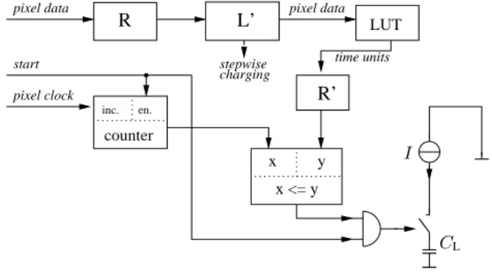
3.1 Adding a defined charge
y x
x <= y
time units
LUT
R L’ pixel data
charging stepwise start
pixel clock pixel data
R’
en. inc.
counter
CL
I
Fig. 2. Architecture of the full dynamic resolution driver.
can be set by adding a certain amount of charge. 1V =Q
C (3)
Assuming a constant charging current, the voltage difference is determined by the on time of the current. Even in the case of a not perfectly constant current the time values to obtain a correct pixel value can be easily obtained by calibration.
The final voltage levels are not taken from a reference volt-age but are locally evaluated in the driver. The proposed so-lution exhibits the advantage of a reduced number of refer-ence voltage lines from the referrefer-ence voltage generator to the source drivers. This goes very well along with the indus-try standard proposed by National Semiconductor which also reduces the number ofVreflines by generating intermediate levels locally in the driver (McCartney, 2004).
3.2 The current sources
Current sources are typically realized by a current mirror. In the present application additional switching requirements ex-ist which are not covered by the standard CMOS current mir-ror; a modified current mirror is introduced.
The reference currents are generated by a standard bias generator. This current has to be mirrored several times ac-cording to the number of source drivers. As the pixel-value is in general different for each column, each of the current mir-rors has to be independently switchable. This is not possi-ble with a standard CMOS mirror, as the switching transistor would introduce a significant mirror error during operation. The proposed circuit is shown in Fig. 3.
Analytical proof of the proper function of the proposed cir-cuit is only carried out for equally sized transistorsT1,T2,T3 andT4. Nevertheless, the current mirror also works for other transistor sizes which may be desirable to avoid devices in non-saturation region. Please note that channel length mod-ulation is neglected. ForT2 andT3 in saturation, it is ob-vious, thatIds2equalsIds3. However, it also holds true for (W/L)2=(W/L)1.
CL Vdd
T1
T2 T3
T4
I
Iref
Fig. 3. Schematic of a switchable current source.
The conditions for a PMOS transistor to be in saturation are
Vgs< Vth,P (4)
Vds≤Vgs−Vth,P (5)
ForT1Eq. (4) is satisfied, otherwise it would be in cut-off mode, which is impossible as long asIsd1=Iref≥0. Equa-tion 5 is satisfied, too, sinceVds1=Vgs1andVth,P<0. Obvi-ously,T2is in non-saturation, because its current equalsIsd1, butVgs26=Vgs1and differentVgsfor identical transistors that are both saturated lead to different currents. Thus,T1 is in saturation,T2in non-saturation mode. Note that all voltages ofT1andT2are independent of the supply voltageVdd. For T4, Eq. 5 is satisfied if
Vds4≤Vgs4−Vth,P. (6)
or
Vds4+Vds3≤Vgs3−Vth,P. (7) The sum ofVds4andVds3depends on the voltage on the load capacitance and onVdd. Thus, we must apply an adequate supply voltage. T4 is in saturation mode and T3 in non-saturation mode as explained above. The drain currents of T3andT4have to be equal:
Ids3=Ids4. (8)
Plugging in the transistor equations gives Kp(Vgs3−Vth,P−
Vds3 2 )Vds3=
Kp
2 (Vgs4−Vth,P)
2 (9)
Please note that the proposed circuit has no improvement over the standard mirror with respect to the mirror error, but it has additional switching capabilities.
To fulfill timing requirements in the display, a minimum charging current has to be applied. In the worst case the load capacitance has to be charged a full MSB-step within one cycle. Charging time for a 17µs cycle may last up to 4µs.
Imin= 1
16VmaxCL
tmax ≈16µA (10)
On the other hand, there is also an upper bound due to ac-curacy requirements. As the timet is derived from a clock signal, there are quantization errors in the charging timet. Imax= .pdf ilonmax·CL
tmin
≈78µA (11)
where.pdf ilonmaxis the maximum acceptable error. 3.3 Preset values for the lookup table
Due to variations in the current with respect to the output voltage the lookup table has to hold a number of charging time units for each of 256 possible output values. Neverthe-less, this small amount of memory is negligible in compari-son to the analog parts of the driver. The values in the lookup table can be easily obtained by color calibration of the dis-play and set by a software tool.
However, calculating this values systematically delivers a preset for the table. For this purpose, a reasonable model of the current is required. The current versus load voltage is not linear. However, since only small changes of the output value due to the LSBs are of interestI can be approximated with good accuracy by
I =I0−α1V , (12)
whereI0is the current at LSB 0000 andαthe negative slope. αcan be easily derived from the current values of two adja-cent MSB values.
As we know that CL1V =
Z t
0
I dt, (13)
we derive
⇒1V + α
CL Z t
0
1V dt= I0t
CL (14)
and d dt1V +
α CL
1V = I0 CL
. (15)
The solution to this differential equation is given by 1V =I0
α(1−e −Cα
Lt). (16)
Therefore, the charging time is given by t= −CL
α ln(1−α 1V
I0
). (17)
Equation 17 gives a good approximation for the charging time.
In addition, the delay between the switching signal and the output current has to be taken into account. On the one hand, there is a significant delay between the transition of the control signal and the current reaching its nominal value. On the other hand the current is not cut off immediately af-ter the control signal returns to the off state. These delays have to be considered and the time values have to be adjusted accordingly.
3.4 Fine adjustment and Gamma correction
Today’s liquid crystal flat panel displays need extensive gamma correction due to nonlinearities in the voltage - trans-mission curve. The properties of the crystal vary over time, so the display needs to be calibrated if accurate color repro-duction is an issue. Although the nonlinearities for the opti-cal emission with respect to the current are much weaker in an OLED display, there is still the need for calibration. In the proposed circuit, gamma correction and calibration can be carried out rather easy by adjusting the values in the lookup-table. This can be done during runtime by a software tool. 3.5 Energy performance of the LSB part
As the energy performance of the stepwise MSB part is well understood (Saas et al., 2004), this section will only cover the additional dissipation due to the LSB part. The gener-ation of the reference currents and the reference part of the mirror supply a significant number of source drivers and can be neglected.
The energy taken from the supply by a single source driver during charging is given by
Ecurrent source=Vdd·Iref·t =CL·Vdd·1V (18) Please note that the supply voltage Vdd is higher than the maximum output voltage. Table I shows the calculated val-ues for some LSB valval-ues. A significant part of the en-ergy delivered by the LSB part is stored onto the load capacitanceCL.
Eadditional=CL·1V ·VMSB− 1
2CL·1V
2 (19)
This energy can be recovered during stepwise discharging and reduces energy losses in the MSB part.
3.6 Voltage follower based solutions
Table 1. Calculated energy for selected LSBs.
LSB Desired voltage Ideal charging Delivered code level /mV time /ns Energy /pJ 0000 0000.00 0.0 0.000 0001 0019.53 195.3 31.25 0101 0097.66 976.6 156.25 1011 0214.84 2148.4 343.74 1111 0292.97 2929.7 468.75
Table 2. Simulation result for the MSB part.
conventionalCV2 N1CV2 simulation
3 bit driver 294µW 42.0µW 46.3µW
4 bit driver 294µW 19.6µW 22.4µW
4 Simulation results
Simulations have been carried out using a 180 nm CMOS process. In addition some high voltage devices where used due to the required output voltage range. These technologies are not used in real display production, but they are suffi-ciently similar to allow a good estimation of the possibilities of this new concept.
4.1 MSB part
The power consumption of the improved stepwise driver scales very well with the increased number of s.pdf. The simulation results as well as theoretical estimations are listed in Table 2. As expected the energy dissipation is even smaller than that of the three bit driver due to the smaller step-size. The gain of both with respect to the conventional solution is obvious.
Further elaborations on the simulation results of the step-wise driver can be found in Saas et al. (2004).
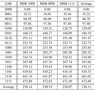
4.2 LSB part
The simulations results of the LSB part are shown in Table 3. Results are listed for all LSB values at some representative MSB values. Although results are slightly different for dif-ferent MSB values, it can be seen, that simulations corre-spond very well with the estimations made in Sect. 3.5. The average values listed in the table have been calculated assum-ing an equally distribution of pixel values. Additional simu-lations have been carried out to evaluate power consumption due to leakage currents. The total power consumption due to static parasitic effects was in the worst case 0.0034 pJ over a whole cycle. This small amount is negligible with respect to the dynamic power consumption.
Table 3. Simulated delivered energy for charging LSBs in pJ.
LSB MSB 1000 MSB 0000 MSB 1111 Average
0000 0.00 0.00 0.00 0.00 0001 35.31 34.91 35.44 35.22 0010 66.58 66.68 66.83 66.70 0011 97.84 97.56 97.40 97.60 0100 129.09 129.31 128.75 129.05 0101 160.32 160.17 160.09 160.19 0110 191.11 191.91 191.40 191.47 0111 222.75 222.74 222.71 222.73 1000 253.95 253.56 253.99 253.83 1001 285.14 285.27 285.26 285.22 1010 316.31 316.96 316.51 316.60 1011 347.48 347.76 347.74 347.66 1100 379.12 379.43 378.96 379.17 1101 410.61 410.22 410.16 410.33 1110 441.74 441.87 441.34 441.65 1111 472.86 472.63 472.49 472.66
Average 238.14 238.19 238.07 238.13
As explained in Saas et al. (2004) no conventional driver has been designed and simulated as a reference. It has been shown the the proposed architecture minimizes energy con-sumption to about 10% of a theoretical lower bound. The simulation results for the improved driver with a dynamic resolution of 8 bit show the power consumption is in the same order of magnitude. The average power consumption of 238.13 pJ translates into 14µW for the clock cycle of 17µs. Even if the additional charge-recovery during dis-charging is not taken into account, the new driver still con-sumes significantly less than the conventional solution.
5 Conclusions
The performance of the proposed architecture proves that stepwise charging is well suited to reduce power dissipation in the source driver in a full color resolution display. The energy consumption can be significantly reduced while pre-serving accuracy for the voltage levels and meeting timing constraints for typical display resolutions.
References
McCartney, R.: A third generation timing Controler and column driver architecture using point-to-point differential signaling, in: Proceedings of SID Symposium, Seattle, 2004.
Saas, C. and Francke, J.: Increasing Bit Depth in Low Power DA-Converters for Display Applications, Tech. Rep. TUM-LNS-TR-04-7, Munich University of Technology, 2004.
Saas, C. and Nossek, J.: Resonant Multistage Charging of Domi-nant Capacitances, in: Proceedings of PATMOS, Sevilla, 2002.
Saas, C., Wr´oblewski, A., and J.A.Nossek: Low-Power DA-Converters for Display Applications using Stepwise Charging and Charge Recovery, in: Proceedings of ISCAS, Vancouver, 2004.