336 Brazilian Journal of Physics, vol. 36, no. 2A, June, 2006
Magnetotransport in Al
x
Ga
x−
1
As Quantum Wells with Different Potential Shapes
N. C. Mamani, C. A. Duarte, G. M. Gusev, A. A. Quivy, and T. E. Lamas
Instituto de F´ısica da Universidade de S˜ao Paulo, CP 66318, CEP 05315-970, S˜ao Paulo, SP, Brazil
Received on 4 April, 2005
We compare the transport properties for triangular, parabolic and cubic quantum wells. We calculate the transport mobility for electrons belonging to the different subbands. We obtain the energy spacing between first and second subbands from the electron sheet density and compare results for different potential profiles. We find that experimental results are in quantitative agreements with our calculations.
Keywords: AlxGax−1As; Transport properties; Quantum wells
I. INTRODUCTION
Recent progress in Molecular Beam Epitaxy (MBE) growth methods has made possible the creation of electronic systems with unusual and interesting properties. Well-known exam-ples are double quantum wells, quantum dot array in different configurations and combination of layers and quantum dots [1–3]. MBE growth also can be used to grow quantum wells, when electrons are confined in potential with various profiles U(z) =U0|z/W|n, where W is the well-width parameter, U0
is the potential height and n is number, which, is equal to 1 for triangular well and n=2 for parabolic well. Energy levels for these different potential wells have a different dependence on the quantum numbers. For example energy levels for the square well of infinite height are proportional to the square of the quantum number. For the parabolic well of infinite height the energy levels are evenly spaced. The energy lev-els for the potential U(z) =U0|z/W|2/3exhibit a square-root
dependence on the quantum number [4]. It is expected, that for low electron density in the well the ”bare” potential is not screened and energy spectrum is not strongly modified. Since the many transport properties of electrons depend on the shape of the wave function and quantum well profile, it will be useful to identify the most suitable quantum well structure for new electronic devices development. In present paper we grew and studied AlxGax−1As quantum wells with potential shapes U(z) =U0|z/W|n , where n=1,2 and 3. For magnetic field
oriented perpendicular to the sample a series of equidistant Landau levels are developed for the two-dimensional electron gas (2DEG), and magnetoresistance manifests Shubnikov -de Haas (SdH) oscillations. From analysis of the SdH oscilla-tions we may deduce electron density for all electric subbands. In present paper we grew triangular, parabolic and cubic Ga1−cAlcAs quantum wells and compared its transport prop-erties.
II. EXPERIMENTAL RESULTS AND DISCUSSIONS
The samples were made from Ga1−cAlcAs quantum wells grown by molecular -beam epitaxy. It included a 2000 ˚A -wide Ga1−cAlcAs wells with Al content varying between 0 and 0.21, bounded by undoped Ga1−cAlcAs spacer layers with δ−Si doping on two sides [6]. The mobility of the electron gas in our samples was∼(100−350)×103cm2/V s and
den-sity - ns= (2−4)×1011cm−2, therefore our quantum wells were partially full with 1-4 subbands occupied. Four -terminal resistance Rxx and Hall Rxy measurements were made down to 1.5 K in a magnetic field up to 12 T. The characteristic bulk density for parabolic quantum well is given by equation
n+=Ω 2 0m∗ε
4πe2 . The effective thickness of the electronic slab can be obtained from equation We f f =ns/n+. For partially filled quantum well Weis smaller than the geometrical width of the well W . We varied the electron sheet density by illumination with a red light-emitting diode.
-1000 -500 0 500 1000 0
50 100
0,0 2,0x10¹⁶ -1000 -500 0 500 1000 0
50 100
0 1x10¹⁷
(b)
z (Å)
E
n
e
rg
y
(
m
e
V
) (a) De
n
s
ity
(
c
m
-3
)
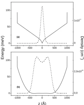
FIG. 1. Total potential (solid line) and electron density (dashes) as a function of position in the well for triangular (a) and parabolic quan-tum wells (b) before illuminations (ns=2.4×1011cm−2).
Table 1. Comparison of the triangular and parabolic quantum wells for ns=2.4×1011cm−2. N is the number of occupied
subbands.
Sample N EF−E1 EF−E2 EF−E3 ∆
meV meV meV A˚
parabolic 3 4.2 2.85 0.56 819
N. C. Mamani et al. 337
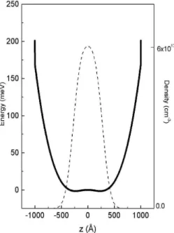
We performed full self-consistent calculations of the total potential, envelope wave functions, the eigenvalues energies and electron density in quantum wells with different shapes following a procedure similar to those used for parabolic quantum wells [5, 6]. Figs.1 and 2 show the electron density profile and total potential for triangular, parabolic and cubic quantum wells. We may see that the electronic slab width in parabolic quantum well is wider than in triangular well for the same carrier density. For cubic profile the quantum well is al-most full for low electron density, therefore we are not able to do such comparison. The density profile depends on the number of substantially occupied subbands: when only one subband is occupied, the density profile is sharply peaked, as we see for triangular well. The table 1 summarize the results of the calculations of the Fermi level for different subbands in parabolic and triangular wells.
FIG. 2. Total potential (solid line) and electron density (dashes) as a function of position in the well for U(z) =U0|z/W|3quantum well,
ns=0.6×1011cm−2.
We also calculate single particle relaxation time and trans-port relaxation time due to the background impurity doping. It is worth to note that the single particle relaxation time, or quantum time describes the decay time of one-particle excitations and give rise to the renormalization of the density of states in contrast to the transport relaxation time, which describes the mobility of an electron gas. The quantum times are obtained by numerical integration the squared matrix elements over the allowed scattering vector using self con-sistent calculated wave function. Screening of the impurity scattering potential in the presence of the 2D electron gas is included within the Thomas-Fermi approximation. A detailed calculation of the quantum and transport times should include the different scattering mechanism such as homogeneous background scattering, interface roughness scattering and
alloy disorder scattering. The scattering time contains many parameters, such as concentration of the background impurities, which can be enhanced in parabolic well due to the greater reactivity of Al with oxygen, and roughness of the interfaces.
0 1 2 3 4 5
105 106
Calculated parabolic triangular cubic
Experimental parabolic triangular
M
o
b
ili
ty
(
c
m
2 (/
V
.s
)
ns (x1011 cm-2)
FIG. 3. The total mobility was calculated as a function electron density for parabolic, triangular and cubic wells. Solid circles-experimental results for triangular well, crossed circle-circles-experimental mobility for parabolic well.
We do not attempt to calculate all scattering mechanisms accurately, because we are only interested its density profile behaviour. Since the wavefunction in our structures are lo-cated mostly in the center of the well we ignore the remote impurity scattering mechanism and suppose that the back-ground impurities should be a major scattering mechanism in this case. It is worth to note that in the multi-subband systems the intersubband scattering starts to play very important role. For a system with N subbands occupied the quantum time is given by
1/τi q=
N
∑
j=1
Pi j0. (1)
338 Brazilian Journal of Physics, vol. 36, no. 2A, June, 2006
0 2 4 6 8 10
0 2 4
R xx
(a
rb
.
u
n
it
s)
Perpendicular field (T) parabolic triangular
FIG. 4. Magnetoresistence as a function of the perpendicular mag-netic field for parabolic (thin line) and triangular ( thick line) quan-tum wells, T=1.5 K.
The transport life timeτi
trhas a more complicated form and can be obtained from the Boltzman equation [7]:
kiτtri = N
∑
j=1
(Ki j)−1kj. (2)
where the scattering matrix Ki jis defined as:
Ki j= N
∑
j=1
Pi j0δi j−Pi j1. (3)
The coefficient Pi j0 is the transition rate integrated over the allowed scattering vectors, and Pi j1 is the first component of the Fourier transform of this transition rate. The intersubband scattering terms appear both in the diagonal and off-diagonal matrix elements. However, our system is symmetrical and the intersubband scattering between subbands of different parities vanishes. We invert the matrix Ki jnumerically, and obtain the transport life time for electrons in each subband. The effective average mobility is given by:
µ=
N
∑
j=1 niµitr
ns
. (4)
where µitr= (e/m)τi
tr . We fit the calculated mobility to the measured one for parabolic well and obtain background im-purity concentration Nimp=1.2×1014cm−2.
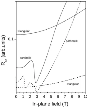
0 1 2 3 4 5 6 7 8 9 10
0,1 parabolic
triangular triangular
R
xx
(
a
rb
.u
n
it
s)
In-plane field (T)
parabolic
FIG. 5. Magnetoresistance as a function of the in-plane magnetic field for parabolic and triangular quantum wells, before illuminations ( thick line) and after some short illumination by red diode ( dashes), T=1.5 K.
N. C. Mamani et al. 339
III. CONCLUSION
We report the comparison of the transport properties for tri-angular, parabolic and cubic quantum wells. We calculate the transport mobility for electrons belonging to the different sub-bands and find that triangular well has higher mobility. In the presence of an electric field the minimum of the confining po-tential may be displaced with the center of the well, whereas the implicitly of the envelope of the wave function is con-served. This particular property of the partially filled
triangu-lar well makes it suitable for the practical realization of the electronic devices based on the manipulation of the g-factor for spintronic application[8].
Acknowledgments
Support of this work by FAPESP, CNPq (Brazilian agen-cies) is acknowledged.
[1] J. P. Eisenstein, L. N. Pfiefer, and K. W. West, Phys. Rev. Lett.
69, 3804 (1992).
[2] A. P. Alivisatos, Science, 271, 933 (1999).
[3] A. S. G. Thornton, T. Ihn, P. C. Main, L. Eaves, K. A. Benedict, and M. Henini, Physica B 249-251, 689 (1998).
[4] S. K. Sputz, A. C. Gossard, Phys. Rev. B 38, 3553 (1988). [5] A. J. Rimberg, R. M. Westervelt, Phys. Rev. B 40, 3970 (1989).
[6] C. S. Sergio, G. M. Gusev, J. R. Leite, E. B. Olshanetskii, N. T. Moshegov, A. K. Bakarov, and A. I. Toropov, D. K. Mau-de, O. Estibals, and J. C. Portal, Phys. Rev. B 64, 115314 (2001). [7] E. Zaremba, Phys. Rev. B 45, 14143 (1992).