Guilherme Ramos Castelo
Bachelor in Micro and Nanotechnologies Engineering
Ambient-processed Low-cost Perovskite-based
Photovoltaics
Dissertation to obtain the degree of Master of Science in
Micro and Nanotechnologies Engineering
Adviser: Dr. Manuel J. Mendes, Assistant Professor, Faculty of Sciences and Technology – New University of Lisbon
Co-Adviser: Dr. Ugur Deneb Menda, Pos-Doc Fellow, Faculty of Sciences and Technology – New University of Lisbon
Examination Committee:
Chairperson: Dr. Rodrigo Ferrão de Paiva Martins Raporteur: Dr. João Manuel Gregório Mascarenhas
Member: Dr. Manuel João de Moura Dias Mendes
III
Ambient-processed Low-cost Perovskite-based Photovoltaics
Copyright © Guilherme Ramos Castelo, Faculdade de Ciências e Tecnologia, Universidade NOVA de Lisboa, 2019.
A Faculdade de Ciências e Tecnologia e a Universidade NOVA de Lisboa têm o direito, perpétuo e sem limites geográficos, de arquivar e publicar esta dissertação através de exemplares impressos reproduzidos em papel ou de forma digital, ou por qualquer outro meio conhecido ou que venha a ser inventado, e de a divulgar através de repositórios científicos e de admitir a sua cópia e distribuição com objetivos educacionais ou de investigação, não comerciais, desde que seja dado crédito ao autor e editor.
V
vii
Acknowledgements
Primeiramente quero agradecer ao Prof. Dr. Rodrigo Martins e à Prof. Dra. Elvira Fortunato por me garantirem todas as condições de trabalho para realizar a minha tese, graças às excelentes instalações e equipamento ao dispor de todos os estudantes de materiais e nanotecnologias, no CENIMAT e no CEMOP. Em especial atenção agradeço aos meus orientadores Prof. Manuel Mendes e Dra. Deneb Menda por me terem dado a oportunidade de investigar na área da energia solar, a qual me cativa bastante e que irá ter ainda mais importância na nossa sociedade nos próximos tempos. Quero também agradecer a toda a equipa do CENIMAT e do CEMOP pela ajuda prestada sempre que necessitei.
I want to give a special thanks to my co-adviser, Dra. Deneb Menda, for everything that has done for me during these months working on the laboratory, all the work and life advices, all the time explaining and helping me in the laboratory, all the e-beam depositions, for never giving up, for always trying to motivate me when the work was not going well and for always being a positive person.
Não posso deixar de agradecer aos meus camaradas do CENIMAT que me acompanharam nesta caminhada difícil, bem como aos amigos que fiz ao longo destes 5 anos magníficos e que sempre me apoiaram nas alturas mais difíceis, com os quais vivi momentos e histórias incríveis e memoráveis e com os quais espero vir a recordá-las ao longo da nossa vida, sempre com a mesma amizade, alegria e cumplicidade, tais como o Guilherme Ferreira, Luís Bettencourt , Renato Nora, Joan Concha, João Vieira, Mafalda Pina, Mariana Moniz, Inês Tavares, Joana Rodrigues, entre outros.
Por fim, não posso deixar de agradecer à minha família, principalmente à minha mãe, pai, avós e tia que sempre me motivaram e apoiaram nos momentos mais complicados da minha vida académica em que por vezes me sentia desanimado e sem esperanças, e também por sempre tentarem fazer de mim uma pessoa melhor através dos seus ensinamentos e carinho que sempre me deram ao longo de toda a vida.
ix
Abstract
Perovskite solar cells (PSC) are one of the most promising photovoltaic (PV) technologies due to their quick and simple production, as well as their exceptional optoelectronic properties. However, their high price compared to the commercialized Si-based solar cells and their low scalability are some drawbacks that must be overcome.
In this thesis, these drawbacks were surpassed by substituting the costly materials by low-cost alternatives. Instead of Spiro-OMeTAD [1] as the hole transport material (HTM), a much cheaper material, CuSCN was used [2]. Furthermore, all the fabrication processes were performed in air under ambient conditions, avoiding the high cost and scalability problems associated with the use of a glove box. Considering this philosophy of low-cost development of the PSCs, the active layer was composed by MAI and PbI2 as the precursors, which were dissolved in γ-Butyrolactone (GBL), while maintaining the TiO2 as the electron transport material (ETM). Incisive analysis of the individual layers of the solar cells were performed by many characterization tools such as spectrophotometry, XRD and SEM-EDS.
As a result of several optimizations, a solar cell with VOC, JSC, FF and PCE values of 0.86 V, 15.29 mA/cm2, 0.64 and 8.48%, respectively was fabricated surpassing the previous efficiency record of 6.35% obtained in previous works [3].
xi
Resumo
Células solares de perovskita (PSC) são uma das mais promissoras tecnologias fotovoltaicas (PV) devido à sua produção rápida e simples, bem como às suas excecionais propriedades optoeletrônicas. No entanto, o seu elevado preço, comparativamente ao das células solares de silício comercializadas, e a sua baixa escalabilidade, são inconvenientes que devem ser ultrapassados.
Nesta tese, estes inconvenientes são ultrapassados através da substituição dos materiais mais caros por alternativas de baixo custo. Em vez de ser Spiro-Ometad [1] o material transportador de buracos (HTM), é utilizado um material muito mais barato, o CuSCN [2]. Para além disso, todos os processos de fabricação foram realizados em condições ambientais normais, evitando assim os custos e problemas de escalabilidade associados à utilização de uma “glove box”. Considerando esta filosofia de desenvolvimento de células de perovskita com baixo custo, a camada ativa é composta por MAI e PbI2 como percursores, que foram dissolvidos em γ-Butirolactona (GBL), mantendo-se o TiO2 como o material transportador de eletrões (ETL). Uma análise incisiva de todas as camadas foi efetuada, usando diversas ferramentas de caracterização, como espectrofotometria, XRD ou SEM-EDS.
Como resultado de várias otimizações, foi obtida uma célula solar com PCE de 8.48%, com VOC de 0.86 V, JSC de 15.29 mA/cm2 e FF de 0.64, superando assim o recorde de eficiência de 6,35% obtido nos trabalhos anteriores [3].
Palavras-chave: Células Solares de Perovskita, Dispositivos Fotovoltaicos de Baixo Custo, CuSCN, MAPbI3, Spin-Coating
xiii
Contents
List of Figures ... xv
List of Tables ...xix
Symbols ...xxi
Acronyms ... xxiii
Motivation and Objectives ... xxv
1. Introduction ...1
History of Solar Cells ...1
1.2.1 Perovskite Properties ...2
1.2.2 Architecture and Configuration ...3
1.2.3 Device Preparation and Fabrication ...4
2. Methods and Materials ...7
Device Fabrication ...7
2.1.1 Substrate Preparation and ETL deposition...7
2.1.2 Perovskite Solution Preparation and Deposition ...8
2.1.3 HTL and Top Electrode Depositions ...8
Characterization...8
2.2.1 SEM-EDS ...8
2.2.2 XRD ...8
2.2.3 UV-Vis-NIR Spectroscopy ...8
2.2.4 Opto-electrical Characterization. ...8
3. Results and Discussion ...9
ETL Layer Composition ...9
Perovskite Layer ... 11
3.2.1 Effect of MAPbI3 solution concentration ... 11
3.2.2 Effect of the toluene (anti-solvent) volume ... 14
3.2.3 Effect of the Annealing Temperature of the Perovskite Layer ... 17
3.2.4 Effect of the Annealing Time of the Perovskite Layer ... 19
HTL CuSCN Parameters ... 21
3.3.1 Effect of CuSCN Solution Concentration ... 21
3.3.2 Effect of CuSCN Volume Deposited ... 23
xiv
4. Conclusions and Future Perspectives ... 31
Future Perspectives ... 32
Bibliography ... 33
Appendices ... 41
A. Solar Cell Parameters ... 41
B. Materials... 42 C. Solutions Preparation ... 43 1. ETL ... 43 2. Perovskite Solutions ... 43 D. Optical Characterization ... 44 E. Opto-electronic Characterization ... 45
xv
List of Figures
Figure 1 - Plot describing the best efficiencies obtained by all types of solar cells. (This plot is courtesy of the National Renewable Energy Laboratory, Golden, CO). ...1 Figure 2 - Representation of the energy conversion process of a solar cell [12]. ...2 Figure 3 - Crystal structure of perovskites with the generic ABX3 configuration [25]. ...3 Figure 4 - Schematics of the most used configurations of a perovskite solar cell (PSC): a) n-i-p mesoscopic, b) n-i-p planar, c) p-i-n planar, d) p-i-n mesoscopic [33]. ...4 Figure 5 - Diagram of the energy level alignment of PSC layers used in this work (Based on [41]). ...5 Figure 6 - Perovskite solar cell (PSC) layers deposition steps and corresponding annealing conditions. This work employed the conventional n-i-p superstrate configuration (Figure 4a). ...7 Figure 7 - a) Absorbance spectrum of only the ETL deposited over FTO, with only compact TiO2 layer (blue) and also with Mesoporous TiO2 over it (red), as well as the representation of the ETL architecture; b) Transmittance and Reflectance spectra of the same ETL. ... 10 Figure 8 - a) J-V and b) P-V measurements of four solar cells with different ETL, which are composed of: 1x c.TiO2 (black), 2x c.TiO2 (cyan), c.TiO2 + mp.TiO2 (red) and c.TiO2 + mp.TiO2 + Li-TFSI (blue). ... 10 Figure 9 - a) Absorbance, b) Transmittance and reflectance spectra of three devices, which structure is illustrated on a), that are composed of perovskite layers that have different solution concentrations: 0.8 M (blue), 1 M (red) and 1.2 M (black). ... 12 Figure 10 - XRD results of the samples (all layers deposited except gold) fabricated with different perovskite concentrations: 0.8 M (blue), 1 M (red) and 1.2 M (black). Tetragonal perovskite crystal structure peaks marked with full circle; PbI2 peaks marked with open circle; FTO peaks marked with asterisk; CuSCN peaks marked with cardinal... 13 Figure 11 - a) J-V and b) P-V curves of three solar cells with different perovskite layer concentrations: 0.8 M (blue), 1M (red) and 1.2 M (black). ... 14 Figure 12 - a) Absorbance, b) Transmittance and reflectance spectra of three samples, whose structures are illustrated in the inset in a), that are composed of perovskite layers that were washed by toluene volumes of: 80 μL (red), 130 μL (black) and 200 μL (blue)... 15 Figure 13 - Top-view SEM images of cells with perovskite layers washed by different toluene volumes: a) 80 μL, b) 130 μL, c) 200 μL. The samples are composed of all the layers with the exception of the gold contacts. ... 15 Figure 14 - a) J-V and b) P-V curves of three solar cells with different volumes of toluene washing deposited: 80 μL (red), 130 μL (black) and 200 μL (blue). ... 16
xvi
structures are illustrated on a), that are composed of perovskite layers annealed at a temperature of: 65ºC (black), 110ºC (red) and 125ºC (blue). ... 17 Figure 16 - Top-view SEM images of samples with different perovskite layer annealing temperatures: a) 65ºC, b) 110ºC, c) 125ºC . The annealing process of the perovskite layer had a duration of 10 minutes for all three samples. All the PSC layers were deposited on these samples with the exception of the gold contacts. ... 18 Figure 17 - a) J-V and b) P-V curves of three solar cells of which perovskite layer was annealed at different temperatures: 65ºC (black), 110ºC (red) and 125ºC (blue)... 18 Figure 18 - a) Absorbance, b) Transmittance and reflectance spectra of three samples, which structures are illustrated on a), that are composed of perovskite layers annealed at a temperature of 110ºC during: 3 minutes (blue), 10 minutes (red) and 20 minutes (black). ... 19 Figure 19 - a) J-V and b) P-V curves for three cells that had their perovskite layers annealed for different durations: 3 minutes (blue), 10 minutes (red) and 20 minutes (black). ... 20 Figure 20 - a) Absorbance, b) Transmittance and reflectance spectra of three samples, which structures are illustrated on a), that possess HTLs with different CuSCN concentrations: 20 mg/ml (black), 35 mg/ml (red) and 50 mg/ml (blue). ... 22 Figure 21 - a) J-V and b) P-V curves for three cells whose HTLs were fabricated with different CuSCN concentrations : 20 mg/ml (black), 35 mg/ml (red) and 50 mg/ml (blue). ... 23 Figure 22 - a) Absorbance, b) Transmittance and reflectance spectra of three samples, with structures as illustrated on a), on which were deposited different volumes of CuSCN, with a concentration of 35 mg/ml, over their pervoskite layers: 35 μL (black), 50 μL (red) and 80 μL (blue). ... 24 Figure 23 - a) J-V and b) P-V curves for three cells on which were deposited different volumes of CuSCN solution: 35 μL (blue), 50 μL (red) and 80 μL (black). ... 24 Figure 24 - a) J-V and b) P-V curves of the best perovskite solar cell obtained in this work. The structure of the complete cell is also illustrated in a). ... 26 Figure 25 - a) Absorbance spectra obtained after each layer deposition, up until the HTL; b) Top-view SEM image of a cell obtained by the best fabrication parameters identified in Table 8. ... 26 Figure 26 - SEM-FIB Cross section with EDS mapping of a PSC produced with the best fabrication parameters identified in Table 8. ... 27 Figure 27 - Degradation stages of PSCs with similar composition: a) Day of fabrication; b) 1 day after; c) 1 week after; d) 1 month after; e) 2 months after... 28 Figure 28 - SEM-FIB cross-section images of two PSCs with similar compositions, taken at different times: a) 2 days after the cell’s production; b) 2 months after the cell’s production. ... 28
xvii
Figure 29 - a) J-V and b) P-V curves extracted from the opto-electrical characterization results of the same cell in two diferent days: Same day of production (red) and 5 days after production (black). ... 29 Figure 30 - Representation of the electrical parameters extraction of a solar cell from the I-V and P-V curves [78]. ... 41 Figure 31 - Effect of varations of the series and shunt resistance (RS and RSH, respectively) in the I-V curve of a solar cell [79]. ... 41 Figure 32 - Tauc plots with indication (arrows) of the band gap of each cell studied for the parameters: a) Perovskite solution concentration; b) Toluene washing volume; c) Perovskite layer annealing temperature; d) Perovskite layer annealing time. ... 44 Figure 33 - a) Absorbance, b) Transmittance and reflectance spectra of two samples, one on which the CuSCN deposition was done during the spinning by drop-casting method (red) and other on which the CuSCN deposition was performed before the spinning started (black). ... 45 Figure 34 - a) J-V and b) P-V curves extracted from the electrical characterization results of two cells on which were performed different CuSCN depostion methods: CuSCN deposited before the spinning started (black) and drop-casting while the substrate was already spinning (red)... 45
xix
List of Tables
Table 1 – Electrical performance values (VOC, Jsc, FF, RSH, RS and PCE) for the data illustrated
in Figure 8. ... 11
Table 2 – Electrical performance values for the data illustrated in Figure 11. ... 14
Table 3 - Electrical performance values for the data illustrated in Figure 14. ... 16
Table 4 - Electrical performance values for the data illustrated in Figure 17. ... 19
Table 5 - Electrical performance values for the data illustrated in Figure 19. ... 20
Table 6 – Electrical performance values for the data illustrated in Figure 21. ... 23
Table 7 – Electrical performance values for the data illustrated in Figure 23. ... 25
Table 8 - Composition and fabrication parameters of the best perovskite solar cell obtained. ... 25
Table 9 – Electrical performance values for the data illustrated in Figure 24. ... 25
Table 10 - Electrical performance values for the data illustrated in Figure 29. ... 29
Table 11 - List of reagents used for this work, with their respective abbreviation, purity, CAS and company. ... 42
xxi
Symbols
µL – Microliter
a-Si - Amorphous Silicon A - Amperes
Au – Gold
c-Si - Crystalline silicon CdTe - Cadmium telluride cm – Centimeter
CuSCN - Copper(I) Thiocyanate HCl - Hydrogen chloride Li - Lithium mA - Miliampere mg - Miligrame min – Minute mL - Milliliter mm - Millimeter N/m – Newton/metre nm - Nanometer ºC - Degrees Celsius Pb - Lead
PbI2 - Lead iodide
rpm - Rotations per minute s - Seconds
TiO2 - Titanium dioxide
V - Voltage ZnO - Zinc oxide λ - Wavelength Ω - Ohms
xxiii
Acronyms
ABX3 - MAPbI3 or CH3NH3PbI3 - Methylammonium Lead Iodide c.TiO2 - Compact titanium dioxide
CAS - Chemical Abstracts Service CIGS - Copper indium gallium selenide CIS - Copper Indium Selenide
DMF - N,N-dimethylformamide DMSO - Dimethyl Sulfoxide
EDS - Energy Dispersive Spectroscopy ETL - Electron transport layer
ETM - Electron transport material EtOH - Absolute Ethanol
FF - Fill factor
FIB - Focused ion beam
FTO - Fluorine-doped Tin Oxide GBL - Gamma-Butyrolactone HTL - Hole transport layer HTM - Hole transport material ISC - Short-Circuit Current
JSC - Short-Circuit Current Density
Li-TFSI - Bis(trifluoromethane) sulfonimide – Lithium salt MAI - Methylammonium Iodide
mp.TiO2 - Mesoporous titanium dioxide
NIR - Near infrared
PCE - Power Conversion Efficiency PSC - Perovskite solar cell
PV - Photovoltaic RS - Series resistance
RSH - Shunt resistance
RT - Room temperature SC - Solar cell
SEM - Scanning electron microscopy
Spiro-MeOTAD - 2,2’,7,7’-tetrakis(N,N-di-p-meth-oxyphenylamine)-9’,9’-spirobifluorene TTIP - Titanium (IV) isopropoxide
xxiv
VOC - Open-circuit voltagexxv
Motivation and Objectives
The exponential growth of our global society requires a sustainable and renewable energy source that can secure our energetic needs. Solar energy industry is the main candidate to achieve this objective, due to its low pollution and impact in the environment, as well as its “infinite” sustainability because it only requires an energy source that is abundant (in one hour, the surface of the Earth receives enough solar energy to sustain all the energetic necessities of the humanity for one year) and reliable, the sunlight. Besides electricity generation (photovoltaics), solar energy can be used to generate heat (solar thermal), to purify water, to power satellites and, also, to reduce the CO2 emissions [4].
The harvesting of solar energy by photovoltaic (PV) technology has been improving rapidly over the last decades, and the most dominant type of solar cells on the market are the silicon-based ones. Although this type of cells has achieved power conversion efficiencies (PCE) over 26% [5], their fabrication process requires vacuum and high temperatures, which leads to high production costs, and their morphology does not allow an alteration of shape or transparency. Due to these drawbacks, there has been an increasing focus on thin film solar cells for as an alternative, because they exhibit potential to have higher efficiencies, require simpler and cheaper production methods and can be produced on flexible or semi-transparent substrates. One of the most promising classes of thin film solar cells are the perovskite solar cells (PSCs), due to the rapid increasing of their PCE, their easier and cheaper production techniques, such as spin-coating, that do not require vacuum neither extremely high temperatures, as well as their amazing optoelectronic and morphological properties.
This thesis objective is to produce low-cost perovskite solar cells through simple and quick production techniques, while aiming to improve their performance and efficiencies, using TiO2 as the electron transport material (ETM), MAPbI3 as the active layer material and CuSCN as the hole transport material (HTM). Special focus is given on the active (perovskite) layer parameters and characterization, due to its extreme importance on the quality of the cell, as well as on the hole transport layer (HTL) because it is the use of CuSCN, instead of the typically used Spiro-MeOTAD, as the hole transport material, that significantly reduces the fabrication costs of the cells. In order to achieve these objectives, several parameters of the layers were studied, using many characterization equipment, such as the X-ray diffraction (XRD), the scanning electron microscope (SEM), the UV-Vis-NIR spectrophotometer and the solar simulator. For the electron transport layer (ETL), it was tested the effect of planar and mesoporous architecture and Li+ doping on the performance of the cells. For the perovskite layer, it was studied the impact of some perovskite parameters, such as its solution concentration, the volume of solvent deposited, the annealing time and temperature, on the overall quality of the cells. Finally, for the HTL, it was studied the influence of the CuSCN solution concentration and volume deposited, on the performance and morphology of the cells.
1
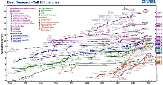
Figure 1 - Plot describing the best efficiencies obtained by all types of solar cells. (This plot is
courtesy of the National Renewable Energy Laboratory, Golden, CO).
1. Introduction
History of Solar Cells
Solar cells are widely used on today’s society, where they play a vital role of ensuring the energetic sustainability of our world. They only require a source of photons that, hopefully, will never cease to exist, the Sun, contrary to the other traditional energy sources that require non-renewable resources, such as fossil fuels or uranium, to generate energy.
Solar cells tend to be assumed as being a recent technology, but they were invented 65 years ago (1954). The first solar cell was silicon based and it was created by Chapin, Fuller, and Pearson at Bell Laboratories in New Jersey [6]. This cell had an efficiency of 6% but, in just 6 years (1960), Hoffman Electronics were able to get the efficiency up to 14% [7]. Since those times, the solar energy industry has increased exponentially through the years and nowadays, it is possible to produce solar cells with efficiencies up to 47% [8].
There are many types of solar cells and they are divided in three generations. The first generation cells are made by crystalline silicon wafers, they can be single crystal (higher efficiency) or multicrystalline (cheaper and easier production) solar cells. This generation still represents around 90% of the photovoltaic devices that currently exists worldwide [9]. The second generation consists of solar cells fabricated with thin film's materials, such as a-Si, CdTe, CIS and CIGS solar cells. They have lower efficiencies than the first generation cells but they are more visually pleasing, can be produced on larger areas and allow more applications on transparent and flexible substrates [10]. The third generation also consists of thin film technology but using organic, flexible and less toxic materials such as polymeric, dye sensitized, nanocrystal and perovskite solar cells [11].
2
Figure 2 - Representation of the energy conversion process of a solar cell [12].
Perovskite solar cells (PSCs) are one of the most promising technologies to be a commercial alternative to the silicon solar cells. PSCs have low processing costs, are composed of abundant raw materials, produce low CO2 emissions and have many remarkable possible applications like using them in building facades or in tandem perovskite−Si architecture as top cells [13]. Since their introduction in 2009, when the higher obtained efficiencies were around 3.8%, this technology witnessed an astonishing evolution and now (2019) the record efficiencies have reached over 25% [14],[15],[16]. Perovskite solar cells (PSCs) have been improving considerably, not only in terms of power conversion efficiency (PCE) but also regarding the device metrics such as the short-circuit current densities (JSC), that have been reaching high values, as well as the fill factor (FF) and their corresponding open-circuit voltages (VOC) values [17]. Therefore, to improve the PSCs efficiencies even more it is necessary to further increase the VOC and FF values by reducing or eliminating any recombination pathways that might occur in the cell [18]. It is also vital for practical application to reduce the cells' production costs, increase their short lifetime, increase their efficiencies on flexible substrates and try to reduce their toxicity (e.g. due to presence of Lead, Pb), although it is lower compared to the Si technology [19].
1.2.1 Perovskite Properties
Perovskite materials follow the general formula ABX3 and adopt a crystal structure arrangement where the ‘A’ and ‘B’ are cations (A is monocation, bigger than the dication B) that coordinate with the ´X´ anion. Normally, A is an organic molecule, such as FA or MA, B is either Sn or Pb and X is a halogen, like I, Cl, Br, or a combination of them. Since it is possible to adjust the material properties by mixing the different integrating elements it is common to achieve different variations of the organometal halide CH3NH3BX3 that can form cuboctahedral and octahedral geometries, whose properties were first described by Weber in 1978 [20], [21], [22], [23]. These perovskite compounds have excellent properties for PV applications such as: (a) strong optical absorption of the visible and near-infrared spectra due to s-p antiboding coupling; (b) low surface recombination rate; (c) harmless grain boundary effects; (d) high electron and hole mobilities and diffusion lengths; (e) high tolerance to structural and shallow
3
point defects; (f) adjustable band-gap; (g) high carrier mobility and lifetime; (h) solution processability [20], [23], [24], [25]. They also exhibit different electronic properties, depending on the specific type of perovskite material, such as superconductivity, piezoelectric, semiconductivity and thermoelectric properties [25], [26], [27].
Figure 3 - Crystal structure of perovskites with the generic ABX3 configuration [25].
Although the perovskite materials have many beneficial properties, they also have some negative aspects like their toxicity caused by the lead, the photocurrent hysteresis observed in current density−voltage (J−V) curves of the cells, poor stability when exposed to high temperatures and illumination and, most importantly, their sensitivity to humidity and moisture which limits, considerably, the lifetime and overall quality of the cells [28]. This occurs because the MA cation is connected to the lead and iodide, by weak hydrogen bonds, which are easily broken or decomposed by water molecules [29]. To avoid these problems, the PSCs are normally fabricated in a glove box, or other highly controlled environment, that can regulate and maintain optimal atmospheric conditions, to enhance the performance and durability of the solar cells. Producing high efficiency PSCs without using these expensive equipment and controlled environments is a remarkable achievement, that represents the reduction of the PSCs manufacturing and selling price [28].
1.2.2 Architecture and Configuration
A perovskite solar cell has a more complex structure compared to a typical solar cell (Figure 2), with some apparent differences in the configuration of its layers as it is an hetero-junction. Normally, PSCs are composed of the following 6 layers: a) Transparent substrate, most commonly a transparent conductive oxide (TCO) coated on glass; b) Semiconductor compact layer, normally made of TiO2 (n-type material which forms a n-i junction that regulates the flow of the electrons), known as the electron transport layer (ETL); 3) Semiconductor mesoporous layer, that acts as a scaffold for the perovskite layer deposition, which limits the hysteresis effects and promotes the motion of the electrons to the compact layer, increasing the carrier-collection efficiency, even if the photon absorption length is higher than the diffusion length of the charge carrier; 4) Active perovskite layer, which absorbs the light and creates the charge separation that leads them to their electrodes; 5) Hole transport layer (HTL), that is composed of a p-type material that acts as an i-p junction that regulates the hole transport mechanism; 6) Metallic electrode contact, normally made of gold, that allows a good bonding with the other layers. The valence band of the HTL must be higher than the perovskite valence
4
achieve a more efficient charge extraction and movement [30], [31], [32], [33].
The conventional n-i-p mesoscopic perovskite solar cell architecture (Figure 3(a)) is not exclusive, there are other variations of this structure. One is the inverted structure (p-i-n), where the layers are deposited in the reverse order of the conventional architecture (n-i-p) (Figure 4(d)). Both of these architectures, n-i-p and p-i-n, can also function without the mesoporous layer, which results in, so called, planar structures (Figure 4(b) and Figure 4(c)). The main differences, that distinguish the mesoscopic from the planar structure, are that the latter eliminates the porous metal oxide framework, which causes the formation of two interfaces between the perovskite materials and the two layers (ETL and HTL) and the thickness of the ETL in both structures (ETL in a planar structure is much thinner compared to one in a mesoscopic structure) [34], [35], [36], [37].
Figure 4 - Schematics of the most used configurations of a perovskite solar cell (PSC): a) n-i-p
mesoscopic, b) n-i-p planar, c) p-i-n planar, d) p-i-n mesoscopic [33].
1.2.3 Device Preparation and Fabrication
After defining the configuration of the PSC, it is necessary to plan the composition and fabrication method of all the layers of the device. The most used deposition method is the spin-coating, when working with small-area (<10 cm2) devices, because it is easy to operate, environmental friendly, cheaper and can achieve better film uniformity, compared to the other alternatives intended for large-area patterning like doctor blade coating, spray pyrolysis, dip-coating, inkjet printing, vacuum sublimation, thermal and chemical evaporation [38], [39], [40], [41], [42].
Firstly, the ETL, has the purpose of extracting and collecting electrons efficiently, so it must be composed of reliable semiconductor electron transport materials like SnO2, ZnO or TiO2. The most preferable material to be used as an ETL material, regardless if it is for a planar or mesoscopic ETL structure, is the TiO2 due to its non-toxicity, chemical stability and favorable optical properties (transparent to the visible radiation, low absorption rate, high refractive index and high transmittance) [43], [44], [45]. These properties accompanied with the high electron transport length, increased electron injection rate, increased carrier lifetime, decreased electron-hole recombination rate and geometrical anti-reflection coating action created by the mesoporous material, makes TiO2 a great ETL material [46], [47]. However, it also has a big disadvantage: it requires the formation of a compact ultra-thin layer that requires high annealing temperature (higher than 400 °C), which prevents the use of some cheap, light
5
and flexible substrates, due to their low melting temperatures, and also requires expensive heating equipment and energy costs [48].
Regarding the perovskite film, it is of extreme importance to optimize this layer in order to dramatically improve the overall quality and performance of the solar cell. This optimization of the perovskite layer can be done by controlling the parameters that influence its quality, crystallinity, energy level (Figure 5), and other morphological and functional properties, such as the deposition method, annealing time and temperature, atmospheric conditions and the perovskite solution processing method [26], [48]. There are many solvents to process the perovskite solution, such as N, N-dimethylformamide (DMF), Dimethyl Sulfoxide (DMSO) or γ-butyrolactone (GBL). The GBL is normally a better solvent for I-based perovskites due to its high solubility and necessity lower temperatures, while DMF and DMSO are most advised for the Br-based ones, although they also perform well as I-based perovskites solvents. DMF and DMSO strongly coordinate Pb2+, whereas GBL leads to the formation of clusters in the solution due to the weak interactions that occur between lead ions and the GBL molecules. When using DMF or GBL as solvents, the interaction of MAI with PbI2 is slower, allowing a good crystallization of the MAPbI3 crystals, when the solvents are evaporating [50], [51], [52].
The HTL, whose job is to selectively collect the holes and transport them to the metallic electrode, prevents the damage of the perovskite layer, by separating it from the metallic contacts and also minimizes the charge recombination that would happen on that interface (perovskite layer – metallic contacts) otherwise [50]. The most used HTL material in PSCs, according to the literature, and the one that achieves higher efficiencies is the Spiro-OMeTAD [41], [53]. However, this material has some drawbacks such as its high production cost [1], quick degradation with environmental conditions, low conductivity and hole mobility in its pristine form, and also causes self-aggregation when deposited [54]. One good alternative is the Copper(I) Thiocyanate (CuSCN), an inexpensive [2] and abundant metal halide of singly ionized copper that has a well-aligned work function, high hole mobility, good thermal stability, suitable energy levels and it is not easily degraded [55], [56], [57], [58].
7
2. Methods and Materials
Device Fabrication
The solar cells’ fabrication process consisted firstly by the etching of the fluorine-doped tin oxide (FTO) from the sides of the substrate, the cleaning of the glass substrates, the deposition of the electron transport layer (ETL), active layer (perovskite) and hole transport layer (HTL), and finally the gold contacts deposition. All the depositions, except the last one, were carried out via spin-coating (as presented in Figure 6) and the whole fabrication process was performed without a glove box, therefore there was no control or information of the temperature and moisture conditions. It is also important to refer that before each deposition, the unetched edges of the substrate were covered with kapton tape.Also, all the information regarding the reagents used in this work is presented in Table 11 from section B of Appendices.
Figure 6 - Perovskite solar cell (PSC) layers deposition steps and corresponding annealing
conditions. This work employed the conventional n-i-p superstrate configuration (Figure 4a).
2.1.1 Substrate Preparation and ETL deposition
The FTO coated glass substrates (100 mm x 100 mm x 2.2 mm, 13 Ω/sq, 82-84.5% of transmittance), cut into 2.5 cm x 2.5 cm, were etched with zinc powder, HCl + water solution and cotton buds. The substrates were then cleaned in an ultrasonic bath of detergent, ionized water (2 baths), acetone and ethanol, in this order for 15 minutes each, after which were dried with nitrogen flow and clean room paper and placed in the UV ozone system during 15 minutes for enhanced cleaning treatment. Regarding the ETL, it was firstly deposited the compact TiO2 layer (c.TiO2), whose solution is described in section C.1 of Appendices. 120 µL of the c.TiO2 solution were dropped on the substrate and spun at 4000 rpm for 35 s with a ramp of 2000 rpm/s. The substrate was then dried at 120 °C for 10 minutes on the hot plate and then annealed in a furnace at 500°C for 30 minutes. After the substrate cools down, it is deposited the mesoporous TiO2 (mp.TiO2) layer, by dropping 120 µL of the mp.TiO2 solution (described in Section C.1 of Appendices) on the substrate which is then spun at 4000 rpm with a ramp of 2000 rpm/s for 20 s and posteriorly dried for 10 min at 100 °C and annealed in the furnace for 30 min at 450 °C. It was also tested to perform a Li+ treatment of the mp.TiO2 layer by depositing 150 µL, of LI-TFSI solution in acetonitrile (10mg/mL), at 3000 rpm with a ramp of 2000 rpm/s for 20 s, which was later annealed at 450 °C for more 30 min.
8
2.1.2 Perovskite Solution Preparation and Deposition
Before starting the perovskite layer deposition, the solutions (described in section C.2 of Appendices) were filtered through a 0.22 µm syringe filter and heated at 65 °C, as well as the substrate where it will be done the deposition. 100 µL of one of the solutions are then deposited and spin coated in a two-steps program at 1000 rpm for 10 s with a 500 rpm/s ramp and 5000 rpm, with a 2000 rpm/s ramp, for 20 s. When executing the second step, a certain volume (80 µL, 130 µL or 200 µL)) of toluene is poured on the substrate when there are 10 s left to the end of the program. After this process, the substrate is annealed at a defined temperature (65º, 110 °C, 125 °C) on the hot plate during a certain duration (3, 10 or 20 min).
2.1.3 HTL and Top Electrode Depositions
For the HTL, three solutions of copper(I) thiocyanate (CuSCN) powder dissolved in diethyl sulfide, with different concentrations (20 mg/mL, 35 mg/mL and 50 mg/mL) were filtered through a 0.22 µm syringe filter, and different volumes (35 µL, 50 µL or 80 µL) were deposited on the substrates by drop casting method, 2 seconds after the spinning program of 25 s at 3000 rpm with a 1000 rpm/s ramp started, and were then annealed at 65 °C for 2 min on the hot plate. Finally, the substrates are covered by acetate masks, produced by LASER (Universal LASER Systems) and the gold electrodes, with thicknesses around 100 nm and active areas dependent of the masks structure, are deposited by electron-beam evaporation under high vacuum, in a clean room.
Characterization
2.2.1 SEM-EDS
The top-surface and morphology images were obtained by Tabletop Microscope TM3030 Plus + Quantax 70 SEM and the cross-sectional images were examined by scanning electron microscopy (SEM) using a Carl Zeiss Auriga crossbeam (SEM-FIB) workstation instrument equipped with an Oxfotd Intruments Aztec X-ray energy dispersive spectrometer.
2.2.2 XRD
The crystal structures characterization of the substrates was done with X-ray diffraction (XRD) by using a PANalytical X’Pert Pro X-ray diffractometer in Bragg-Brentano geometry, with a monochromatic radiation source of Cu-Kα (λ=1.5406 Å).
2.2.3 UV-Vis-NIR Spectroscopy
The reflectance and total transmittance of all the samples were obtained by using a UV-Vis-NIR - Perkin Elmer Lambda 950 spectrophotometer with a ISR-260 integrating sphere within a wavelength range of 300-1200 nm.
2.2.4 Opto-electrical Characterization.
The I-V curves of the cells were measured by VeraSol-2 LED Class AAA Solar Simulator from Oriel, using forward scan (ISC to VOC) under ambient conditions at RT and with illumination intensity of one Sun (1 kW/m2).
9
3. Results and Discussion
This chapter consists in the presentation and discussion of the results obtained from the characterization studies performed on the produced solar cells. The opto-electrical characterization was the most abundantly performed one, to assess the performance of the perovskite solar cells (PSCs), but other characterization tools were also employed for morphological, optical and structural analyses. The devices that were opto-electrically characterized were slightly different from those used for the other types of characterizations because, although being fabricated within the same conditions and having the same composition and structure, their rear side was coated with the gold electrode, thus preventing the cells to be used for some of the other measurements.
This chapter is divided into sections that analyse the influence of several parameters of the three main layers (electron transport layer, perovskite layer and hole transport layer) on the overall performance of a PSC with conventional n-i-p superstrate configuration (Figure 4a), giving special focus to the perovskite layer and the HTL. Through the study of these parameters, a PSC with an in-house record PCE (power conversion efficiency) was obtained, and its characterization and performance results are exhibited in this chapter, as well as a final study that regards the effect of time on the degradation of the PSCs.
ETL Layer Composition
This section correlates the composition of the ETL with the performance of the PSCs. Preferably, the ETL should have a high transmittance to facilitate the passage of light that goes through it, reaching the active layer more effectively. In Figure 7 b), it is possible to see that the transmittance of the substrate with mesoporous TiO2 is higher than the one with only compact TiO2 layer. This happens due to the mesoporous layer acting as a geometrical anti-reflective coating on top of the compact layer, which reduces its reflectance (as shown on the same figure) and enhances its transmittance, while maintaining its low absorbance, observed in Figure 7 a), as it is desirable for the ETL [59],[60]. The mesoporous layer also works as a photonic structure that minimizes the diffraction between the TiO2 and the air, because its refractive index is lower than the one of the compact layer by itself (1.623 of the mp.TiO2 vs 1.789 of the c.TiO2) [61], which also contributes to the reduction of the total reflectance and corresponding increase of the total transmittance. Besides, the incorporation of the mesoporous TiO2 also provides a wider surface-area connection between the ETL and the active layer, resulting in a more homogeneous and continuous flow of light that reaches the perovskite layer.
10
Figure 7 - a) Absorbance spectrum of only the ETL deposited over FTO, with only compact TiO2
layer (blue) and also with Mesoporous TiO2 over it (red), as well as the representation of the ETL architecture; b) Transmittance and Reflectance spectra of the same ETL.
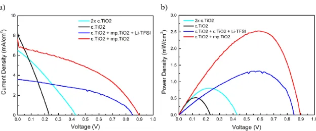
An opto-electrical characterization of four cells with different ETL configurations was performed, with only a c.TiO2 layer, with two c.TiO2 layers, with the classic mesoscopic ETL (c.TiO2 layer + mp.TiO2 layer) and with the Li+ doping (c.TiO2 layer + mp.TiO2 layer + Li-TFSI), because this last ETL composition achieved the best results in the latest M.Sc. work [3]. The results were extracted from the I-V curves which already exhibited the open circuit voltage (VOC) and the short-circuit current density (JSC) and, also, the equations presented in section A of Appendices were used to obtain the fill factor (FF), shunt resistance (RSH), series resistance (RS) and power conversion efficiency (PCE) of the cells. As can be seen, in Figure 8 and in Table 1, the cell that achieved the highest PCE value was the one who had a mesoscopic structure, whose ETL was composed only by a compact and mesoporous TiO2 layer. This led to the conclusion that a mesoscopic ETL, without Li+ treatment, is more reliable and achieves higher efficiencies so for all the following fabricated cells, analysed in this thesis, their ETLs were always deposited with this structure.
Figure 8 - a) J-V and b) P-V measurements of the four best solar cells with different ETL, which
are composed of: 1x c.TiO2 (black), 2x c.TiO2 (cyan), c.TiO2 + mp.TiO2 (red) and c.TiO2 + mp.TiO2 + Li-TFSI (blue).
11
Table 1 – Electrical performance values (VOC, Jsc, FF, RSH, RS and PCE) for the best devices
(illustrated in Figure 8) obtained from a batch of 28 samples. The active area of the devices is 0.12 cm2.
Perovskite Layer
The perovskite absorber layer is the one with most impact on the overall performance of the device, so, it is essential to obtain optimal conditions and quality for this layer. In this work, many studies regarding the perovskite layer were performed, many different perovskite solutions from the literature were prepared and tested, and several production parameters were compared and analysed. The perovskite solution that achieved the best results, on the initial trials, was the one described in Appendix C.2. Therefore, it was the solution used for all the studies presented in this thesis.
To analyse the influence of the production parameters on the quality of the perovskite layer, as well as on the overall performance of the devices, opto-electrical, optical, morphological and structural characterization were performed, and the results were considered. Due to this study, it was possible to verify a continuous improvement of the devices performance, as can be seen by the results and conclusions described along this section.
3.2.1 Effect of MAPbI3 solution concentration
The perovskite solution concentration is a parameter that has not been studied much in the latest works, but it is a fundamental parameter to achieve a uniform perovskite layer with great quality. So, in this section, the effect of the MAPbI3 solution concentration is deeply studied and it is observed the impact that it has on the performance of the devices.
Three solution concentrations (0.8 M, 1 M and 1.2 M) are investigated in this section, through the analysis of the optp-electrical, optical and structural characterization of different devices, which are composed by their respective solutions.
The optical spectra represented in Figure 9 show an unexpected result for the absorbance values of the devices. The 1.2 M perovskite concentration cell exhibits higher absorbance values, followed by the 0.8 M and the 1 M cells, by this order, which is contrary to what was expected, because as the concentration of the perovskite layer rises there should be a reduction of the light passing through the perovskite layer, which would decrease the transmittance values and increase the absorbance values. This is not verified in this case because the 0.8 M concentration sample exhibited higher absorbance values than the 1 M sample. Besides, as will be later described in this section, the cell that achieved a higher efficiency was the one with 1 M concentration. This incongruity can be explained by the fabrication and characterization procedure adopted in this work, where some cells with similar configurations
ETL Configuration VOC (V) Jsc (mA/cm2) FF RSH (Ω) RS (Ω) PCE (%)
1 c.TiO2 layer 0.23 8.25 0.27 80.97 87.40 0.52
2 c.TiO2 layers 0.43 6.51 0.29 822.62 390.98 0.81
c.TiO2 + mp.TiO2 0.90 6.86 0.41 2657.19 365.16 2.52
c.TiO2 + mp.TiO2 +
12
and composition, produced in identical conditions, were used only for the opto-electrical characterization, after the gold deposition, while the similar cells, without gold contacts, were used for the other characterization techniques (structural and optical). Even though the cells were produced in identical conditions, in perovskite technology it is quite difficult to achieve two exact twin cells, which explains these incongruities. Despite the differences between the absorbance values, the 1.2 M and 1 M samples have a similar band gap of 1.59 eV, while the 0.8 M has a lower band gap of 1.56 eV (values obtained by the Tauc plot represented in Figure 32 a) in section D of Appendices.
Figure 9 - a) Absorbance, b) Transmittance and reflectance spectra of three devices, which
structure is illustrated on a), that are composed of perovskite layers that have different solution concentrations: 0.8 M (blue), 1 M (red) and 1.2 M (black).
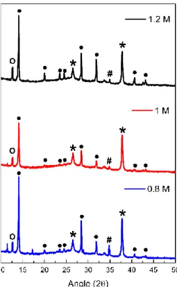
The XRD results of the three devices (Figure 10) exhibit the (110), (112), (211), (202), (220), (310), (224) and (314) planes at an angle 2θ of 14.20º, 19.97º, 23.61º, 24.5º, 28.46º, 31.87º, 40.60º and 43.14º respectively, which denotes the presence of the tetragonal phase of the MAPbI3, marked with full circle on Figure 10 [62], [63], [64], [65]. It is also noticeable the existence of the PbI2 phase peak, due to its relatively low solubility in GBL, at an angle 2θ of 12.67º, the FTO diffraction peaks at an angle 2θ of 26.52º and 37.75º, and the CuSCN peak at an angle 2θ of 34.85º, that are pointed out, in Figure 10, with an open circle, asterisk and cardinal, respectively [66], [67], [68], [69]. Comparing the three XRD graphs, it is observed that the MAPbI3 tetragonal phase peaks for the 0.8 M and 1.2 M are more intense than for the 1 M sample, which is a sign that these two substrates have a higher crystallinity in comparison to the 1 M. These results together with the absorbance spectrum presented in Figure 9 a), go along with the litterature, that relates higher crystallinity with higher absorbance values.
13
Figure 10 - XRD results of the samples (all layers deposited except gold) fabricated with different
perovskite concentrations: 0.8 M (blue), 1 M (red) and 1.2 M (black). Tetragonal perovskite crystal structure peaks marked with full circle; PbI2 peaks marked with open circle; FTO peaks marked with asterisk; CuSCN peaks marked with cardinal.
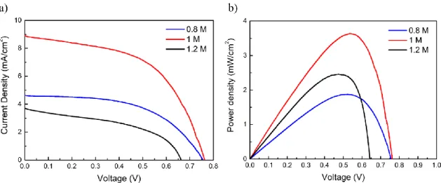
The results obtained by the opto-electrical characterization measurements for this study are presented in Figure 11 by the J-V and P-V (power-voltage) curves extracted from the I-V curves of the PSCs. Table 2 describes all the electrical parameters of the PSCs, namely the open circuit voltage (VOC), short circuit current density (JSC), fill factor (FF), shunt resistance (RSH), series resistance (RS) and power conversion efficiency (PCE). By analysing these results, it is possible to observe a contradiction to the previous optical and structural analysis that pointed out the 1 M concentration substrate as having the lowest absorbance and crystallinity values. This is because the 1 M concentration cell achieved the best performance values, as can be seen by its PCE of 3.63%, which is more than 1% higher than that of the 1.2 M, and around two times higher than the one of the 0.8 M perovskite concentration. So, for all the following studies on this work, the 1 M perovskite solution concentration was used.
14
Figure 11 - a) J-V and b) P-V curves of the three best solar cells with different perovskite layer
concentrations: 0.8 M (blue), 1M (red) and 1.2 M (black).
Table 2 – Electrical performance values for the best devices (illustrated in Figure 11) obtained
from a batch of 40 samples. The active area of the devices is 0.12 cm2.
3.2.2 Effect of the toluene (anti-solvent) volume
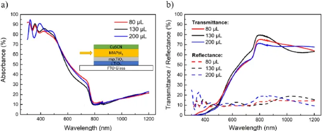
The toluene deposition during the spinning of the perovskite solution is a necessary step to ensure the washing of the GBL (perovskite solution solvent), that has a high boiling point (204 ºC) which makes it impossible to evaporate during the annealing process [70]. This technique is an effective way to achieve uniform crystallization, controlled morphology and high reproducibility of the perovskite solar cells. The most important parameter for tuning is the amount of washing solvent deposited, because it affects the particle size distribution of the perovskite which has a great influence in the interconnections between the crystal grains [71]. Therefore, taking into account that all the samples have an area of 2.5 cm x 2.5 cm and the perovskite solution volume deposited is always 100 µL, the effect of the volume of anti-solvent deposited, during the perovskite layer spin-coating procedure, was tested by drop-casting three chosen volumes of toluene (80 µL, 130 µL and 200 µL - adequate for samples with these characteristics) and then analysing the results of opto-electrical, morphological and optical characterizations of the produced devices.
Concentration VOC (V) Jsc (mA/cm2) FF RSH (Ω) RS (Ω) PCE (%)
0.8 M 0.75 4.61 0.54 25167.21 472.91 1.87
1 M 0.76 8.87 0.54 5217.17 241.02 3.63
15
Figure 12 - a) Absorbance, b) Transmittance and reflectance spectra of three samples, whose
structures are illustrated in the inset in a), that are composed of perovskite layers that were washed by toluene volumes of: 80 μL (red), 130 μL (black) and 200 μL (blue).
The three volumes of toluene resulted in cells with similar band gaps of 1.59 eV (value obtained by the Tauc plot represented in Figure 32 b) from section D of Appendices, and with close absorbance values , for the 80 µL and 200 µL that are relatively higher in comparison with the 130 µL ones, as shown in Figure 12 a). These results can be compared with the opto-electrical characterization results, presented in Figure 14 and summarized in Table 3, where we observe that the highest efficiency (PCE) corresponds to the 80 uL sample, which also has the highest absorbance value, followed by the 200 uL and the 130 uL, by this order. This leads to the conclusion that volumes of toluene deposition around 80 µL provide high absorption values which seem to be linked with better performances of the cells.
The influence of the volume of toluene deposited was also examined by the top-view SEM images represented in Figure 13, where it is possible to observe perovskite crystal structures with irregular shapes (some resembling a flower-like morphology), rough edges and high porosity that sometimes happen for perovskite solutions containing GBL as solvent [72]. It is also noticeable that the deposition of higher volumes of toluene seems to result in a wider disconnection of these crystals, creating larger gaps between them due to the washing of higher amounts of solvent, which contributes to the deagglomeration of the perovskite crystal structure resulting in a larger uncovered area beneath it [73].
Figure 13 - Top-view SEM images of cells with perovskite layers washed by different toluene
volumes: a) 80 μL, b) 130 μL, c) 200 μL. The samples are composed of all the layers with the exception of the gold contacts.
16
The results obtained by the opto-electrical characterization measurements for this study are presented in Figure 14 and in Table 3. In Figure 14 it is shown the J-V and P-V curves extracted from the I-V curves of the best contacts of the PSCs produced with different toluene washing volumes. Comparing the performance values of the three cells presented in Table 3, it is noticeable that the best cell is the one where 80 µL of toluene were dropped. This cell exhibits a VOC of 0.79 V, JSC of 11.32 mA/cm2, FF of 0.52, and PCE of 4.64%, which is relatively higher than the other cells. Although the FF value is higher for the 200 µL cell, the 80 µL has a much higher JSC and has the best PCE of the three. Therefore, as a result of this study, it is admitted that a toluene volume of 80 µL is ideal for better performances and electrical properties of the PSCs. As such, all the following studies on this work were performed using 80 µL of toluene as the chosen anti-solvent volume.
Figure 14 - a) J-V and b) P-V curves of the three best solar cells with different volumes of toluene
washing deposited: 80 μL (red), 130 μL (black) and 200 μL (blue).
Table 3 - Electrical performance values for the best devices (illustrated in Figure 14) obtained
from a batch of 30 samples. The active area of the devices is 0.12 cm2.
Toluene Volume VOC (V) Jsc (mA/cm 2) FF R SH (Ω) RS (Ω) PCE (%) 80 μL 0.79 11.32 0.52 2612.94 129.29 4.64 130 μL 0.76 10.31 0.48 3440.99 209.62 3.75 200 μL 0.79 9.26 0.55 2389.70 83.33 4.03
17
3.2.3 Effect of the Annealing Temperature of the Perovskite Layer
An important factor that highly influences the quality of the perovskite layer and the performance results of its corresponding cell, is the annealing temperature. This fabrication parameter also has a big impact in the device morphology and optical properties, as it will be observed by the studies performed in this section. According to the literature, PSCs produced with higher annealing temperatures exhibit faster degradation and lower lifetime, while the ones annealed with temperatures below a certain threshold (around 54ºC), do not crystalize and remain with a yellow coloration [74]. So, the temperatures chosen to perform this study were 65ºC (it is the pre-heating temperature of the substrates and, also the stirring temperature of the perovskite solution), 110ºC, which according to the literature is the temperature that provides higher efficiencies for this kind of perovskite [75], and 125ºC, that is a relatively high temperature which might cause a decay of its device performance values.
In this study, as can be observed in the plots represented in Figure 15, the sample that obtained a higher absorbance was the one annealed at 110ºC, but its absorbance values do not differentiate much from the ones of the sample annealed at 125ºC. On the other hand, the sample annealed at 65ºC exhibited a much lower absorbance and much higher transmittance values than its competitors, which might be related to a weak crystallization of the perovskite layer, due to the low temperature, which causes the light to pass through it much more easily, which is undesirable for PSCs. Despite the existing disparity between the absorbance values of the samples, they all have the same band gap value of 1.59 eV, as shown in Figure 32 c) from section D of Appendices.
Figure 15 - a) Absorbance, b) Transmittance and reflectance spectra of three samples, which
structures are illustrated on a), that are composed of perovskite layers annealed at a temperature of: 65ºC (black), 110ºC (red) and 125ºC (blue).
These three annealing temperatures also resulted in films with distinct surface morphologies, as can be seen in Figure 16. The SEM image of the sample annealed at 65ºC, Figure 16 a), reveals an inhomogeneous film with some zones where a full crystallization of the perovskite did not occur, probably due to the lack of enough temperature. For the annealing at 110ºC, Figure 16 b), a highly homogeneous film with regular grain size is visible, whereas for the sample annealed at 125ºC, Figure 16 c), its SEM image exhibits an irregular grain size and an inhomogeneous film with many vacancies, which might be indicative that the annealing
18
temperature used (125ºC) is close to the maximum threshold that the perovskite can sustain before starting to occur the degradation of its organic compound (MAI).
Figure 16 - Top-view SEM images of samples with different perovskite layer annealing
temperatures: a) 65ºC, b) 110ºC, c) 125ºC . The annealing process of the perovskite layer had a duration of 10 minutes for all three samples. All the PSC layers were deposited on these samples with the exception of the gold contacts.
The J-V and P-V curves extracted from the opto-electrical characterization results of this study are shown in Figure 16 and the electrical parameters of the cells are described in Table 4. It is visible that the best cell of this batch, in terms of electrical performance, is the one that had its perovskite layer annealed at 110ºC, as can be seen by its PCE of 5.32%, VOC of 0.70 V, JSC of 11.84 mA/cm2 and FF of 0.65. The PCE value is superior to the one obtained for the cell annealed at 125ºC (4.39%) and even more superior compared to the cell annealed at 65ºC (3.63%). Although there is a considerable difference of efficiencies, the cells have almost identical VOC and FF values, which means that the parameter more affected by the annealing temperature was the JSC. Besides, it is also concluded by the analysis of these results that it is more difficult to achieve PSCs with high electrical performance if the annealing temperature is low rather than higher temperatures (the PCE of the 125ºC cell is considerably higher than the 65ºC cell), which might be related to an incomplete crystallization of the perovskite layer.
Figure 17 - a) J-V and b) P-V curves of the three best solar cells of which perovskite layer was
19
Table 4 - Electrical performance values for the best devices (illustrated in Figure 17) obtained from a
batch of 30 samples. The active area of the devices is 0.12 cm2.
3.2.4 Effect of the Annealing Time of the Perovskite Layer
According to the literature, the annealing time influences the crystallization and morphology of the perovskite films, and it is a interesting parameter to study because it provides information needed to optimize the production costs and time of the PSCs. It was chosen a short annealing time of 3 minutes to verify if it would be enough for the crystallization of the perovskite structure, an annealing time of 10 minutes that was considered the best one in many works that used this perovskite material (MAPbI3) and also a longer annealing duration of 20 minutes to notice if it would start causing the degradation of the perovskite layer, due to overheating [76]. During the annealing step, it was not visible any difference at the naked eye between the cells annealed for 3 minutes and the ones annealed for 10 minutes because the crystallization of the perovskite layer was almost instantaneous (transition from a yellow to a brown coloration) but for the cell that was annealed for 20 minutes it was possible to observe a slight change of color to a more yellowish tone, on the last 2 minutes of annealing, that might be a signal of some degradation of the perovskite layer due to overheating.
Figure 18 - a) Absorbance, b) Transmittance and reflectance spectra of three samples, which
structures are illustrated on a), that are composed of perovskite layers annealed at a temperature of 110ºC during: 3 minutes (blue), 10 minutes (red) and 20 minutes (black).
An optical characterization study was performed and, as can be observed in the spectra represented in Figure 18, the sample that portrayed the best optical properties for a PSC (higher absorbance and low lower transmittance values) was the one annealed during 10 minutes, followed by the cell annealed for 20 minutes and the cell annealed during 3 minutes, by this order, which suggests that excessively short or long annealing times might not be advisable for the perovskite layer fabrication, as was referred before. Despite these differences on the optical
Temperature VOC (V) Jsc (mA/cm2) FF RSH (Ω) RS (Ω) PCE (%)
65ºC 0.68 8.26 0.65 5582.03 64.60 3.63
110ºC 0.70 11.84 0.65 3371.72 59.01 5.32
20
spectra, the cells annealed during 3 and 10 minutes obtained a similar band gap value of 1.59 eV whereas the cell annealed for 20 minutes presented a slightly lower band gap value of 1.58 eV, as in Figure 32 d) from section D of Appendices.
The results of the opto-electrical measurements are shown in Figure 19 and in Table 5, where it is possible to visualize the J-V and P-V curves extracted from the I-V results, and the values of the most important electrical parameters of the cells. The cell that exhibited the best performance values was annealed for 10 minutes, achieving a high PCE of 8.09%, a VOC of 0.85 V, a JSC of 14.75 mA/cm2 and FF of 0.64. These values are much superior compared to the ones of its other two competitors, especially the VOC value (0.14 V higher than the 20 minutes’ cell and 0.16 V higher than the 3 minutes’ cell), which is the main factor of such a disparity regarding the PCE values obtained. The cell that achieved the lowest PCE value, out of the three, was the cell annealed during 20 minutes, which is probably a result of overheating which might have triggered the decomposition of the perovskite crystal structure, lowering the stability of the cell as well as its lifetime. Therefore, as was expected and pointed out in the literature, the optimal annealing time to achieve better electrical performance values, for annealing temperatures close to 110ºC, is around the 10 minutes mark, because it is long enough to allow the crystallization of the perovskite layer but not to overheat the film which would cause the degradation of the perovskite crystal structure, and the reduction of the performance values of the cell.
Figure 19 - a) J-V and b) P-V curves for the three best cells that had their perovskite layers
annealed for different durations: 3 minutes (blue), 10 minutes (red) and 20 minutes (black).
Table 5 - Electrical performance values for the best devices (illustrated in Figure 19) obtained
from a batch of 40 samples. The active area of the devices is 0.12 cm2.
Duration VOC (V) Jsc (mA/cm2) FF RSH (Ω) RS (Ω) PCE (%)
3 min 0.69 12.71 0.70 4849.93 56.17 6.10
10 min 0.85 14.75 0.64 6670.95 46.14 8.09
![Figure 2 - Representation of the energy conversion process of a solar cell [12].](https://thumb-eu.123doks.com/thumbv2/123dok_br/18180145.874431/28.893.298.653.124.415/figure-representation-energy-conversion-process-solar-cell.webp)
![Figure 3 - Crystal structure of perovskites with the generic ABX3 configuration [25].](https://thumb-eu.123doks.com/thumbv2/123dok_br/18180145.874431/29.893.324.619.237.464/figure-crystal-structure-perovskites-generic-abx-configuration.webp)
![Figure 4 - Schematics of the most used configurations of a perovskite solar cell (PSC): a) n-i-p mesoscopic, b) n-i-p planar, c) p-i-n planar, d) p-i-n mesoscopic [33]](https://thumb-eu.123doks.com/thumbv2/123dok_br/18180145.874431/30.893.181.717.406.623/figure-schematics-configurations-perovskite-mesoscopic-planar-planar-mesoscopic.webp)
![Figure 5 - Diagram of the energy level alignment of PSC layers used in this work (Based on [41])](https://thumb-eu.123doks.com/thumbv2/123dok_br/18180145.874431/31.893.261.646.744.1035/figure-diagram-energy-level-alignment-psc-layers-based.webp)