F
ACULDADE DEE
NGENHARIA DAU
NIVERSIDADE DOP
ORTOAn Integrated Instrumentation
Amplifier for Myoelectric Signals
Henrique Rodrigues de Castro Mendes Martins
Mestrado Integrado em Engenharia Eletrotécnica e de Computadores Supervisor: Vitor Grade Tavares (PhD)
c
c
Resumo
Nas décadas passadas, o setor da eletrónica evoluiu exponencialmente. No nosso dia a dia a eletrónica está presente em tudo, nos nossos carros, e até em algumas das nossas roupas. A verdade é que os desenvolvimentos nesse setor aumentaram a qualidade de vida do Homem. No caso de algumas doenças, apenas com o auxílio de sistemas eletrónicos é possível realizar diagnósticos e tratamentos apropriados. Problemas do foro muscular e de movimento são uma vasta área na qual a eletrónica teve grande influência na ajuda a lidar e a tratar essas doenças. A eletrónica moderna permite uma melhor visão do que se passa ao nivel do músculo. Com instrumentação de grande precisão é possivel obter o sinal gerado pelas fibras das membranas musculares, o sinal miográfico. Os sinais miográficos são sinais muito específicos; eles são formados por variações fisiológicas nas fibras das membranas musculares. A medição e o processamento destes sinais é de grande importância, dado que eles permitem olhar diretamente para o músculo. Isto é uma análise importante que precisa de ser feita para :
• Ajudar na tomada de decisão antes/após da cirurgia; • Permitir a medição do desempenho muscular; • Ajudar no processo de reabilitação;
Estes são apenas alguns exemplos daquilo que é possível atingir investindo na investigação e desenvolvimento de sistemas aplicados a esta área em específico. Com isso em mente, a necessi-dade de um sistema que meça e processe tais sinais surge. No entanto, alta precisão e um elevado CMRR têm de ser assegurados, fazendo assim o amplificador de instrumentação uma escolha ób-via para a amplificação destes sinais. Esta tese apresenta o desenho e o desenvolvimento de uma nova topologia para um amplificador de instrumentação baseado na topologia Fully Balanced Dif-ferencial Difference Amplifier (FBDDA). O amplificador atinge um CMRR muito elevado de 122 dB, um ruído integrado de 2µV na gama de 10 Hz a 300 Hz e um offset inferior a 1 mV. Para além disto, ele atinge muito boa estabilidade e boas caraterísticas em geral, assegurando que o espectro de aplicações para o amplificador é muito mais largo.
Abstract
In the past decades, the electronics sector has evolved exponentially. In our everyday electronics is everywhere, in our cars, in our houses and even in some of our clothes. Truth is, the developments in that sector have increased the quality of life of the average Man. In the case of some diseases, only with the aid of electronic systems proper diagnosis and treatments can be made. Muscular and movement related problems are a wide area in which electronics have a great influence in dealing with such diseases. Modern electronics allows us to take a better look at what is going on at the muscle level. With great precision instrumentation we can obtain the signal generated by muscle fiber membranes, the Myographic signal. Myographic signals are a very specific type of signals; they are formed by physiological variations in the state of muscle fibre membranes [1]. The measuring and processing of these signals is of great importance, since they allow looking directly into the muscle [1]. This is an important analysis that needs to be done to:
• Help in decision making both before/after surgery; • Allow measurement of muscular performance; • Aid in the rehabilitation process;
These are just a few examples of what we can achieve investing in the research and develop-ment of electronic systems applied to this specific area. With that in mind, the need for a system that can measure and process such signals arises. However, high precision and a high CMRR must be ensured, thus making the instrumentation amplifier an obvious choice for the amplification of these signals. This thesis presents the design and development of a novel topology for an instru-mentation amplifier based on the Fully Balanced Differencial Difference Amplifier (FBDDA).It achieves a very high CMRR of 122 dB, an integrated noise of 2 µV over the range of 10 Hz to 300 Hz, an offset lower than 1 mV. Beside this, it achieves very good stability and overall good characteristics, assuring that its applications domain is much broader.
Acknowledgements
I would like to thank my parents and my brothers for all the support they’ve given me, throughout all these years. Without their sacrifice, I find it hard to believe that I would be where I am at this moment.
In the same regard, I would also like to thank Marta Galvão for all her support, and all the inspiration she has given me. Her constant support made the passing of obstacles a much easier task.
To my friends - Bruno, Romano and Cristina - goes a big thank you as well, for putting up with me all these years, and making my academic life a much better one.
Last but not least, I would like to thank my mentor, Prof. Vitor Grade Tavares for always having an answer ready for every question, and an advice when I needed it. His help greatly influenced my work, and for the better.
Henrique Martins
“The richest man is not he who has the most, but he who needs the least.”
Unknown Author
Contents
1 Introduction 1
1.1 Problem Presentation and Challenges . . . 1
1.2 Motivation . . . 2
1.3 Objectives . . . 2
1.4 Structure of the Document . . . 2
2 Theoretical Background 5 2.1 Myoelectric signals . . . 5
2.1.1 What are they? . . . 5
2.1.2 Obtaining and measuring . . . 5
2.1.3 Applications . . . 5
2.2 Noise . . . 6
2.2.1 Thermal Noise . . . 6
2.2.2 Flicker Noise . . . 7
2.2.3 Noise in Differential Pairs . . . 7
2.3 Amplifiers . . . 8
2.3.1 Fully Differential amplifiers . . . 8
2.3.2 Differential pair with load resistors . . . 9
2.3.3 Common-mode Response . . . 10
2.3.4 CMOS Differential Pair . . . 11
2.3.5 Stability and Frequency Compensation . . . 14
2.3.6 Common-mode Feedback . . . 15
2.3.7 Class Type of Amplifiers . . . 19
2.3.8 Instrumentation Amplifiers . . . 21
3 Bibliographic Review 23 3.1 Gm variation in rail-to-rail input stage . . . 23
3.1.1 Dc shifting circuit to obtain overlapped transition regions . . . 24
3.1.2 Current Summing Technique . . . 25
3.1.3 Gm Control Through the Use of an Electronic Zener . . . 26
3.1.4 Comparative Analysis . . . 27
3.2 Instrumentation Amplifiers Topologies . . . 27
3.2.1 The Fully Balanced Differential Difference Amplifier (FBDDA) . . . 27
3.2.2 Pseudo-Differential Amplifiers (PDA) . . . 30
3.2.3 Chopper-Stabilized Amplifiers . . . 31
3.2.4 Comparative Analysis . . . 31 ix
x CONTENTS 4 Development of the Instrumentation Amplifier 33
4.1 Input Stage . . . 34
4.2 Gain stage and Output Stage . . . 36
4.3 CMFB . . . 39
5 Simulation and Results 43 5.1 Characterization of the amplifier . . . 43
5.1.1 Discussion of the Results . . . 46
5.1.2 Layout . . . 47
6 Conclusions and Future Work 51 6.1 Conclusions . . . 51
6.2 Future Work . . . 51
A Expressions and simulation setups 53 A.1 Expressions and Calculations . . . 53
A.1.1 Gain Expression for the novel instrumentation amplifier . . . 53
A.1.2 Pole and zero Locations . . . 53
A.2 Simulation Setups . . . 54
A.2.1 Input and Output Swing . . . 54
A.2.2 Minimum Load . . . 54
A.2.3 Integrated Noise . . . 54
A.2.4 Harmonic Distortion . . . 54
A.2.5 PSRR and CMRR . . . 54
A.2.6 Power Consumption . . . 54
B Overview of Single Stage Amplifiers 55 B.1 Basic transistor configurations . . . 55
B.1.1 Common-source configuration . . . 55
B.1.2 Source-follower configuration . . . 56
B.1.3 Common-gate configuration . . . 57
List of Figures
2.1 Applications . . . 6
2.2 Differential pair modelled with noise sources . . . 7
2.3 Basic Differential pair . . . 9
2.4 Basic Differential pair with common mode input . . . 10
2.5 Basic Differential pair with CMOS active load . . . 11
2.6 Differential pair with cascoding . . . 12
2.7 Differential pair with current source load . . . 12
2.8 Differential pair equivalent half circuit . . . 13
2.9 Differential pair with current source load . . . 13
2.10 Differential pair with mirror pole representation . . . 14
2.11 Two-stage operational amplifier . . . 15
2.12 Differential pair with inputs shorted to outputs . . . 16
2.13 Common-mode feedback with resistive sensing . . . 17
2.14 Common-mode feedback with source followers . . . 18
2.15 Common-mode feedback with MOSFETs operating in deep triode region . . . . 18
2.16 Sensing and controlling the output CM level . . . 19
2.17 Typical Instrumentation Amplifier . . . 22
3.1 Gm variation along the supply rail. . . 23
3.2 Gmn vs Gmp along the supply rail. Figure obtained from [9] . . . 24
3.3 Rail-to-rail input stage with dc shift gm control. Figure obtained from [9] . . . . 24
3.4 Current Summing Circuit . . . 25
3.5 Input stage with a Voltage source . . . 26
3.6 Input stage with a voltage source, using diode connected transistors . . . 26
3.7 A more precise implementation of the electronic zener . . . 27
3.8 The Fully Balanced Differential Difference Amplifier . . . 28
3.9 Several applications of the FBDDA. (a) single ended buffer. (b) Fully differential buffer. (c) Single ended noninverting amplifier. (d) Fully differential noninverting amplifier. (e) Single ended state-filter. (f) Fully differential state-variable filter. Image obtained from [5] . . . 29
3.10 Negative Feedback combinations (a) and (b). Outputs are fed back to the same differential pair (a). (b) outputs are fed back to different differential pairs. . . 30
3.11 Pseudo-Differential Amplifier. . . 31
4.1 Block diagram of the instrumentation amplifier - FBDDA topology. . . 34
4.2 Types of load. (a) simple PMOS active load. (b) cross-coupled load . . . 35
4.3 Input Stage of the Instrumentation Amplifier . . . 36
4.4 Negative Feedback applied on the output . . . 37 xi
xii LIST OF FIGURES
4.5 Output stage with offset stabilization circuit. Figure obtained from [10] . . . 37
4.6 Gain and Output Stage . . . 38
4.7 The Common-mode Feedback Detector. Image obtained from: [11] . . . 40
4.8 The Error Amplifier for the CMFB Circuit. . . 40
5.1 Non-Inverting configuration of the amplifier . . . 43
5.2 Frequency Response of the amplifier. . . 44
5.3 Monte Carlo analysis regarding the offset. . . 46
5.4 Monte Carlo analysis regarding the phase margin. . . 46
5.5 Produced layout without the I/O ring. . . 47
5.6 Frequency Response of the amplifier after post-layout simulation. . . 48
5.7 Monte Carlo analysis regarding the offset and the phase margin of the post-layout simulation. . . 49
5.8 Produced layout with the I/O ring. . . 50
B.1 Common-source topology . . . 55
B.2 Common-source with source resistor topology . . . 56
B.3 Common-source with capacitor topology . . . 56
B.4 Source-Follower topology . . . 57
B.5 Common-gate topology . . . 57
B.6 Nmos amplifier with an enhancement load . . . 58
B.7 Nmos amplifier with a Depletion load . . . 59
List of Tables
4.1 Requirements for the amplifier, regarding myoelectric signals. . . 34
4.2 Transistor sizes for the input stage. . . 36
4.3 Transistor sizes for the gain and output stage. . . 39
4.4 Transistor sizes for the cmfb detector. . . 41
4.5 Transistor sizes for the error amplifier. . . 41
5.1 Characteristics obtained through SPECTRE simulation and Monte Carlo analysis applied to the amplifier. . . 45
5.2 Post-layout simulation and respective Monte Carlo analysis. . . 48
B.1 A comparison table between basic transistor configurations . . . 58
Acronyms, abbreviations and Symbols
ADC Analog-to-digital converter BPF Band-Pass Filter
CM Common-mode
CMFB Common-mode feedback
CMOS Complementary metal-oxide-semiconductor CMRR Common-mode rejection ratio
DAC Digital-to-Analog Converter DC Direct Current
DDA Differential Difference Amplifier DRC Design Rule Check
EMG Electromyography
FBDDA Fully Balanced Differential Difference Amplifier LPF Low-Pass Filter
LVS Layout Vs Schematic IC Integrated Circuit
MOSFET Metal–oxide–semiconductor field-effect transistor NA Not Available
NMOS N-type Metal-Oxide-Semiconductor Op Amp Operational Amplifier
In amp Instrumentation Amplifier PDA Pseudo-Differential Amplifier PGA Programmable Gain Amplifier PMOS P-type Metal-Oxide-Semiconductor PSRR Power supply rejection ratio RF Radio frequency
THD Total Harmonic Distortion
Chapter 1
Introduction
The system responsible for the measuring and processing of myoelectric signals consists of elec-trodes, an instrumentation amplifier, a filter, a sample and hold circuit and an analog to digital converter (ADC). Electrodes are an important part of the system, as they allow us to measure the Myographic signals, when strategically positioned on the patient’s skin. Since the characteristics of these signals are far from optimal for one to properly process them, the use of the instrumenta-tion amplifier is justified. It will bring the signal to a range of voltage values that will allow us to handle these signals with no additional efforts. However, precautions must be taken in the develop-ment and building of the instrudevelop-mentation amplifier, to assure that there are no external components interfering with the signal, such as noise. The goal of this thesis is to develop a new instrumenta-tion amplifier topology, based on the CMOS 0.35µm technology, simulate its operation and then implement it in an integrated circuit.
1.1 Problem Presentation and Challenges
The problems associated with the amplification of myographic signals are mostly noise related. Putting aside the usual problems associated with multi-stage amplifiers design and development, in this specific case, noise and common-mode interference are the most relevant ones. The trade-off between area, gain, bandwidth and other specific characteristics is even more tight, as noise and THD must be taken into account first upon the developing of the amplifier. This is due to the signal’s frequency, that is usually very small - a few hundreds of hertz - thus making flicker noise hold a reasonable value. Also, due to their small amplitudes, noise’s influence is much greater as its nominal value might be of the same order of the input signal.
Coming from the power-lines, comes the common-mode interference, also known as 50/60 Hz noise. This is yet another problem, as the instrumentation amplifier must neglect all the common-mode signals and amplify the differential ones, thus requiring a very high CMRR. Another prob-lem that was not mentioned before, is the offset. As the instrumentation amplifier is known to be a high-precision and high stable circuit, the offset level must be very low.
2 Introduction As this amplifier is meant to be integrated on a chip, other problems arise, related to power consumption and area, thus making the choice of the topology and the number of stages a major trade-off between a lot of characteristics. This is the main challenge, to provide a viable new topology that offers optimum qualities, and also possessing low power consumption and low area.
1.2 Motivation
With the advances of microelectronics in the past decades, many areas have required more and more from this sector. One example stands out - Health care. Instrumentation electronics has provided a lot of possibilities for health care professionals. One of these cases is the diagnosis of problems related to muscular diseases. These type of diseases can easily be diagnosed by observing the myographic signals of the patients. This procedure requires a complex circuit, referred before. But its applications go far beyond the simple diagnostic. Ideally, this circuit has zero area and zero power consumption. Referring solely to the amplifier, ideally it possesses zero noise and infinite CMRR, meaning that the differential signal we put at the input, is the signal we expect at the output multiplied by the gain. Obviously, those characteristics are impossible to obtain, but we can obtain something that is very close to that, and, that is good enough for the measuring of these signals.
1.3 Objectives
The main goals of this thesis are:
• Develop a new instrumentation amplifier topology.
• Design and fully simulate the new topology, and perform Monte Carlo analysis.
• Design the layout of the produced amplifier, optimize it for symmetry, and then perform a post layout simulation, along with its Monte Carlo simulation.
• Send the layout to Europractice and then test the chip produced upon its arrival.
1.4 Structure of the Document
This document presents the following structure:
• Chapter 2 contains the necessary background for one to understand this document mini-mally, regarding mostly myoelectric signals and differential amplifiers.
• Chapter 3 presents a bibliographic review on instrumentation amplifiers and multi-stage amplifiers that suit myographic signals.
1.4 Structure of the Document 3 • In Chapter 4 the proposed amplifier’s topology is explained, and every stage is thoroughly analysed and justified. The starting point is also presented, as well as the topology variations throughout the semester.
• Chapter 5 presents the simulation of the amplifier’s topology, as well as the Monte Carlo analysis. In the end, results are presented, then the layout is shown, and the post layout simulation is presented along with its Monte Carlo simulation.
• Chapter 6 is the final chapter of this document that presents the conclusions obtained from the work developed along with the proposals for future improvement of the proposed topol-ogy.
Chapter 2
Theoretical Background
The purpose of this chapter is to enlighten the reader, providing the necessary theoretical back-ground for him to read the document with clear understanding of what is the topic of discussion.
2.1 Myoelectric signals
2.1.1 What are they?A myoelectric signal, also called a motor action potential, is an electrical impulse that produces contraction of muscle fibers in the body. The term is most often used in reference to skeletal muscles that control voluntary movements. Myoelectric signals have frequencies ranging from a few hertz to about 300 Hz, and voltages ranging from microvolts to milivolts.
2.1.2 Obtaining and measuring
Myoelectric signals are detected by placing three electrodes on the skin. Two electrodes are posi-tioned so there is a voltage between them when a myoelectric signal occurs. The third electrode is placed in a neutral area, and its output is used to cancel the noise that can otherwise inter-fere with the signals from the other two electrodes. The output voltage is processed using the differential amplifier. The output of the amplifier has much higher voltage than the myoelectric signals themselves. This higher voltage, which produces significant current, can be used to control electromechanical or electronic devices.
2.1.3 Applications
Myoelectric signals are of interest to the developers of prosthetic devices, such as artificial limbs. The signals can also be used to facilitate the operation of a computer using small voluntary muscle movements, such as blinking the eyelids. Figure 2.1 contains a summary of applications for electromyography (EMG).
6 Theoretical Background
Figure 2.1: Applications
2.2 Noise
Noise limits the minimum signal level that a circuit can process with acceptable quality. Analog designers must take into consideration noise when designing circuits, because it trades with power dissipation, speed and linearity. In this type of systems, the kinds of noise we have to take into account are thermal noise, and flicker noise, also known as 1/f noise. Noise is a random process, i.e. we cannot predict any values of noise. To incorporate noise in analog circuits a stochastic model is done, observing its behaviour for a long time. This allows us to determine some important characteristics of noise, such as average power. The average power with 1 Ohm as reference is: Pav=limT →+∞T1
RT /2 −T /2v2dt
In circuits we can easily obtain the power expressed by W, when that same voltage is applied to a load R, the power is defined as Pav/R. The concept of average power becomes more versatile
if defined with regard to the frequency content of noise. The power spectral density spectrum ( Sx(f) ) shows how much power the signal carries at each frequency, and it is defined as the average power carried by x(t) in a one-hertz bandwidth around the frequency f .
2.2.1 Thermal Noise
Resistor thermal noise – The random motion of electrons in a conductor introduces fluctuations in the voltage measured across the conductor even if the average current is zero. Thus, the spectrum of thermal noise is proportional to the absolute temperature: Sv( f ) = 4kT R, f ≥ 0 Where k is the Boltzmann constant. MOS thermal noise – MOS transistors also exhibit thermal noise. The most significant source is the noise generated in the channel. For a long-channel MOS device operating in saturation, the channel noise can be modelled by a current source connected between the drain and source terminals with a spectral density: I2
2.2 Noise 7
2.2.2 Flicker Noise
The interface between the gate oxide and the silicon substrate in a MOSFET entails an interesting phenomenon. Since the silicon crystal reaches an end at this interface, many “dangling” bonds appear, giving rise to extra energy states. As charge carriers move at the interface, some are ran-domly trapped and later released by such energy states, introducing flicker noise in the drain. In addition to trapping, several other mechanisms are believed to generate flicker noise [1]. The average power of this type of noise cannot be predicted easily, unlike the thermal kind. Depending on the oxide-silicon interface characteristics, flicker noise may assume considerably different val-ues and as such varies from one CMOS technology to another. It is modelled as a voltage source in series with the gate and given by the following equation:
Vn2= K
CoxW L.
1
f (2.1)
It can also be modeled by a current source, simply by multiplying the above expression by g2 m.
Variable K is a process dependent constant on the order of 10−23. The trap-and-release
phe-nomenon associated with the dangling bonds occurs at low frequencies, since the noise spectral density is inversely proportional to frequency. This is the reason why this type of noise is also known as 1/f noise. Since the signals to be measured have low frequencies, this noise must be taken into account, upon the developing of the amplifier.
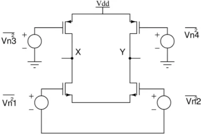
2.2.3 Noise in Differential Pairs
Figure 2.2 shows a differential pair with the overall noise modelled.
8 Theoretical Background We can obtain the input-referred noise voltage by taking into account the output noise of M3 and M4. The drain noise current of M3 is divided between ro3 and the resistance seen looking
into the drain of M1. This resistance RX =ro4+2ro1. Denoting the resulting noise currents
flowing through ro3 and RX by InA and InB, respectively , we have: InA =gm3Vn3(2r(ro4o4+2r+2ro1o1)) and
InB=gm3Vn3(2ro4r+2ro3 o1). The former produces a noise voltage gm3Vn3ro3
(ro4+2ro1)
(2ro4+2ro1) at node X with
respect to ground, whereas the latter flows through M1, M2 and ro4, generating gm3Vn3(2r(ro4o3+2rro4)o1)
at node Y, with respect to ground. Thus, the total differential output noise due to M3 is equal to gm3Vn3(r(ro3o3+rro1o1)) . We can conclude then, that the noise current of M3 is simply multiplied by the
parallel combination of ro1and ro3to produce the differential output voltage.
2.3 Amplifiers
The purpose of this section is to enlighten the reader in the analog electronics design fields, namely amplifiers. The reader can find more information about amplifiers here: [12], [13]. Please refer to appendix 2 for more information about basic transistor configurations.
2.3.1 Fully Differential amplifiers
This section deals with one of the most used input stages, the differential pair. Because of its useful characteristics, it is the dominant choice in today’s high performance analog and mixed signal circuits. So, what makes us choose differential over single ended operation?
• Environmental noise immunity
• Increase in the maximum achievable voltage swings • Simpler biasing
• Higher linearity
Although differential operation brings a lot of benefits, it has a small drawback: the occupied area. This section enlightens the reader on the basic differential pair, a detailed analysis on its mode of operation, and possible negative feedback topologies, as well as common mode feedback topologies.
2.3 Amplifiers 9
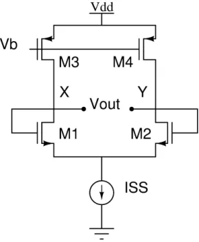
2.3.2 Differential pair with load resistors
Figure 2.3: Basic Differential pair
To allow normal operation, it is imperative to ensure that both M1 and M2 stay in saturation. Their mode of operation can move to the triode region if there is a disturbance in the common mode level, affecting their currents. Thus it is important that the bias currents of the devices have minimal dependence on the input CM level. To do that a current source is used.
If the input voltage swing increases (Vin1−Vin2), the circuit becomes more non-linear, due to
one of the transistors absorbing all of ISS (in the worst case scenario), and the other one absorbs
none, thus one of them goes into cut-off and the other remains in saturation. Therefore its max-imum and minmax-imum voltage output varies from VDD and VDD− RDISS. For Vin1=Vin2the circuit
is in equilibrium. The range of the minimum and maximum common mode voltage can also be obtained: M1 and M2 enter the triode region if Vin,CM>Vout1+Vth=VDD− RDISS/2 +Vth, and
if Vin,CM >Vgs1+Vgs3− Vthwe guarantee that both M1 and M2 remain in saturation. Thus we
set limits for Vin,CM : Vgs1+Vgs3− Vth≤ Vin,CM ≤ min(VDD− RDISS/2 +Vth,VDD). Now that the
common mode voltage is defined, we can define the maximum values for the output voltage: it can go as high as VDD, and as low as approximately Vin,CM−Vth.
10 Theoretical Background
2.3.3 Common-mode Response
Figure 2.4: Basic Differential pair with common mode input
One of the most important attributes of differential amplifiers is their ability to suppress the effect of common mode perturbations. In reality, neither the circuit is fully symmetric, nor does the current source exhibits infinite output impedance. By definition AV,CM=VVin,CMout =−(1/(2g(RDm/2))+RSS).
If the resistor of the current source was of infinite value, AV,CMwould be zero. The finite output
impedance of the tail current source results in some common-mode gain in a symmetric differential pair, as seen from the equation. This conclusion was made assuming the circuit was perfectly symmetrical, but what if it was not? Assuming there is a mismatch in a resistor, RD1=RD1+∆,
what happens to Vout1 and Vout2 as Vin,CM increases? Assuming M1 and M2 are symmetrical we
obtain:∆Vout1=−(1+2g∆VmRin,CMSS)(RgmD1+∆) and∆Vout2=−(1+2g∆Vmin,CMRSSg)(RmD2), thus, a common mode change
at the input introduces a differential component at the output. This is a problem because if the input of the differential pair includes both a differential signal and common mode noise, the circuit corrupts the amplified differential signal by the input CM change. In conclusion, the common mode response of differential pairs depends on the output impedance of the tail current source and the asymmetries in the circuit.
2.3 Amplifiers 11
2.3.4 CMOS Differential Pair
Figure 2.5: Basic Differential pair with CMOS active load
In this case the load is done through an active load (diode connected or current-source load). The small signal gain is: AV =gmN(ron||rop). The diode connected loads consume voltage
head-room, thus creating a trade-off between the output voltage swings, the voltage gain, and the input common mode range. There are a lot of techniques that can be used to improve some of the char-acteristics of this topology. For example, using current-source loads( 2.7) can help reduce the gm
of the diode connected load devices, by aiding in supplying the bias current, thus reducing their currents rather than their aspect ratios, which will help increase the differential gain. However, the small signal gain of the differential pair with current-source loads is relatively low; One way to solve this problem is to increase the NMOS and PMOS output impedance through means of cascoding ( 2.6). This method increases differential gain, but its drawback is an increase in the consumption of more voltage headroom.
12 Theoretical Background
Figure 2.6: Differential pair with cascoding
Figure 2.7: Differential pair with current source load
2.3.4.1 Frequency Response
This section deals with the analysis of the frequency response of the differential pair, both for differential signals and common mode signals.
As we can see in Figure 2.8, its frequency response is similar to that of a common source stage, exhibiting miller multiplication of Cgd. In this case both +Vin2/2and−Vin2/2 are multiplied
by the same transfer function, that brings us to the conclusion that the number of poles in Vout/Vin
is equal to that of each path (rather than the sum of the number of the poles in the two paths). For common-mode signals, the high frequency gain is determined by the capacitance at node P, which consists of Cgd3,Cdb3,Csb1and Csb2. If M1-M3 are wide transistors this capacitance will
2.3 Amplifiers 13 common mode high frequency gain simply by replacing in the formula the drain resistor and the output resistor of M3 with its own value in parallel with the capacitance seen through that node.
AV,CM=−(∆gm (RD||( 1 (CLs)))) ((gm1+gm2)[ro3||((CPs)+1)1
).
This suggests that, if the output pole is much farther from the origin than is the pole at node P, the common mode rejection of the circuit degrades considerably at high frequencies. For dif-ferential pairs with high impedance loads made with active loads, an analysis can be made for differential and common mode signals separately.
Figure 2.8: Differential pair equivalent half circuit
14 Theoretical Background In this case ( 2.9), G is an ac ground, because Cgd3 and Cgd4 conduct equal and opposite
currents to that node. As we have a very high load seen from the output (ro3||ro1), the dominant
pole is given by ((ro3||ro1)CL)(−1). The common mode behaviour of this circuit is similar to the
one analysed before. Let us consider now a differential pair with an active current mirror.
Figure 2.10: Differential pair with mirror pole representation
In contrast to the fully differential configuration, this topology does not have the same transfer function on both sides. The path consisting of M3 and M4 includes a pole at node E, which is known as the mirror pole. This pole is greater in magnitude than the output pole, and it is given by Cgs3,Cgs4,Cdb3,Cdb1 ,and the miller effect of Cgd1and Cgd4. Even if only Cgs3and Cgs4
are considered, the severe trade-off between gm(1/gm3is the impedance seen through that node)
and Cgs of PMOS devices results in a pole that greatly impacts the performance of the circuit.
Through some abbreviations, the poles of this circuit are as follows:ωp1=1/(CL(roN||roP))and
ωp2=gmP/CE where CE is the total capacitance at node E. There can also be obtained a zero in
the left half plane, and its value is 2ωp2. In summary, fully differential circuits do not possess a
mirror pole, another advantage against single ended circuits.
2.3.5 Stability and Frequency Compensation
Stability and frequency compensation is a topic that has to be taken into account by analog cir-cuit designers. If we want to achieve higher output voltage swings, then a two stage operational amplifier is required, and the study of such amplifier’s stability is of great importance.
2.3 Amplifiers 15
Figure 2.11: Two-stage operational amplifier
Observing figure 2.11, we can identify 3 poles, one at A1(A2), another at B1(B2) and another at X(Y ). As stated in the previous section the pole at X lies in the high frequencies. Since the small signal resistance seen at A1 is high, even the capacitances of M3,M5 and M9 can create a pole close to the origin. In the output, the resistance can be small, however, CLcan be high, making the
circuit exhibit two dominant poles. A bode plot of this circuit can be found in [13]. Since the poles at A1 and B1 are relatively close to the origin, the phase approaches −180owell below the third
pole. This implies that the phase margin may be close to zero even before the third pole contributes with its phase shift. So, how do we compensate this circuit? The goal is to move a dominant pole towards the origin so as to place the gain crossover well below the phase crossover. However, the unity gain bandwidth after compensation cannot exceed the frequency of the second pole of the open-loop system. Thus, the magnitude of ωp,A1 must be reduced, however, the available
bandwidth will be limited to approximatelyωp,A1, which is a low value. Furthermore, the small
magnitude of the required dominant pole translates to a very large compensation capacitor, which is not desired. In [13], a better approach is taken, also known as Miller compensation, that creates a large capacitance at node A1, and moves the output pole away from the origin.
2.3.6 Common-mode Feedback
As we have seen in the previous sections, fully differential amplifiers have many advantages in comparison with their single ended counterparts, such as greater output swings, avoiding mirror poles, thus achieving a higher closed loop bandwidth. However, high gain differential circuits require common-mode feedback. For a better understanding of the need of this type of feedback, an example is required. In a differential amplifier, sometimes negative feedback is required, and for that, we short the inputs and the outputs of the circuit. The input and output common mode levels are well defined in this case: VDD− RDISS/2. Now suppose the load resistors are replaced
16 Theoretical Background by PMOS current sources , so as to increase the differential voltage gain. Figure 2.12 represents this example.
Figure 2.12: Differential pair with inputs shorted to outputs
What is the common mode level at the output node? Since each of the input transistors carry half of the tail current, the CM level depends on how close the PMOS current values are to that value. Suppose there is a mismatch in the PMOS and NMOS current mirrors defining an error between their drain currents and ISS/2. If we assume the drain currents of both M3 and M4 in
the saturation region are slightly greater than ISS/2, both M3 and M4 must enter the triode region
so that their drain currents match ISS/2. Conversely, if their drain currents are inferior to ISS/2
then both Vout1 and Vout2 must drop so that M5 enters the triode region, thereby producing only
2ID3,4. The above difficulties arise because in high gain amplifiers, we want to use a p-type current
source to balance an n-type current source. The difference between the currents, IPand INflows
through the intrinsic output impedance of the amplifier, creating an output voltage change equal to (IP− In)(RP||Rn). Since the current error depends on mismatches and the load associated with
it is high, the voltage error can become very large, thus driving the n-type or p-type current source into the triode region. It is emphasized that differential feedback cannot define the CM level. As expected, in high gain amplifiers, the output CM level is quite sensitive to device properties and mismatches and it cannot be stabilized by means of differential feedback. Thus, a common mode feedback network must be added to sense the CM level of the two outputs and accordingly adjust one of the bias currents in the amplifier. CMFB consists of three operations:
2.3 Amplifiers 17 • Comparison with a reference
• Returning the error to the amplifier’s bias network
Recalling that Vout,CM= (Vout1+Vout2)/2, a resistive divider can be employed as shown in figure
2.13.
Figure 2.13: Common-mode feedback with resistive sensing
This generates a voltage Vout,CM=(R1Vout1(R1+R+R22V)out2), that is equal to (Vout1+Vout2)/2 if the
re-sistors are equal. The difficulty here is that both rere-sistors must be much greater than the output impedance of the amplifier so as to avoid lowering the open loop gain. Such large resistors occupy a very large area and suffer from substantial parasitic capacitance to the substrate. To eliminate the resistive loading, we can interpose source followers between each output and its corresponding resistor as seen in figure 2.14.
18 Theoretical Background
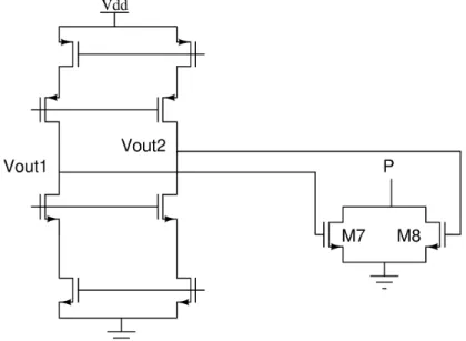
Figure 2.14: Common-mode feedback with source followers
This technique produces a CM level that is in fact lower that the output CM level by the gate-source voltage of transistors M7/M8. It is also important to state that R1and R2or I1and I2must
be large enough to ensure that M7 or M8 can handle a large differential swing on the output. However, this sensing method has an important drawback: it limits the differential output swings (even if the resistors and the currents are large enough) by approximately the threshold voltage. Another type of CM sensing can be seen in figure 2.15:
Figure 2.15: Common-mode feedback with MOSFETs operating in deep triode region
In this type of sensing, we use two transistors in deep triode region, introducing a total impedance that is equal to the parallel of M7 and M8 output resistors, which vary with the width,
2.3 Amplifiers 19 the length of the transistors and Vout1+Vout2. If both the outputs rise together, then the total load
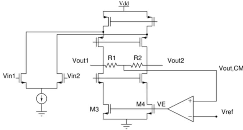
imposed by the transistors will drop, whereas if they change differentially, the load of one transis-tor will increase and the other will decrease. As the resistransis-tor-based sensing method, this method also limits the output voltage swing. Now that we have a method of sensing the CM level, it is imperative to compare it with a reference and return the difference to the bias network. To do this, an op amp can be employed, connected to the NMOS current sources, as we can see in figure 2.16:
Figure 2.16: Sensing and controlling the output CM level
The mode of operation is as follows: if both the output voltages increase, so does VE, thus
increasing the drain currents of M9 and M10 and lowering the output CM level. It can also be interpreted as a form of forcing the CM level of both the outputs to the value of the reference, if the open loop gain is high. This type of feedback can be applied to the PMOS current sources as well. In some cases, the feedback can be used to control only one tail current source, to allow optimization of the settling behaviour. As we have seen, both M9 and M10 were fed by the error coming from the opamp. This technique consists of using only one of them to receive the error, whilst the other is biased at a constant current.
2.3.7 Class Type of Amplifiers
This section provides the reader with an insight about the possible classes of the amplifiers. In our case, it is only pertinent to study the A class , the B class and the AB class. For more information on amplifier class types the reader can find it here : [14].
2.3.7.1 Class A
This is the most linear of the classes, meaning the output signal is a truer representation of the input. Here are the characteristics of the class:
• The output transistor conducts for the entire cycle of the input signal. In other words, they reproduce the entire waveform in its entirety.
20 Theoretical Background • These amplifiers work at higher temperatures, as the transistors in the amplifier are on and
running at full power all the time.
• There are no conditions to turn the transistors on/off. That does not mean that the amplifier is never off or can never be turned off; it means the transistors doing the work inside the amplifier have a constant flow of current through them, also known as bias.
• Class A is the most inefficient of all power amplifier designs, averaging only around 20%. Because of these factors, Class A amplifiers are very inefficient: for every watt of output power, they usually waste at least 4-5 watts as heat. Because of this, they run hotter than the other class types, increasing somewhat the thermal noise of the devices. All this is due to the amplifier constantly operating at full power. The upside is that these amplifiers are the most enjoyed of all amplifiers. Since the transistor reproduces the entire waveform without ever cutting off, the waveform is more linear; that is, it contains much lower levels of distortion.
2.3.7.2 Class B
In this amp, the positive and negative halves of the signal are dealt with by different parts of the circuit. The output devices continually switch on and off. Class B operation has the following characteristics:
• The input signal has to be a lot larger in order to drive the transistor appropriately. • This is almost the opposite of Class A operation.
• There has to be at least two output devices with this type of amplifier. The output stage employs two output devices so that each side amplifies each half of the waveform. Either both output devices are never allowed to be on at the same time, or the bias for each device is set so that the current flowing in one output device is zero when not presented with an input signal.
• Each output device is on for exactly one half of a complete signal cycle.
These amps run cooler than Class A amps, but the linearity is not as pure, as there is a lot of "crossover" distortion, as one output device turns off and the other turns on over each signal cycle. This type of amplifier design, or topology, gives us the term "push-pull," as this describes the tandem of output devices that deliver the signal to your speakers: one device pushes the signal, the other pulls the signal.
As mentioned before, the input signal has to be a lot larger, meaning that from the amplifier input, it needs to be "stepped up" in a gain stage, so that the signal will allow the output transistors to operate more efficiently within their designed specifications. This means more circuitry in the path of your signal, degrading the signal even before it gets to the output stage. The efficiency of such topology wanders around the 60 per cent, and its linearity is inferior to that of class A, as there is a trade-off between efficiency and linearity.
2.3 Amplifiers 21 2.3.7.3 Class AB
This is the compromise between both classes, A and B. Class AB operation has some of the best advantages of both Class A and Class B built-in. Its main benefits are linearity comparable to that of Class A and efficiency similar to that of Class B. Most modern amp designs employ this topology.
Its main characteristics are:
• In fact, many Class AB amps operate in Class A at lower output levels, again giving the best of both worlds
• The output bias is set so that current flows in a specific output device for more than a half the signal cycle but less than the entire cycle.
• There is enough current flowing through each device to keep it operating so they respond instantly to input voltage demands.
• In the push-pull output stage, there is some overlap as each output device assists the other during the short transition, or crossover period from the positive to the negative half of the signal.
There are many implementations of the Class AB design. A benefit is that the inherent non-linearity of Class B designs is almost totally eliminated, while avoiding the heat-generating and wasteful inefficiencies of the Class A design. And as stated before, at some output levels, Class AB amps operate in Class A. It is this combination of good efficiency (around 50) with excellent linearity that makes class AB the most popular amplifier design.
2.3.8 Instrumentation Amplifiers
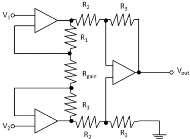
Probably the most popular among all of the specialty amplifiers is the instrumentation amplifier (in-amp). The in-amp is widely used in many industrial and measurement applications where dc precision and gain accuracy must be maintained within a noisy environment, and where large common-mode signals (usually at the ac power line frequency) are present. It may come to mind that an amp might be the same as an op-amp , but several differences exist between them. An in-amp is a precision closed-loop gain block. Normally, it has a pair of differential input terminals, and a single-ended output that works with respect to a reference. Usually the feedback is done internally, and there is a gain setting resistor. Its input impedance is quite high, and its CMRR usually surpasses the 80 dB mark. The typical instrumentation amplifier topology can be found in figure 2.17.
22 Theoretical Background
Figure 2.17: Typical Instrumentation Amplifier
Typical expected characteristics of a in-amp are: low noise, low offset, high gain , high input impedance and high CMRR. In the standard topology those are obtained by its three op amp configuration. The gain in this case is defined by Rgain.
Chapter 3
Bibliographic Review
This chapter has the intent to provide the reader with the technological trends on instrumenta-tion amplifiers until 2013. An explanatory and critical approach is taken when addressing every relevant article.
3.1 Gm variation in rail-to-rail input stage
A rail-to-rail input stage is usually built from two differential pairs, a PMOS and a NMOS. This is due to the fact that to achieve rail-to-rail operation, we must ensure operation over the entire input common-mode voltage. The NMOS deals with the most positive voltage values in the input, whilst the PMOS deal with the most negative. However, in the middle region both pairs are active, bringing us to the conclusion that the rail-to-rail technique entails a problem. In the middle of the rail, both transistor types are active, making the total gm twice as big than it usually is in the voltage extremes. This situation can be better understood by observing figure 3.1.
Figure 3.1: Gm variation along the supply rail.
With a varying input gm, stability problems arise as the unity gain frequency of the amplifier depends on the input gm. This derives from the fact that altering the input gm may alter pole locations and, therefore, may affect the phase margin, which is undesired. There are a lot of
24 Bibliographic Review techniques that deal with this problem. As the reader may have noticed, without a constant gm technique the variation is 100 per cent, as the total gm in the middle area equals twice the normal gm in the extremes.
In this section, some of the most relevant techniques are presented.
3.1.1 Dc shifting circuit to obtain overlapped transition regions
This gmcontrol technique is based upon the overlapping of the gmof both input transistors (NMOS
and PMOS), and it was originally presented in [2]. The idea behind this is to shift the input voltage to one of the input pairs (either the NMOS or the PMOS), so that one curve is shifted towards the other, until they overlap, as seen in figure 3.2.
Figure 3.2: Gmn vs Gmp along the supply rail. Figure obtained from [9]
In this case the total transconductance will be nearly constant. The level shifter can easily be implemented by a common-source voltage-follower, which is controlled by the current that passes it (Ibcontrols Vgs. The circuit with the level-shifters can be seen in figure 3.3.
3.1 Gm variation in rail-to-rail input stage 25 In this image, M5 and M6 are the level shifting transistors, and the voltage shifted can be controlled by Ib.
Working Principle
The input voltages are shifted by M5 and M6 by |Vgs5,6| towards the positive supply rail, so
the transition region for gmpis shifted by the same value towards the negative supply rail. The
transition regions of gmnand gmpoverlap and we can obtain a constant gmover the common-mode
range. A very small variation can be obtained if the dc shift level is well tuned.
3.1.2 Current Summing Technique
The technique presented focus on summing the square root of the p current and the n current, using a square root circuit. This technique was originally presented in [3] For a balanced input pair it can be proved that gmt=gmn+gmp=√2K(√In +√Ip), so in order to keep gm constant we just
have to keep the sum of the currents constant. This circuit can be seen in figure 3.4.
Figure 3.4: Current Summing Circuit
• Vsg11+Vsg10=Vsg8+Vsg9=constant;
• I f (W /L)8= (W /L)9thenp(ID8) +p(ID9) =constant;
• The input transistors work in strong inversion region;
• The square root circuit M7-M11 keeps the sum of the square-roots of the tail currents of the input pairs and then the gm constant;
• The current switch , M5, compares the common-mode input voltage with Vb and decides
26 Bibliographic Review At the extreme voltages, either the p pair or the n pair receive Ib=4Ire f. If the current through
M7 is larger than 4Ire f the current limiter M6 limits the current of M7 to 4Ire f =Iband directs it
to the P input pair.
The circuit is somewhat complex and the functionality relies on the square law of MOS tran-sistors. For current sub-micron processes, this law is not closely followed, which may introduce a larger error in the total transconductance.
3.1.3 Gm Control Through the Use of an Electronic Zener
This technique relies on the use of an electronic zener to keep Vgsn+Vsgp constant, and it was
originally presented in [4]. The formula for the total gm in the input pair is as follows: Gmt=
gm1+gm2=2K(Vgsn+|Vgsp|˘Vtn− |Vtnp|, thus making Gmt constant means keeping Vgsn+|Vgsp|
constant. As the reader can see in figure 3.5, the floating voltage source keeps that sum constant, and its value is Vf s=gmt/2K +Vtn+|Vt p|.
Figure 3.5: Input stage with a Voltage source
One way to implement this voltage source is by using diode connected MOSFETs as seen in figure 3.6.
3.2 Instrumentation Amplifiers Topologies 27 However, this circuit cannot achieve the same performance as with an ideal voltage source. Figure 3.7 presents a more precise implementation of the voltage source.
Figure 3.7: A more precise implementation of the electronic zener
In this topology, the electronic zener is implemented by transistors M5-M8. M5 and M7 are current mirrors, Id5=Id7, thus making the current through M5 and M6 constant. This configuration is equivalent to a zener with very low resistance.
3.1.4 Comparative Analysis
From all the topologies here presented, the one who presents the best gm variation, is the one with overlapped transition, presenting only a ± 4 per cent variation. Its only limitation is that it’s sensitive to Vt and power supply voltage change, but in this case , that is not a problem, making
this topology an obvious choice.
3.2 Instrumentation Amplifiers Topologies
This section focus on the suitable topologies that can be used to develop instrumentation ampli-fiers.
3.2.1 The Fully Balanced Differential Difference Amplifier (FBDDA)
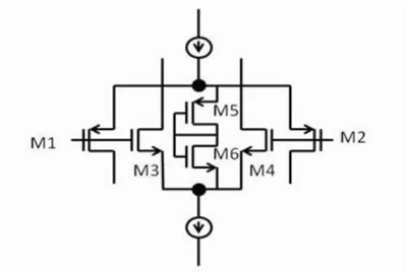
The FBDDA topology is a recent one, with distinctive characteristics. Unlike common FDDA’s, FBDDA’s employ 4 inputs, as one can see in image 3.8.
28 Bibliographic Review
Figure 3.8: The Fully Balanced Differential Difference Amplifier
The reader might easily come to the conclusion that this topology entails more area, but it allows for more dynamic range and a higher input impedance value, as well as the ordinary advan-tages achieved by the differential pairs. This configuration finds its applications in a wide range of areas. In a similar way to the much known op amp configuration, the FBDDA also allows for inverting or non inverting configurations as well as buffer operation. Image 3.9 presents the fundamental applications for the FBDDA.
3.2 Instrumentation Amplifiers Topologies 29
Figure 3.9: Several applications of the FBDDA. (a) single ended buffer. (b) Fully differential buffer. (c) Single ended noninverting amplifier. (d) Fully differential noninverting amplifier. (e) Single ended state-filter. (f) Fully differential state-variable filter. Image obtained from [5]
It is also imperative to know the possible negative feedback combinations. Image 3.10 presents all of the possible combinations. These different topologies present different charac-teristics as well.
30 Bibliographic Review
(a)
(b)
Figure 3.10: Negative Feedback combinations (a) and (b). Outputs are fed back to the same differential pair (a). (b) outputs are fed back to different differential pairs.
In [5] it was presented the original FBDDA topology with a cmfb circuit, as well as a class AB output stage. Good results were achieved. Information about FDDAs is not presented here because the FBBDA is , so to speak, an upgrade to that topology and more suitable for instrumentation amplifiers development. However, if required, more information on FDDAs can be found here: [15], [16], [17], [18] and [19].
3.2.2 Pseudo-Differential Amplifiers (PDA)
PDAs are a variation of FDDAs. The major difference is that they do not use a current source in the input pair, as seen in figure 3.11. This allows for higher swings, as the current source does not limit the source voltage of the input transistors. However, this topology suffers in terms of common-mode response, as its CMRR is close to 0 dB , since the differential gain equals the common-mode gain.
3.2 Instrumentation Amplifiers Topologies 31
Figure 3.11: Pseudo-Differential Amplifier.
[6] presents a novel PDA topology with a rail-to-rail CMFB detector using a transconductance and a transimpedance amplifier. Low power consumption and small area is achieved.
3.2.3 Chopper-Stabilized Amplifiers
Chopper-stabilized amplifiers are amplifiers that present low noise. They are mainly composed by a pre-modulation block, followed by an amplifier, and ending with a demodulator. This allows to amplify the signals in a desired frequency, reducing flicker noise immensely and achieving very low offset. However, chopper amplifiers usually require switching capacity and occupy a rather large area.
In [7] a novel chopper amplifier topology is presented , that combines the chopper topology with the DDA topology. This allows for a very low noise and a low offset amplifier. It is a fairly good topology, however, in terms of area, it is quite big.
3.2.4 Comparative Analysis
When facing the 3 possibilities to implement an inamp, one should consider the goals he has in mind for the amplifier. The chopper amplifier is better in terms of noise and offset, however in terms of area it would be quite large, and it would imply the use of switching, complicating the circuit. While the PDA presents good characteristics, it lacks the overall better characteristics that the simple DDA presents, namely the much required high CMRR. Since the goal of this thesis was to make a dedicated inamp and at the same time maintain good characteristics to be used in other
32 Bibliographic Review kind of applications, the DDA topology was the one that stood out. Another reason for the choice of this topology was the fact that there are not any instrumentation amplifers based on the FBDDA topology yet.
Chapter 4
Development of the Instrumentation
Amplifier
The first step to take in developing an amplifier is to acknowledge the environment in which it will work, and the signals it will amplify. In this case, the environment is standard (normal temperature, pressure and humidity values), and it will reside on a chip to be placed near the electrodes. This first condition rapidly leads us to the conclusion that the power consumption of the chip has to be very low, to increase the battery life, and its area has to be small, to avoid provoking discomfort on the patient. Regarding the signals, we already know that they are low frequency, and low voltage implying high precision and low noise. These are the top requirements to be satisfied, things such as bandwidth and slew rate, for example, are not so important in the design of such amplifier. Besides these characteristics, there are the usual op amp characteristics that have to be fulfilled, such as the Phase Margin, gain, and others. For a better visualization of the global requirements, the reader can find in table 4.1 an organized view of the desired characteristics.
With the requirements in mind, the beginning of the development of the topology is quite simple. The differential pair is a fairly good start, as explained in the previous chapters, and so, the adopted topology was as follows.
The block diagram of the proposed amplifier can be seen in figure 4.1. The two differential transconductance amplifiers are the input differential pairs. The currents from the complementary inputs sum, following to a gain amplifier (gain and output stage). This type of configuration is advantageous because it entails high input impedance and increased dynamic range due to the use of not one, but two differential pairs. This is a recent topology, and there are no instrumentation amplifiers implemented yet with it. With the advantageous characteristics, its high flexibility and the fact that it was a recent topology it was set in stone that the amplifier would be built based on this topology.
34 Development of the Instrumentation Amplifier Table 4.1: Requirements for the amplifier, regarding myoelectric signals.
Characteristic Minimum Required Goal Optimum Value Bandwidth 10*500 Hz = 5000 Hz >5000 Hz
PSRR 80dB >80dB
CMRR 80dB >100dB
Offset 100u <100u
Integrated Noise (10Hz - 300Hz) 2µV2 <2µV2
Input Impedance 1M >1M
Open Loop Gain 80dB >80dB
Input Swing Arbitrary rail-to-rail Output Swing Arbitrary rail-to-rail
Output Impedance 5K 500
Phase Margin 60o >70o
Gain Margin <0 -30
Slew Rate Arbitrary >1 V/us
Figure 4.1: Block diagram of the instrumentation amplifier - FBDDA topology.
4.1 Input Stage
The input stage is a derivation from the initial topology - it has 2 NMOS differential pairs as well as 2 PMOS differential pairs that entail rail-to-rail operation. This is due to the fact that when the input voltage is near the positive rail, the NMOS are active, while on the other hand, if the input voltage is close to the negative rail, the PMOS are active. In either case, the complementary pairs are cut-off. To maintain the circuit balanced, the NMOS and the PMOS currents are summed up, through a current mirror , allowing for the correct functioning of the circuit upon mid rail operation (both pairs are active). However, this entails a problem, the equivalent gm of the input pair is not constant, affecting the circuit stability and gain.
Transistors M1-M8 are the differential pairs, both NMOS and PMOS. Transistors M9-M12 are the gm-control transistors. These transistors are responsible for performing a DC shift in the input voltage, thus making the transistors operating-zones overlap, as explained in the bibliographic
4.1 Input Stage 35 review, allowing for a constant gm throughout the input voltage range. Transistors M13-M20 are current sources that supply the differential pairs, as well as the dc shifting transistors. Since we have NMOS and PMOS differential pairs, we need to have a way to sum the currents in both pairs. Transistors M21-M24 take care of that problem, as they mirror the current from the PMOS branch, to the NMOS. In the end, both currents are summed and carried out to the gain stage (Out1 /Out2). As for the load of the NMOS differential pairs, a crosscoupled load was used -transistors M25-M28. This allows for a higher CMRR, since the impedance they offer is higher for differential signals, and smaller for common-mode signals, unlike the simple PMOS load. Figure 4.2 presents both types of load.
(a) Differential pair with a PMOS active load.
(b) Cross-coupled load on a single differential pair.
Figure 4.2: Types of load. (a) simple PMOS active load. (b) cross-coupled load
Even though, the PMOS active load has to offer a slightly higher output impedance, the cross coupled load offers other types of advantages. For common-mode signals, the impedance it
of-36 Development of the Instrumentation Amplifier Table 4.2: Transistor sizes for the input stage.
Transistor Size (W/L) M1-M4-M5-M8 50.1/5 M2-M3-M6-M7 150/5 M13-M14-M21-M22-M23-M24 10/1 M16-M19 30/1 M15-M17-M18-M20 25/1 M25-M26-M27-M28 15/1
fers is quite low, approximately 1/gm, and for common-mode signals, it is approximately Ro3/2
assuming the transistors have the same size, since the total impedance seen from the drain is the parallel of (1/gm3//− 1/gm4)with Ro3//Ro4. This increases the CMRR, as well as permits the
CMFB circuit to drive the current source in the gain stage instead of the current source in the input stage. This would complicate the CMFB circuit, as we would need to have two outputs, instead of one: one for the NMOS current sources, and another for the PMOS. The cross-coupled load is clearly advantageous. With this being said, the reader can find the total input stage in figure 4.3.
Figure 4.3: Input Stage of the Instrumentation Amplifier The sizes of the transistors can be found in table 4.2:
4.2 Gain stage and Output Stage
As for the gain stage, a simple common-source was used, with miller compensation. The diode connected NMOS function is to balance the gain branch and the branch composed by transistors M29-M31 in terms of voltage. Compensation was made through a Poly capacitor and a triode
4.2 Gain stage and Output Stage 37 transistor. This triode transistor had its bias point controlled by two other diode connected de-vices, but because of the total power consumption, they had to be removed, making the control of resistance of the transistor externally.
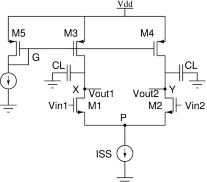
This output stage is based on the one developed by Phillip Allen, in [10]. It achieves rail-to-rail operation, as well as a low output resistance. This topology in particular also guarantees offset protection. Rail-to-rail operation is achieved through the use of transistors in Common-Source configuration. However, the reader might wonder how is the low output resistance achieved, if we are to use Common-Source transistors. This is due to a feedback network applied directly on the output, thus reducing the output resistance by a factor of (1+Loop Gain). In this case, the loop gain is determined by the error amplifiers, as seen in figure 4.4
Figure 4.4: Negative Feedback applied on the output
In this case, the error amplifiers are simple differential pairs. Transistors M1 - M8 constitute the differential pairs.Transistors M35 and M34 are the output transistors, and their current is stabi-lized in case of an offset in the error amplifiers by the feedback loop composed by M29-M33 and M14. Figure 4.5 portrays this situation.
38 Development of the Instrumentation Amplifier If an offset occurs between the error amplifiers, the current that flows through the output drivers is uncontrolled, since the current that flows through them is controlled by the current mirrors in the differential pairs. The feedback loop that controls this works as follows. If an offset exists, the output voltage in the error amplifier A1 increases, causing the current in M6 and M9 to decrease. This decrease in the current is mirrored in transistor M8A, which will represent a decrease in its gate-source voltage. This decrease in its Vgswill balance out the increase in the offset voltage in
the error loop, consisting of Vos, M8 and M8A. In this manner, the currents in the output drivers, M6 and M6A , are balanced. Figure 4.6 presents both the gain stage, and the complete output stage.
Figure 4.6: Gain and Output Stage
Because M35 can supply large amounts of current, we must ensure that this transistor is off during the negative half-cycle of the output voltage swing. For large negative swings, the drain of transistor M16 pulls to Vss, turning off the current that biases its respective error amplifier. The gate of M35 is then floating and tends to pull towards Vss, turning this transistor on. This topology already deals with this situation, keeping M35 off for the large negative swings, due to transistors M9-M12. This swing protection circuit will degrade the step response of the amplifier, because the unity-gain amplifier not in operation is completely turned off. As M35 turns off, M9 and M10 pull the drains of transistors M3 and M4 , respectively. As a result, transistor M6 is turned off, and any floating nodes are eliminated. Transistors M11 and M12 deal with its positive counterpart, in the same manner.
Short-circuit protection is also included in the design of the amplifier [10]. Transistors M19-M28 compose the short circuit protection circuit, and its operation goes as follows. M23 senses the output current through transistor M35 and in the event of large output currents, the biased inverter formed by M20 and M24 trips, thus enabling transistor M28. Once it is enabled, the gate of M35 is pulled towards the positive rail, making its current limited to a maximum value, dependant on its size. In a similar manner, M24-M28 deal with the NMOS output driver. Regarding the rest of
4.3 CMFB 39 Table 4.3: Transistor sizes for the gain and output stage.
Transistor(s) Size (W/L) M1,M2,M7,M8,M16,M31 5/1 M3,M4,M5,M6,M17 15/1 M34 7/0.35 M35 21/0.35 M9,M10,M19,M24,M30 3/1 M11,M12,M29 1/1 M15 10/1 M23 2.5/1 M28 7/4 M20 7.5/1 M22 30/1 M33 80/1 M18 8/1 M21 40/1 M26,M27 1.5/1 M25 2/1 M14 42/1 Cc 10p Cco 11p
the transistors, M13 is the gain transistor, and the rest of the transistors are current-sources, with the exception of M36-M38. These are the triode transistors, biased by an external voltage.
Table 4.3 presents the sizes of the transistors that compose the gain and the output stage.
4.3 CMFB
The CMFB topology development was quite hard to develop. Rail-to-rail MOS CMFB detec-tors were mandatory, since resisdetec-tors and capacidetec-tors occupied a large area. In the beginning, a simple differential common-mode detector was implemented, along with an error amplifier. This common-mode detector initially had two input differential pairs, one NMOS and one PMOS, as well as two outputs, one for the PMOS current mirrors and another for the NMOS current mirrors because at the time the CMFB was feeding the input stage, instead of the gain stage. But after the insertion of the cross-coupled load, there was no longer need for two outputs. However, still no rail-to-rail results were being achieved. This was due to the current sources that fed the input pairs, that did not allow the source voltage of the input transistors to go to zero. This affected the rail, and the answer for this was later found in [11]. The use of pseudo-differential pairs, allows for a higher swing, since there is no current source for the input transistors. There were other ways to implement a rail-to-rail CMFB, but they were simple ideas at the time . One of these possibilities, consisted in implementing a charge-pump to increase Vdd solely on the CMFB input stage. That would allow rail-to-rail operation. An initial topology was implemented, but good results were
40 Development of the Instrumentation Amplifier not achieved, and so the decision was made about the CMFB - The topology in [11] was used. Its topology can be seen in figure 4.7.
Figure 4.7: The Common-mode Feedback Detector. Image obtained from: [11]
This is solely the common-mode detector. Afterwards an error amplifier is applied, consisting in a simple differential pair with PMOS load, as seen in image 4.8.
Figure 4.8: The Error Amplifier for the CMFB Circuit. The transistor sizes for the CMFB detector are present in table 4.4.
4.3 CMFB 41 Table 4.4: Transistor sizes for the cmfb detector.
Transistor(s) Size (W/L) M1A - M2A - M7A - M3B -M4B 5/4 M3A - M4A - M1B - M2B - M7B 15/4
M5A - M6A 15/8
M5B - M6B 5/8
As for the error amplifier, the reader can consult the transistor sizes used in table 4.5 . This topology need not be the gain amplifier of the global circuit - it can work as a pre-amplifier followed by a PGA.
Please refer to appendix 1 for expressions for the amplifier.
Table 4.5: Transistor sizes for the error amplifier. Transistor(s) Size (W/L)
M1 - M2 5/2 M3 - M4 15/2 M5 (Iss) 15/1
Chapter 5
Simulation and Results
Many simulations were performed, as one should in the case of an amplifier. This chapter con-tains all the simulations made to the amplifier, as well as the layout produced and the simulations performed on the layout. Please refer to appendix 1 for information on the simulations done.
5.1 Characterization of the amplifier
The simulation that follows is in regard to the amplifier connected in the non-inverting configura-tion, withβ = 0.1 for simulation purposes, as seen in image 5.1.
Figure 5.1: Non-Inverting configuration of the amplifier
The stimuli applied to the amplifier was as follows: • Supply Voltage : V ss = −1.65;V dd = 1.65
• Bias: V bn = −725.2mV ;V bp = 557.4mV ;V re f = 0;V btn = 1.126V ;V bt p = −877.2mV • Output : Rload = 10k,Cload = 10p
• Input : V (dc) = 0,Vpp=2mV, f requency = 1K
One can find the amplifier’s frequency response in image 5.2. 43


![Figure 3.3: Rail-to-rail input stage with dc shift gm control. Figure obtained from [9]](https://thumb-eu.123doks.com/thumbv2/123dok_br/19175949.943189/44.918.263.601.821.1000/figure-rail-input-stage-shift-control-figure-obtained.webp)