Halyna Korol
Licenciada em Engenharia Electrotécnica e de Computadores
Switching Mode Power Amplifier for Bluetooth
Applications
Dissertação para obtenção do Grau de
Mestre em Engenharia Electrotécnica e de Computadores
Orientador: Luís Augusto Bica Gomes de Oliveira,
Professor Doutor, Universidade Nova de Lisboa
Júri:
Switching Mode Power Amplifier for Bluetooth Applications
Copyright cHalyna Korol, Faculdade de Ciências e Tecnologia, Universidade
Nova de Lisboa
A
CKNOWLEDGEMENTS
Chegando a esta fase, é de reflectir nas inúmeras oportunidades e concretizações, tanto a nível pessoal como a nível profissional, que aconteceram graças à FCT-UNL. Esta, não só é uma instituição com espaço de admirar, mas que também oferece distintas áreas de aprendizagem com professores notáveis nas respectivas áreas. A isto devo um muito obrigado!
Em segundo lugar, gostaria de agradecer a todos os professores do departa-mento de electrónica. Mas devo um especial agradecideparta-mento à professora Helena Fino, porque foi ela que desde princípio criou a minha paixão pela electrónica; ao professor João Goes por ter feito crescer a minha paixão ainda mais, mas desta vez pela micro-electrónica; ao professor Luís Oliveira, que tanto como professor como meu orientador sempre me guiou e sempre me motivou; aos professores João Oliveira, Nuno Paulino e Rui Tavares por serem esplêndidos professores. Um especial obrigado também ao professor Luís Bernardo, André Mora e Anabela Pronto, por serem mais do que professores.
Quero também expressar a minha gratidão para com os meus colegas da sala 3.5, que sem a companhia deles o trabalho nunca seria o mesmo, nem os almoços, nem os pequenos intervalos num espaço que muito bem podia ser chamado de “a nossa casa”. Por isso, a eles, sem exclusão alguma, mesmo os que já “partiram”, outro muito obrigado.
Um obrigado também às pessoas que mais me marcaram neste percurso académico: Jorge Silva, Denise Solange, Dilcarina Duarte, Tiago Bento, Celso Almeida e a Ana Carreira, a minha companheira de comboio.
A
BSTRACT
Modern fully integrated transceivers architectures, require circuits with low area, low cost, low power, and high efficiency. A key block in modern transceivers is the power amplifier, which is deeply studied in this thesis.
First, we study the implementation of a classical Class-A amplifier, describing the basic operation of an RF power amplifier, and analysing the influence of the real models of the reactive components in its operation.
Secondly, the Class-E amplifier is deeply studied. The different types of im-plementations are reviewed and theoretical equations are derived and compared with simulations. There were selected four modes of operation for the Class-E amplifier, in order to perform the implementation of the output stage, and the sub-sequent comparison of results. This led to the selection of the mode with the best trade-off between efficiency and harmonics distortion, lower power consumption and higher output power. The optimal choice was a parallel circuit containing an inductor with a finite value. To complete the implementation of the PA in switch-ing mode, a driver was implemented. The final block (output stage together with the driver) got 20 % total efficiency (PAE) transmitting 8 dBm output power to a 50Ωload with a total harmonic distortion (THD) of 3 % and a total consumption
of 28 mW.
All implementations are designed using standard 130 nm CMOS technology. The operating frequency is 2.4 GHz and it was considered an 1.2 V DC power supply. The proposed circuit is intended to be used in a Bluetooth transmitter, however, it has a wider range of applications.
R
ESUMO
As arquiteturas modernas de transcievers totalmente integradas, requerem
circuitos de reduzida área, de baixo custo, mínimo consumo de energia e alta
eficiência. Um bloco chave emtranscieversmodernos é profundamente estudado
nesta tese, o amplificador de potência (AP).
Em primeiro lugar, estudou-se a implementação de um amplificador clássico Classe-A, descrevendo o funcionamento básico de um amplificador de potência de RF, e analisando a influência dos modelos reais dos condensadores e das bobinas no seu funcionamento.
Em segundo lugar, o amplificador de Classe-E é profundamente estudado. Os diferentes tipos de implementações são revistos e as equações teóricas são derivadas e comparados com as simulações. Foram selecionados quatro modos de funcionamento para o amplificador de Classe-E, a fim de realizar a implementação do andar de saída e a posterior comparação de resultados. Esta comparação levou à seleção do modo com o melhor compromisso entre eficiência e distorção harmónica, menor consumo de energia e potência de saída superior. O escolhido, acabou por ser um circuito em paralelo contendo um indutor com um valor finito. Para completar a implementação do AP no modo de comutação, foi implementado umdriver. O bloco final (andar de saída, juntamente com o driver) tem 20 % de eficiência total (PAE), transmitindo 8 dBm de potência a uma carga de saída de 50
Ω, uma distorção harmónica total (DHT) de 3 % e um consumo total de 28 mW.
Todas as implementações foram projetados usando uma tecnologia CMOS standard de 130 nm. A frequência de trabalho é de 2,4 GHz e foi utilizada uma fonte de alimentação DC 1,2 V. O circuito proposto destina-se a ser utilizado num transmissor Bluetooth, no entanto, tem uma ampla gama de aplicações.
C
ONTENTS
List of Figures xvii
List of Tables xxi
1 Introduction 1
1.1 Background and Motivation . . . 1
1.2 Bluetooth Features . . . 2
1.3 Thesis Outline . . . 3
1.4 Main Contributions . . . 4
2 Power Amplifier Basic Concepts 5 2.1 Efficiency . . . 5
2.2 Output Power . . . 6
2.3 Linearity and Distortion . . . 7
2.4 Transmitter . . . 10
2.4.1 Heterodyne Upconversion . . . 11
2.4.2 Direct Upconversion . . . 12
3 Power Amplifiers 13 3.1 Conventional Amplifiers . . . 13
3.1.1 Class-A . . . 14
3.1.2 Class-B . . . 17
3.1.3 Class-AB . . . 19
3.1.4 Class-C . . . 20
3.2 Switching Amplifiers . . . 21
3.2.1 Class-D . . . 22
3.2.2 Class-E . . . 23
3.2.3 Class-F . . . 24
3.3 Current Source Versus Switched-Mode Operation . . . 26
4 Class-A Power Amplifier 29
4.1 Implementation of the Class-A Power Amplifier . . . 29
4.1.1 Design of Class-A Power Amplifier . . . 29
4.2 Simulations Results . . . 33
4.2.1 Class-A Simulation . . . 34
4.2.2 Class-A Simulation with Real Models of the Reactive Com-ponents . . . 37
5 Class-E Power Amplifier 41 5.1 Class-E Theory . . . 41
5.1.1 Assumptions . . . 44
5.1.2 Circuit Description . . . 45
5.2 Implementation . . . 48
5.2.1 Design of the Output Stage Class-E Amplifier . . . 50
5.2.2 Design of Driver Stage Class-A Amplifier . . . 54
5.3 Simulation Results . . . 57
5.3.1 Output Stage Simulation Results . . . 57
5.3.2 Driver Stage Simulation Results . . . 63
5.3.3 Simulation Results of the Complete PA . . . 65
6 Conclusions and Future Work 71 6.1 Conclusions . . . 71
6.2 Future Work . . . 72
Bibliography 75 A Schematics 81 A.1 Class-A Schematic . . . 81
A.2 RF PA Final Solution Schematics . . . 83
A.2.1 Class-E Schematic . . . 83
A.2.2 Driver Schematic . . . 84
A.2.3 Final Blocks Schematic . . . 85
A.3 Input and Output Ports Setting . . . 85
B CMOS Transistors 87 B.1 Structure of MOS transistors . . . 87
B.2 Basic operation of MOS transistors . . . 89
CONTENTS
C.1 Class-E Cascode Common-Gate Topology . . . 97
L
IST OF
F
IGURES
2.1 Representation of a PA block with the associated powers. . . 7
2.2 1 dB compression point and 3rd order intermodulation intercept (IP3). 8 2.3 Spectrum of the output voltage with harmonics effect. . . 9
2.4 Spectrum of the output voltage with the respective intermodulation products. . . 9
2.5 Simplified block diagram of the transmitter (top) and receiver (bottom) for wireless communication. . . 10
2.6 Block diagram of the Heterodyne transmitter. . . 11
2.7 Block diagram of the Heterodyne transmitter. . . 12
3.1 Classical RF PA with inductive load . . . 14
3.2 Class A stage . . . 16
3.3 Class-A ideal drain voltage and current waveforms . . . 17
3.4 Class-B ideal drain voltage and current waveforms . . . 18
3.5 Class-AB ideal drain voltage and current waveforms . . . 19
3.6 Class-C ideal drain voltage and current waveforms . . . 20
3.7 Drain efficiency and power capability in function of conduction angle . 21 3.8 The Class-D power amplifiers: (a) voltage-mode Class-D (VMCD), (b) current-mode Class-D (CMCD) and their respective currents and voltages 23 3.9 Basic topology of the ZVS Class-E power amplifier. . . 24
3.10 Basic topology of the Class-F power amplifier. . . 25
3.11 The Class-F drain current and drain-to-source voltage: (a) square volt-age, (b) square current. . . 26
3.12 Characteristic curves of drain current versus drain-to-source voltage. . 27
4.1 Basic Class-A PA with circuit biasing and output matching . . . 30
4.2 Small signal circuit of the classic PA. . . 32
4.3 LC matching network . . . 32
4.4 Small signal gain,(S22), and output return losses,(S21). . . 34
4.6 1 dB compression point measured at 2.4 GHz. . . 35
4.7 PAE vs. input power at 2.4 GHz. . . 35
4.8 IP3 vs. input power at 2.4 GHz. . . 36
4.9 Transient results of the drain current and drain-to-source voltage. . . . 36
4.10 Gain (S21) versus frequency . . . 37
4.11 Output return losses (S22) versus frequency . . . 38
4.12 Comparison of the PAE with ideal and real components versus frequency. 38 5.1 Current and voltage waveforms through the switch. . . 42
5.2 Class-E equivalent circuits. (a) ZVS circuit. (b) ZCS circuit. . . 43
5.3 Circuit of single-ended Class-E power amplifier with general load network. . . 44
5.4 TheKP,KL,KC andKXparameters in function ofqfor Class-E design with finite-DC feed inductance. . . 49
5.5 General RF switching power amplifiers blocks. . . 49
5.6 Class-E RF power amplifier. . . 50
5.7 Class-A driver circuit. . . 55
5.8 LC output matching circuits: (a) series inductance, parallel capacitance and (b) series capacitance, parallel inductance. . . 58
5.9 S22 parameter simulation results versus frequency.1 . . . 59
5.10 Transient waveforms of the drain current.2 . . . 60
5.11 Transient waveforms of drain-to-source voltage.2 . . . 60
5.12 PAE simulation versus input power.2 . . . 61
5.13 total harmonic distortion (THD) simulation versus input power.2 . . . 61
5.14 Output power simulation versus input power.2 . . . 62
5.15 Results of the Driver: a) output power; b) voltage gain. . . 64
5.16 PAE and THD of the driver. stage. . . 64
5.17 Transient waveforms of the Driver: a) drain current (top) and drain-to-source voltage (bottom); b) output voltage (top) and input voltage (bottom). . . 65
5.18 Simulation results of the two designs versus input power.2 . . . 66
5.19 Output power simulation of the two designs versus input power.3 . . . 66
5.20 Transient Response of the drain current and drain-to-source voltage. . 68
5.21 Transient Response of the input voltage, output voltage and voltage from the driver. . . 68
LIST OFFIGURES
A.2 Schematic of the Class-A power amplifier with real models of the LC
components. . . 82
A.3 Schematic of the Class-E power amplifier with parallel-circuit operation mode. . . 83
A.4 Schematic of the simulated driver block. . . 83
A.5 Schematic of the Class-A driver. . . 84
A.6 Schematic of the simulated driver block. . . 84
A.7 Schematic of the blocks, one containing driver schematic and other output stage schematic. . . 85
A.8 Definition of the input and output ports parameters. . . 85
B.1 Basic geometric top view of a CMOS transistor. . . 87
B.2 An internal structure of an NMOS transistor. . . 88
B.3 An internal structure of an PMOS transistor. . . 88
B.4 Commonly used symbols for NMOS and PMOS transistors. . . 89
B.5 Basic NMOS circuit (left) andID versusVGSwith respective representa-tion of the operating regions (right). . . 90
B.6 Cross-view of an NMOS transistor in cut-off region. . . 90
B.7 Cross-view of an NMOS transistor in weak inversion region. . . 91
B.8 Cross-view of an NMOS transistor in moderate inversion region. . . . 92
B.9 IDversusVDSfor fixedVGS(VGS >VTH) with respective representation of the operating subregions. . . 92
B.10 Cross-view of an NMOS transistor in triode region. . . 93
B.11 Cross-view of an NMOS transistor when:VGS >VTHandVDS =VDSsat. Pinch-off point. . . 94
B.12 Cross-view of an NMOS transistor in saturation region. . . 94
C.1 Complete schematic of the common-gate switched Class-E power am-plifier with finite dc-feed inductance, including both driver and output stage (adopted from [20]). . . 98
C.2 Complete schematic of the proposed PA, including both driver and output stage (adopted from [23]). . . 98
C.3 Schematic of the published common-gate class-E power amplifier in single-ended configuration (adopted from [21]). . . 99
C.4 Proposed common-gate class-E power amplifier in single-ended con-figuration (adopted from [21]). . . 100
L
IST OF
T
ABLES
1.1 Power distance characteristics of the Bluetooth applications [4]. . . 3
3.1 Most important characteristics of the linear and switching mode power amplifier classes. . . 28
4.1 Class-A PA specifications . . . 30
4.2 Transistor’s design . . . 31
4.3 Design of the parameters L and C . . . 33
4.4 PA classes simulation results and comparison . . . 39
5.1 Load-network for variableq. . . 48
5.2 Design of the Load Network Parameters. . . 48
5.3 Class-E PA specifications. . . 50
5.4 Equations of theRopt,L1andC1. . . 51
5.5 Class-E parameters designPo =20dBm. . . 53
5.6 Class-E parameters design forPo =13dBm. . . 54
5.7 DC operating points of the Class-E output stage. . . 58
5.8 LC dimensions of the matching circuit. . . 59
5.9 Performance of the output stage Class-E power amplifier for pin=6 dBm. 63 5.10 Theoretical and simulated dimensions of the driver stage. . . 63
5.11 DC operating points of the driver stage. . . 63
5.12 Load network dimensions of the output stage: (1) before adjustments; (2) after adjustments. . . 66
5.13 Comparison of the performance of the two designs for pin=-15 dBm.3 . 67 5.14 Performance of the proposed power amplifier for pin=-15 dBm . . . . 69
G
LOSSARY
AC alternating current.
BPF bandpass filter.
CMCD current-mode Class-D.
CMOS complementary metal-oxide-semiconductor.
CW continuous wave.
DAC digital-to-analog converter.
DC direct current.
DSP digital signal processor.
GFSK Gaussian frequency shift keying.
IC integrated circuit.
IF intermediate frequency.
IM intermodulation.
IP3 3rd order intercept point.
ISM industrial scientific medicine.
LO local oscillator.
NMOS n-type MOS transistor.
PA power amplifier.
PAN personal area network.
PC personal computer.
PMOS p-type MOS transistor.
PSS periodic steady state.
PU pulse-current.
RF radio frequency.
RFC radio-frequency choke.
RMS root mean square.
SoC system-on-chip.
THD total harmonic distortion.
VMCD voltage-mode Class-D.
ZCS zero-current switching.
ZDS zero-derivative switching.
C
H
A
P
T
E
R
1
I
NTRODUCTION
1.1
Background and Motivation
In the recent years, a significant effort has been made towards improving efficiency in electronic devices. Besides this, the efforts to improve lifetime and size of batteries of these devices is the principal objective. The mobile phone is just a small example where highly efficient power amplifier is required. But it is the one that have shown remarkable growth in the last decade. The evolution to the smartphones of today demanded development of mobile phones with more and more features, requiring more space but without going outside of the desirable size for the smartphones. Longer battery lifetime and lower cost, in order to keep competitiveness between manufacturers, have been also a big demand for the mobile devices. But the biggest challenge have been to develop some applications, for smartphones or other electronic devices, in the integrated circuit (IC) design field, where implementation in higher frequency is required for these systems. The power amplifiers are the primarily block of any wireless communication.
conclusion was that wide bandgap devices can support more power than the nar-rower bandgap devices, due to the higher voltage breakdown, lower substrate loss and higher quality of the monolithic passive components, hence can deliver higher power with higher efficiency. However, they are much more expensive compared with complementary metal-oxide-semiconductor (CMOS). The development of the radio frequency (RF) front-end circuits that use CMOS technology have made a great advance, with performance increasingly nearest to the performance with the others technologies. Additionally, the urge to integrate digital blocks, analog and RF circuits on a single chip to implement system-on-chip (SoC) solutions with lower cost made the CMOS technology the most preferable.
The main purpose of the present work is to study the variate possibilities of designs and implement, using 130 nm CMOS technology, an RF power amplifier to be integrated in RF transmitter for the Bluetooth applications. The principal classes of the power amplifier are analysed, classes from the linear power amplifiers as well as from the switching mode power amplifiers. From these classes, Class-A (linear power amplifiers (PClass-As)) and Class-E (switching PClass-As) were chosen for detailed theoretical study and their implementation. However, the biggest focus is given to the second one, since the switching mode PAs promises to achieve higher efficiency.
1.2
Bluetooth Features
Bluetooth is one of the wireless applications within the personal area network (PAN). In other words, it is an application with combined specifications for com-mon short range wireless communication between several devices like mobile phones, laptops, personal computers (PCs), printers, etc. Bluetooth is defined by radio standard with the aim to consume low power within short range commu-nication and with a low-cost transceiver microchip in each device. Its operating frequency band is the 2.4 GHz industrial scientific medicine (ISM), that ranges from 2.4 GHz to 2.4835 GHz[2]. It is divided into 78 channels, each using 1 MHz of bandwidth, with frequency hopping [3] and, from its first version, uses Gaussian frequency shift keying (GFSK) modulation. GFSK provides a constant envelope signal, and thus a switching amplifier can be used.
1.3. THESIS OUTLINE
Table 1.1.
Table 1.1: Power distance characteristics of the Bluetooth applications [4].
Maximum Minimum
Distance [m]
Output Power Output Power
Higher-distance 100 mW (20 dBm) 1 mW (0 dBm) 100 Medium-distance 2.5 mW (4 dBm) 0.25 mW (-6 dBm) 10 Lower-distance 1 mW (0 dBm) N/A 1
1.3
Thesis Outline
In the present section, the key topics discussed in this thesis are presented with a guide to the adopted structure. The thesis has been organized in six chapters (including the introductory chapter), which are summarized as follows:
Chapter 2 - Power Amplifier Basic Concepts
In this chapter important concepts of the power amplifiers are discussed, such as: efficiency, output power, linearity, distortion and an overview about transmitter architectures.
Chapter 3 - Power Amplifiers
The most important classes of RF power amplifiers are presented in this chapter. The conventional and switching mode classes are discussed in the separate sections. In the Section 3.1 summarized mode of operation and relevant theory of the classes such as Class-A, Class-B, Class-AB and Class-C are presented. The Section 3.2, by its turn, presents a general vision for the switching mode classes, such as: Class-D, Class-E and Class-F. The current source, used by conventional classes, and switch mode operation of the transistor are compared in Section 3.3. Finally, a discussion of all classes are summed up into tables giving relevance to the most important characteristics in Section 3.4.
Chapter 4 - Class-A Power Amplifier
This chapter shows the Class-A design and implementation. The simulation re-sults of the implementation using ideal models for the reactive components are presented in Section 4.2.1. In the Section 4.2.2, the simulation results with regard to the implementation with the real models of the inductors and capacitances are shown and compared with the previous results.
Chapter 5 - Class-E Power Amplifier
in more detail. The simplified equations that allow to design the zero-voltage switching (ZVS) Class-E are presented for each mode of operation. This modes of operation are differentiated by the way that the resonant circuits behave and four modes were considered: radio-frequency choke (RFC), parallel-circuit, even-harmonic resonance and subeven-harmonic resonance. The design for each mode of operation of the Class-E PA (considered as output stage of the complete PA de-sign) is performed in Section 5.2.1, as well as the design of the Class-A driver in Section 5.2.2. Finally, the simulations of the two blocks were carried out separately, in Section 5.3.1 and in section 5.3.2, and then put together with a final solution in Section 5.3.3.
Chapter 6 - Conclusions and Future Work
This chapter gives the general conclusions, as well as, possible future development and research referent to the work presented.
1.4
Main Contributions
C
H
A
P
T
E
R
2
P
OWER
A
MPLIFIER
B
ASIC
C
ONCEPTS
In order to build the PA, it is first desired to know better its basic concepts. Pa-rameters like efficiency, output power, gain, linearity (1 dB compression point and IP3) and distortion define an RF PA. On the follow of this chapter it will be summarized its definitions, as well as two types of transmitter architectures will be presented.
2.1
Efficiency
The most important key point of the PA is efficiency, which aims to clarify if the PA delivers a certain amount of power without consuming too much power itself. There are three types of efficiencies: drain efficiency, Equation (2.1), conversion efficiency, Equation (2.2) and overall efficiency, Equation (2.3).
Drain efficiency is usually the most used and gives the ratio between output power at fundamental frequency (Po) and direct current (DC) power consumption
of the PA (PDC,PA),
ηd = Po
PDC,PA. (2.1)
Sometimes it is needed to know how much DC power is converted into RF power, hence the utility of conversion efficiency. The primary difference between this kind of efficiency and the first one, is that in conversion efficiency the output power has also in account the output power at other harmonics, so it is called total output power (Po,Tot), and conversion efficiency equation is given by
ηconv = Po,Tot
The overall efficiency has a slight difference regarding to drain efficiency, taking into account the DC power consumptions of all driver stages (∑in=0PDC,Drive,i, wherenrepresents total number of drivers used). From Equation (2.3) it is evident that additional driver stage with DC power consumption will imply lower overall efficiency.
ηoa = Po
PDC,PA+∑ni=0PDC,Drive,i
. (2.3)
Finally, there is another way of measuring efficiency of the PA, which is more realistic, since it takes into account the power input (Pin), and it is called power
added efficiency (PAE). In other words, PAE measures the efficiency of the PA between the linear and saturated regions, allowing to find the optimal point where the amplifier can maximize the transference of input power to output power, and is given by
PAE= Po−Pin
PDC,PA+∑ni=0PDC,Drive,i
=ηoa
1− 1
GP
,
(2.4)
whereGP is power gain of the PA.
2.2
Output Power
So that the PA can be driven, it needs a certain amount of RF power input. As a result, the power gain must be determined and it can be expressed in dB as follows:
GP(dB) =10·log10
Po
Pin
. (2.5)
Besides the input powerPinand the output power Pout, there is also the DC
power consumptionPDC, represented in Figure 2.1, whereVin represents input
voltage andVDD is DC voltage supply. ThePDCpower can be simply depicted by
PDC = IDC·VDD. (2.6)
Regarding the output power, it is important to take into account the connection losses between the PA and the antenna. Since antenna presents a load impedance to the source circuit, usually defined by RL resistance of 50 Ω, any mismatch
2.3. LINEARITY AND DISTORTION
V
DDV
inR
LPA
P
DCP
inP
outFigure 2.1: Representation of a PA block with the associated powers.
be given by Equation (2.7), whereVrmsis root mean square (RMS) value of output
voltage.
Po,tot = V 2 rms
RL . (2.7)
However, this is not helpful for the study of a PA, because it represents the output power also at other integer multiples of the fundamental frequency, fo[2]. In fact,
the desirable is to know the average output power at fundamental frequency, which can be obtained by Equation (2.8), whereVo is the amplitude voltage of the
sinusoidal output signal at frequency fo.
Po,f c = V
2 o
2RL. (2.8)
2.3
Linearity and Distortion
The linearity of the RF system is of big importance, so it must be measured to understand the impact of the devices non-linearities in the output signal. The main PAs characteristics that allows to measure and improve its linearity and quality factor, are the 1 dB compression point and 3rd order intercept point (IP3) analysis. The relation between the output voltage and the input voltage of a nonlinear PA can be expressed by a Taylor’s power series at some operating point [5] as
wherea1,a2, ...an are thenorder nonlinear coefficients.
The 1 dB compression point is defined by the point where the linear relationship between the output power and input power is lost. Additionally, being the line slope represented by the gain, the point also identify the gain drop (1 dB) where the input power level can be restricted to prevent signal distortion.
The IP3 value is an imaginary point where the amplitude of the intermod-ulation (IM) products equals the input signal. These IM effects are caused by non-linear operations. Improving IP3 value, the linearity will increase and will consequently lower the IM distortion.
The effect of 1 dB compression point and of the IP3 can be seen in Figure 2.2, where 1 dB compression point occurs when there is a difference of 1 dB between the ideal linear characteristic and the real characteristic (at fundamental frequency),
with IP1dB and OP1dB meaning input and output power at 1 dB compression
point, respectively. In its turn, the IP3 occurs when there is the intersection of the idealized responses of output power of the first-order and of the 3rd order IM product. This intersection occurs in the correspondent points of the input power (I IP3) and of output power (OIP3). Usually, for good practice, IP3 must be about
10 dB greater than the 1 dB compression point.
P
in(dB)
IIP
3OIP
3P
ou t(dB)
IP
3Compression
1 dB
IP
1dBOP
1dB2.3. LINEARITY AND DISTORTION
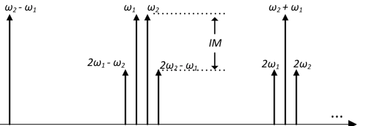
Most of the PAs operate near to the 1 dB compression point in order to achieve higher efficiency, but it suffers from distortion of the higher order harmonics. Such requires that the power of the higher harmonics should be below at least 30 dBm from the power of the carrier frequency, i.e., -30 dBmc. This undesired harmonics may corrupt the signal of interest and can be classified as:
• Harmonics of the carrier frequency: fh=n fc.
• IM products: fI M =n f1±m f2.
...
ω1
ω
2ω1
3ω1
Figure 2.3: Spectrum of the output voltage with harmonics effect.
...
ω1 ω2
2ω2 - ω1 2ω1 - ω2
ω2 + ω1
2ω1 2ω2
ω2 - ω1
ω
IM
Figure 2.4: Spectrum of the output voltage with the respective intermodulation products.
In the case of the two-tone test, the order of an IM product can be determined bynandmcoefficients, where this two coefficients are integers, resulting in
order(I M) =n+m. (2.10)
Therefore, in the case of the 3rd order IM (I M3) the products are: 2ω1+ω2, 2ω1− ω2, 2ω2+ω1and 2ω2−ω1.
The simple way to measure the total distortion of the amplifier with a single-tone test, besides the 1 dB CP and IP3, is through the total harmonic distortion (THD). Whenever the amplifier operates in non-linear region it generates an extra number of harmonics, which may distort the signal of interest.
THD=
n ∑ i=2
Pi
P1 . (2.11)
2.4
Transmitter
Modulator
RF BPF RF BPF
PA
Transmitter
LNA
RF BPF RF BPF
Demodulator Receiver Signal
Information
Signal Information
Up-converter
Down-converter
LO
LO
Figure 2.5: Simplified block diagram of the transmitter (top) and receiver (bottom) for wireless communication.
2.4. TRANSMITTER
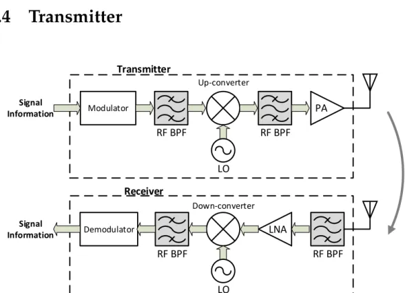
Since in the wireless communication systems there is no transmitter without the receiver, it is shown in Figure 2.5 the block diagram of the receiver and transmitter to give an overall idea of the complete wireless transceiver.
Giving more emphasis to the transmitter, there are two typical architectures: Heterodyne upconversion and Direct upconversion. Each of them has a digital signal processor (DSP), digital-to-analog converter (DAC), Mixers (represented by X symbol), local oscillator (LO) and PA.
2.4.1
Heterodyne Upconversion
The heterodyne upconversion architecture, sometimes called as 2-step upconver-sion, is the most often used in the transmitters, represented in Figure 2.6. Since in nowadays systems transmit data in the form of quadrature baseband signals, the transmitter must be able to processes this signal. As a result, the signal is processed in the DSP where signal is split into the in-phase,I, and quadrature,Q, channels. These are converted to analog trough DAC and latter are upconverted to the RF signal, carrier frequency.
This architecture, in particular, has distinction in using the intermediate fre-quency (IF) to process quadrature modulation, up-converting toωIF+ωLO,
usu-ally using two mixers and two LO signals with phase differentiated by 90o. Then, first bandpass filter (BPF) suppresses the IF harmonics, while the second BPF removes the unwanted mirrored sideband,ωIF−ωLO. This architectures brings as
the main advantage not having LO pulling, compared with the direct upconversion [6, 7].
IF BPF RF BPF
PA
Up-converter
LO
DSP
DAC
DAC
-90
oLO I
Q
2.4.2
Direct Upconversion
Direct upconversion transmitter, can be also called as homodyne upconversion, is defined principally by having its carrier frequency equal to the LO frequency. By this means that the signal from the baseband is directly upconverted to the carrier frequency. This architecture is shown in Figure 2.7, which seems to be very simple, but this presents a drawback of introducing LO pulling. In other words, putting the PA close to the LO, in terms of frequency domain, causes injection of the PA noise into the spectrum of the LO, which may stay "locked" if the noise increase. However, modern direct conversion have tried to alleviate this effect by moving the output spectrum of the PA far from the LO frequency [6, 7].
HF BPF
DSP
DAC
DAC
-90
oLO
PA I
Q
Figure 2.7: Block diagram of the Heterodyne transmitter.
C
H
A
P
T
E
R
3
P
OWER
A
MPLIFIERS
There are many ways to classify the power amplifiers, but the most important is by their class of operation, which essentially depends on trade-off between linearity, efficiency, signal gain and output power of the PA.
There are classes named alphabetically from A to T and they can be lumped into two basic groups: conventional amplifiers (A, AB, B and C) and switching mode amplifiers (D, E, F . . . ). The last group is mostly preferred by the wireless systems, despite of its amplitude non-linearities, because those amplifiers can achieve higher efficiency. Amplitude linearity is not necessarily needed, since phase modulation is greatly used by these systems. As a consequence, the ampli-tude non-linearities do not affect those wireless systems, but phase linearity does, and non-linear amplifiers can provide that [2].
The following sections describe those two groups in some detail, bearing in mind that the design of the RF power amplifier assumes CMOS technology, MOS transistors and its equations are used to explain each class operation. But that does not mean that the classes operation are not adaptable to a different technology.
3.1
Conventional Amplifiers
L
1M
1V
inMatching Network
R
LBiasing
ID
Io
C
blockV
DDFigure 3.1: Classical RF PA with inductive load
within the group of conventional amplifiers, turning the conduction angle into a concept with great importance. The conduction angle,θ, varies between 0 and 2π
(or in degrees: between 0 and 360), and defines the duration of the period in which the given transistor is conducting, where 2π(or 360o) corresponds to the full cycle of conduction.
All these classes, named alphabetically from A to C, can be implemented using the same circuit, depicted in Figure 3.1, where Cblock is a DC blocking capacitor,
L1is a load inductor,RL represents load impedance of the antenna andM1is an
output transistor that operates as a controlled current source. The bias voltage at the gate is the one that allows to shape the current conduction angle and therefore differentiate those classes. A load inductor is preferred over a resistor, because if the radio-frequency choke (RFC) inductor is used the voltage drop trough this inductor will be practically zero. The RFC inductor is also desired because of its definition of passing DC current and blocking everything else. For that purpose, the RFC must have large enough inductance in order to pass DC current ripple and block or reduce significantly the alternating current (AC) current ripple.
3.1.1
Class-A
3.1. CONVENTIONAL AMPLIFIERS
off, i.e. it will conduct during all of its conduction angle, which is 360o. This is why, between all the classes, this one is the most linear. The CMOS transistor must operate in the active region (saturation region) and so its drain current is given by the square law
iD = 1
2Kn(
W
L)(vGS−Vth)
2 f or v
GS ≥Vth and vDS ≥vGS−Vth, (3.1)
where LandW are the channel length and width of the transistor, respectively,
vGSis gate-to-source voltage,Vthis the threshold voltage,vDSis drain-to-source voltage and
Kn =µn0Cox, (3.2)
whereµn0is the low-field surface electron mobility in the channel,Cox =ǫox/tox
is the oxide capacitance per unit area of the gate,tox is the oxide thickness,ǫox =
0.345 pF/cmis the silicon oxide permittivity [5].
Typically it is used the topology shown in Figure 3.1 with the addition of a LC parallel-resonant circuit (as illustrated in Figure 3.2 by Lo and Co) and also
a coupling capacitor Cc, which may be included in the matching network. The
parallel-resonant circuit is used for the narrowband Class-A RF PA to suppress the undesired harmonics and filter the narrowband spectre of the signal. Although this is not need for the wideband power amplifiers. In its turn, the coupling capacitor, which is also known by DC-blocking, ensures that only AC current is flowing through the load resistorRL.
Supposing that the AC input signal is a sinusoidal wave, the output voltage will have a sinusoidal wave too and the power in the load, or output power, will be given by
Po = V 2 o
2RL, (3.3)
whereVo is the amplitude (or peak value) of the sinusoidal output voltage.
Recall-ing the formula of the drain efficiency:
ηd = Po
Pdc, (3.4)
and having into account that the maximum drain efficiency occurs at the maximum output power, which in turn is maximum at the maximum output voltage, since
the value of the RL is a constant. Maximum output voltage occurs when the
transistor drain current is almost zero, considering ideal components, whereL1
inductance is an RFC and then the current from the supply will flow completely
L
1M
1V
inV
DDMatching
Network
R
LC
CBiasing
ID
I
oLo Co
C
CR
optFigure 3.2: Class A stage
maximum theoretical drain efficiency results into 50 % [9], as demonstrated in Equation (3.5).
ηd(max)(%) =100×V
2
o(max)/(2RL)
VDDIDC =
100×1
2
Vo(max) VDD
!2
=50 %. (3.5)
The drain current can be expressed as
iD = ID +id = ID+Ipk·cos(θ), (3.6)
whereID is the DC component of the drain current,idis the AC component of the
same and its peak amplitude is defined by Ipk.
The drain current and drain-to-source voltage are represented in Figure 3.3, that considers maximum voltage swing (by ignoring pinch-off voltage, which defines the division between the saturation and the linear region of the transistor) and ideal components, where
ID(max) =2·Ipk(max) =2·IDC, (3.7)
3.1. CONVENTIONAL AMPLIFIERS
Current Voltage
2θ(degrees)
0 90 180 270 360 450
ID(max)
VDS(max)
Figure 3.3: Class-A ideal drain voltage and current waveforms
By a proper managing of the Equations (3.7) and (3.8) into a general equation of the output power capability it results into
cp =
Po(max)
VDS(max)ID(max) =
1 2 ·
Vo(max)Io(max) VDS(max)ID(max) =
1
8 =0.125. (3.9)
To sum up, the Class-A RF power amplifiers can achieve high linearity, produc-ing an amplified replica of the input voltage or current waveforms, at the expense of poor efficiency.
3.1.2
Class-B
Higher efficiency is achieved by reducing the conduction angle, i.e., transistor do not conduct the drain current all the time. This way, the power dissipation of the transistor is reduced, since the multiplicative factor of the drain-to-source voltage by the drain current is decreased.
The Class-B RF power amplifiers is the category on which the transistor con-ducts only during half of its period, or by other words, the drain current waveform has a conduction angle of 180o and so has a sinusoidal wave during only for half of its period. To achieve that, the transistor must be biased close to the thresh-old voltage value (Vth), so that the transistor can exchange its operation quickly between cut-off and active region.
It can be designed with the same topology of the Class-A, with high QLC
using two transistors instead of one, with each of them delivering a half sinusoidal voltage and the transformer will recover the full sinusoid at the load.
Like in Class-A amplifier, the maximum peak value of the output voltage reachesVDDand leads to the maximum drain efficiency of 78.5 %, which also can
be calculated as follows (further demonstration can be seen in [5]):
ηd(max)(%) =100× V
2
o(max)/(2RL)
2Vo(max)VDD/(πRL) =100× π
4
Vo(max) VDD
=100×π
4
VDD
VDD =100×
π
4 =≃78.5 %.
(3.10)
The maximum drain current, in this case, increases by a factor ofπrelatively to the supply current, IDC, but the maximum drain-to-source voltage remains twice
of theVDD.
ID(max) =2·Ipk(max) =π·IDC, (3.11)
VDS(max) =2·Vo(max) =2·VDD. (3.12)
Under the same considerations mentioned at the Class-A definition, the drain current and the drain-to-source voltage of the Class-B RF power amplifier are presented in the Figure 3.4.
Current Voltage
2θ(degrees)
0 90 180 270 360 450
ID(max)
VDS(max)
Figure 3.4: Class-B ideal drain voltage and current waveforms
As the relation between VDS(max),ID(max) and Vo(max)Io(max) did not change comparatively to the Class-A, the output power capability of the Class-B RF power amplifiers remains the same
cp =
Po(max)
VDS(max)ID(max) =
1 2·
Vo(max)Io(max) VDS(max)ID(max) =
1
3.1. CONVENTIONAL AMPLIFIERS
The efficiency is improved, however there are always drawbacks together with the benefits. The turning off the transistor creates higher undesired harmonics, as well as the transistor becomes less linear. In the Class-A it was referred to the use of the parallel-resonant circuit, but it takes more importance now. Thus, higher quality of these components is desired in order to better suppress those harmonics, which can be calculated as follows:
Lo =
Ropt
QL·ωo
, (3.14)
Co = QL
Ropt·ωo, (3.15)
whereQL is loaded quality of the parallel-resonant circuit at frequency of work, ωo, andRopt is an optimum value for the desired output power before matching.
3.1.3
Class-AB
The Class-AB RF power amplifiers, as the name suggests by itself, is the category which fits between the Class-A and Class-B and therefore its conduction angle is in the range of 180o to 360o, as well as the efficiency lays between 50 % and 78.5 %. This category allows to choose the better trade-off between the efficiency and linearity, i.e., a power amplifier that could be more linear than the Class-B and more efficient that the Class-A.
The waveforms of the drain current and drain-to-source voltage that exemplify Class-AB RF power amplifiers operation is showed in Figure 3.5
Current Voltage
2θ(degrees)
0 90 180 270 360 450
ID(max)
VDS(max)
Further equations are presented in Section 3.1.4, Class-C, as they are common to both Class-AB and Class-C power amplifiers, since it is only the range of the conduction angle that differentiates them from what they are.
3.1.4
Class-C
The last category of the conventional power amplifiers, and the less linear, is the Class-C. This one has its transistor biased to operate mostly in the cut-off region and therefore its conduction angle is below 180 %. This one is even more efficient than the previous classes, which reaches efficiency range from 78.5 % to 100 %. For some applications it is desirable to have more efficiency in exchange of its linearity. The radio station could be an example, which need to transmit large powers with an efficient operating mode.
The maximum drain and maximum drain-to-source voltage in function of conduction angle are
ID(max) =Ipk(max)·2π·1−cos( θ
2)
θ−sin(θ). (3.16)
An example of the drain current and drain-to-source voltage waveforms are illustrated in Figure 3.6.
Current Voltage
2θ(degrees)
0 90 180 270 360 450
ID(max)
VDS(max)
Figure 3.6: Class-C ideal drain voltage and current waveforms
The maximum drain efficiency,ηD(max) is now in function of conduction angle [9], as given by
ηD(max)(%) =100× θ−sin(θ)
4·
sin(θ2)−θ2·cos(θ2)
3.2. SWITCHING AMPLIFIERS
whereθis the conduction angle, the equalityVDS(max) =2VDD and zero pinch-off voltage are still taken into account. This function is also valid for other conven-tional classes.
In the same way, output power capability can be calculated,
cp = 1
8π ×
θ−sin(θ)
1−cos(θ2). (3.18)
The drain efficiency and the output power capability functions are shown through a plot in Figure 3.7.
cp ηD θ(degrees) Class-B Class-A Class-AB Class-C P ow er C ap ab il li ty , cp D ra in E ffi ci en cy , ηD (% )
0 180 3600
0.02 0.04 0.06 0.08 0.1 0.12 0.14
50 60 70 80 90 100
Figure 3.7: Drain efficiency and power capability in function of conduction angle
Analysing this plot (Figure 3.7), it is possible to sum up what already have been told in these sections, that is: conventional classes are categorized in function of conduction angle, and as it decreases the efficiency is increased. But at the same time, the output power capability decreases, which also means that the maximum output power decreases too. So, there will be always a trade-off between efficiency, output power and linearity.
3.2
Switching Amplifiers
the off state, the transistor operates in cut-off region and opposite waveforms are acquired, i.e. drain current is zero and drain-to-source voltage is determined by load circuit [5]. In the ideal cases, where the transistor behaves like an ideal switch and ideal passive components are considered, there is no overlap in time between the current and voltage, and so there is no power dissipation, which leads to 100 % of drain efficiency. Of course that happens only theoretically, because there are no ideal components in practice, even so, this group of amplifiers are much better when high efficiency is needed.
In this section, the most "popular" switching power amplifiers will be discussed, such as Class-D, Class-E and Class-F. As the Class-E RF power amplifiers are the main object of this thesis it will be discussed in more detail in Chapter 5, a chapter dedicated only to its theoretical study and its design. Even so, a brief analysis of Class-E is described in this chapter.
3.2.1
Class-D
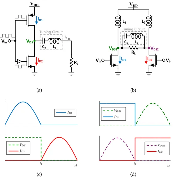
Class-D power amplifiers can be classified into two groups [10]:
• voltage-mode Class-D (VMCD) with series-resonant circuit;
• current-mode Class-D (CMCD) with parallel-resonant circuit.
Typically, both groups use two transistors that operate in a push-pull switching pair and very similarly to an CMOS inverter. The VMCD produces voltage across transistors with square wave and half-wave sinusoid current. In case of the CMCD opposite is produced: a square wave current and half-wave sinusoid voltage. Both transistor are driven by a square input wave and the output signal is tuned to the fundamental frequency. The circuit topology for each Class-D mode and its principal waveforms are represented in Figure 3.8.
In [5, 11, 12, 13] detailed study and comparison between them two are made. Their theoretical analysis and implementation made possible to conclude that whereas the VMCD has the inability to work at high-frequencies, the CMCD can achieve higher frequencies with help of ZVS condition, the one that makes a huge influence in Class-E, as it will be seen in shortly. This inability of the VMCD occurs because the parasitic reactances induced by the two transistors lead to substantial power loss at higher frequency.
3.2. SWITCHING AMPLIFIERS
Vin
VDD
RL
Io
Co Lo
Tuning Circuit VDS ID2 ID1 (a) Vin RL
Co Lo
Tuning Circuit
Vin
L1 L2
VDD VDS1 ID2 ID1 VDS2 (b)
ID2
VDS
ωt ID1
t1
(c)
ID2
VDS2
ωt ID1
VDS1
t1
(d)
Figure 3.8: The Class-D power amplifiers: (a) VMCD, (b) CMCD and their respec-tive currents and voltages
3.2.2
Class-E
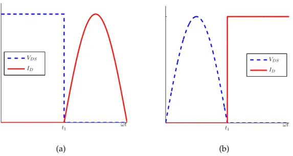
Class-E power amplifiers has the same functions of the Class-D, though using only one transistor. There are two types of Class-E as well: zero-voltage switching (ZVS) and zero-current switching (ZCS). More detailed information about them and their equation are discussed in Chapter 5. The most basic circuit of this class in ZVS mode is shown in Figure 3.9.
that the capacitanceC1is used in ZVS mode, allowing a soft-switching. A hard-switching happens in ZCS mode, where abrupt voltage drop through the transistor occurs from high value to zero, this causes a lower efficiency in the ZCS mode, and therefore, the ZVS is more preferable. Given these points, the design of the shunt capacitanceC1plays a big role, when it comes to avoid power loss on the transistor
[14]. This capacitance absorbs, so to speak, the voltage through the transistor when it is on, and this way, avoids overlapping between voltage and current waves, consequently, minimizes the product voltage-current. Ideally this product would be always zero and hence, there would be no power dissipation, leading to the efficiency of 100 %.
TheVBiasingvoltage represented in Figure 3.9 plays a big role, because it defines
theVGSvoltage of the transistorM1and consequently defines its operation region.
L
1M
1V
inR
LV
DDC
oL
oC
1Tuning Load Circuit
IDC
ID
Io
jX
IC
V
BiasingC
blockFigure 3.9: Basic topology of the ZVS Class-E power amplifier.
3.2.3
Class-F
3.2. SWITCHING AMPLIFIERS
circuit, respectively. This way, the undesired harmonics are eliminated and only a fundamental harmonic is seen at the load.
L1
M1
Vin
RL
VDD
IDC
ID Io VBiasing
Cblock
3fo 5fo nfo
Cblock
Lo Co Tuning Load Circuit
Figure 3.10: Basic topology of the Class-F power amplifier.
If open circuits are chosen for the odd harmonics, as represented in Figure 3.10 by 3fo, 5fo, ...n fofilter blocks, the square wave is obtained for the output voltage.
The load network on this case is defined by parallel-resonantLoCoRL circuit tuned
to the operating frequency fo andnnumber of parallel-resonant circuits tuned to
thennumber of odd harmonics, all of them connected in series. This implies that the parasitic impedances of the transistor end up in parallel with short-circuits, making them negligible [15].
If the opposite is chosen, i.e., short circuit for the odd harmonics, the square wave is obtained for the output current. This results in a zero impedance in each resonant circuit and an infinite impedance at even harmonics [14]. But, usually, the square voltage is preferred.
ID
VDS
ωt t1
(a)
ID VDS
ωt t1
(b)
Figure 3.11: The Class-F drain current and drain-to-source voltage: (a) square voltage, (b) square current.
3.3
Current Source Versus Switched-Mode
Operation
Unwilling to seem redundant, the difference between these two modes of operation is mainly the same as the difference between a switch and an high impedance current source. Typically, Class-A and Class-B topologies are considered as linear PA’s, despite, not just they lack consistency, but also they keep modelling for small-signals approaches of amplifiers that operate in the large-signal regime. In this subsection, the differentiation between the current source and switched-mode operation, in terms of their large-signal currents and voltages, will be made. Furthermore, it will be possible to divide the current source into pulse-current (PU) operation and continuous wave (CW) operation, as was differentiated by the group of the conventional amplifiers. The most important difference between both modes of operation (current source and switch) during conduction, is the range of voltages that are available on the transistor [16].
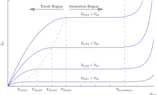
• Working in switched-mode: the transistor is cycled between triode region
(low impedance conduction) and cut-off (that is an high impedance state) (more about the transistor operating regions can be seen in Appendix B).
– When VDS ≤ (VGS−Vth), for ID 6= 0, is possible to enter the triode
3.3. CURRENT SOURCE VERSUS SWITCHED-MODE OPERATION
VGS1> Vth
VGS2> Vth
VGS3> Vth
ID
VDS
Saturation Region Triode Region
VGS4> Vth
VDsat1 VDsat2 VDsat3 VDsat4 Vbreakdown
Figure 3.12: Characteristic curves of drain current versus drain-to-source voltage.
In low impedance conduction, the voltage through the transistor,VDS,
is as low as possible.
– When the device is cut-off, means that the voltage can freely cross the horizontal axis while the current remains zero.
• Operating as a current source: the transistor can be driven in the two modes of conduction presented early, the continuous or the pulse-current one.
– For the CW conduction, the device is biased at a finite current and
voltage. From there, as long as the triode region is avoided, withVDS
preventing to reach breakdown voltage,VDS and ID are free to assume
any non-zero value.
3.4
Discussions
To conclude the overview on RF power amplifiers, in Table 3.1 are presented the relevant characteristics of the discussed PA classes.
Table 3.1: Most important characteristics of the linear and switching mode power amplifier classes.
Class-A Class-AB Class-B Class-C
Conduction Angle(o) 360 180∼360 180 0∼180 Ideal Efficiency,ηd(%) 50 50∼79 79 79∼100
Linearity Good Good Moderate Weak
Maximum Power Capability 0.125 0.134 0.125 0.125
Gain Large Large Moderate Low
Class-D Class-E Class-F
Ideal Efficiency,ηd(%) 100 100 100
Linearity poor poor poor
Gain small small small
C
H
A
P
T
E
R
4
C
LASS
-A P
OWER
A
MPLIFIER
Class-A is the simplest power amplifier, not only because of its simple design, but also because of its simple implementation. Moreover, the understanding of its operation mode and of its design is crucial to comprehend all other classes, which originate from this basic design with addition of some specific biasing, driving or tuning circuits.
This chapter has no intention to repeat the theory of the Class-A, as it was discussed in the previous chapter, but it aims to present a simple design and implementation of the Class-A, with and without real reactive components. The main focus is given primarily to the comparison of the simulation results using ideal LC components and using real models. In this regard, Planar Inductor RF and Planar MIM Capacitor RF models are used. This type of RF power amplifier is implemented in 130 nm CMOS technology with voltage supply of 1.2 V at frequency of 2.4 GHz.
4.1
Implementation of the Class-A Power Amplifier
4.1.1
Design of Class-A Power Amplifier
The amplifier design consists in a basic single-ended PA with a common source accomplished by an inductive load. To properly set the DC conditions, a current mirror is used as biasing circuit. Circuit schematic is shown in Figure 4.1.
L
1M
BR
BR
BlM
1V
inR
LC
blockC
mL
mOutput Matching
IB
I1
ID
V
DD Biasing CircuitV
DDIo
Figure 4.1: Basic Class-A PA with circuit biasing and output matching
Table 4.1: Class-A PA specifications
Specifications Value
VDD 1.2 V
fo 2.4 GHz
GP ≥10 dB
Zout 50Ω
Pout [0∼20] dBm
As a starting point, it was decided to establish the biasing factor of the circuit.
To minimize the current consumption, the biasing transistor MB is sized to be
smaller than the PA transistor, hence the biasing factor is taken as 10:1, which implies the same current ratio, as presented in Equation (4.1).
IB = ID
10. (4.1)
4.1. IMPLEMENTATION OF THE CLASS-A POWER AMPLIFIER
by sizing drain current, ID, that were set at 200 mV and 10 mA, respectively.
WM1= 2
IDLM1
KNVDsat12 . (4.2)
Therefore, this scaling has led to the transistors design presented at Table 4.2 (assuming same length for both transistors:L =Lmin =120nm).
Table 4.2: Transistor’s design
Transistor Width[µm] ID[mA] VDsat[mV]
M1 120 10 200
Mbias 12 1 200
Initially, it was used an ideal inductive load. The purpose of this inductor is to behave like an AC open circuit at work frequency, so it can carry a constant current. Henceforth, its L parameter must be sufficiently large but well designed in order to cancel the circuit’s resonance. Bearing that in mind, the imaginary part of itself plus the parasitic capacitances of transistor M1should be nullified, which is possible to achieve with Equation (4.3). The blocking capacitor is also wanted to be large enough to prevent DC passage and allow to pass only AC.
ωo = √1
L·C. (4.3)
Finally, the output matching must be designed in order to adapt the PA signal to the antenna’s impedance,RL, which also allows efficiency improvement, since it yields to lower reflection losses. For that purpose, the LC mesh was considered (Inductor in parallel and capacitor in series), as showed in Figure 4.1. Before that, the output impedance of the PA must be found in order to calculate the appropriate values for the LC mesh.
The circuit from Figure 4.1 (ignoring the output matching circuit) can be easily redesigned to its small signals form, by nullifying DC voltages, short-circuiting the blocking capacitors and introducing parasitic capacitors, which work at high frequencies Figure 4.2. Analysing the impedance seen from the output, shunting
the input source, which impliesVgs1 = 0, through Kirchhoff’s Current Law the
output currentioutis given by Equation (4.4),
iout =vout
1
jωL1 +jωCds1+
1
rds1 +jωCgd1
rds1
gm vgs1 cds1 L1
cgs1
cgd1
vin vout
Zout
iout
vgs1
Figure 4.2: Small signal circuit of the classic PA.
From Ohm’s Law, rewriting the previous equation as Zout = vout/iout, the
output impedance expression leads to (4.5).
Zout= 1
1
jωL1 +jωCds1+ 1
rds1 +jωCgd1
. (4.5)
Regarding to the LC mesh illustrated in Fig. 4.3, its input impedance Zm is
given by (4.6).
Class-A PA
(w/o matching)
Class-A PA
(w/o matching)
Output Matching
Z
outZ
mC
mL
m
R
L
Figure 4.3: LC matching network
Zm =Cm+
Lm·RL
Lm+RL
. (4.6)
To summarize, the real part ofZm andZoutexpressions must be equal, and the
4.2. SIMULATIONS RESULTS
system solution in Equation (4.8) allows to obtain the Lm andCm values, which
are presented in Table 4.3.
ℜ{Zout}+ℑ{Zout} =Zm ⇔ (4.7)
⇔
Cm =
L2mω2o+R2L
Im{Zout}L2mω3o+Im{Zout}R2Lωo+LmR2Lω2o
,
Lm =
RLpRe{Zout}
p
RLω2o −ω2oRe{Zout}
.
(4.8)
Table 4.3: Design of the parameters L and C
Parameter Value
L1 7.58 nH
Lm 5.395 pF
Cm 2.24 pF
4.2
Simulations Results
The simulations analysis of PA design were performed using the SpectreRF engine from Cadence Design Systems. For validation purposes of Class-A PA designed, operating at 2.4 GHz, four types of analysis were verified at output stage. The S-parameter simulation was performed to generate plots of the return losses (S22), small signal gain (S21) and noise figure (NF). For large signal analysis to
measure output power levels, 1 dB compression point and power added efficiency (PAE), the periodic steady state (PSS) simulation were performed. The third order intercept point (IP3) plot was given by the Periodic AC (PAC) simulation. Lastly, the transient simulation was performed to plot the output voltage and current, used to measure the DC power consumption and conduction angle.
In the Section 4.1.1, the PA was designed considering ideal components. How-ever, it is important foresee its real behaviour, therefore it is also presented a simulation result based on real models. The schematics taken from Cadence tool for the A simulation with ideal LC components, as well as for the Class-A simulation with real models LC components are presented in Class-Appendix Class-A.1, where variables of the ports, presented in Appendix A.3, were set as follows: