Ricardo Filipe Soares Rodrigues
Licenciado em Ciências da Engenharia Electrotécnicae de Computadores
Design of a Class-D RF power amplifier in
CMOS technology
Dissertação para obtenção do Grau de Mestre em Engenharia Electrotécnica
Orientador:
Prof. Dr. João Pedro Abreu de Oliveira, Prof. Auxiliar,
Universidade Nova de Lisboa
Júri:
Design of a Class-D RF power amplifier in CMOS technology
Copyright cRicardo Filipe Soares Rodrigues, Faculdade de Ciências e Tecnologia,
Uni-versidade Nova de Lisboa
A
CKNOWLEDGEMENTS
Gostaria de começar por agradecer à Faculdade de Ciências e Tecnologia da Universidade Nova de Lisboa, por toda a aprendizagem, quer a nível académico, quer a nível pessoal. Estas competências adquiriras serão certamente de extrema importância para o meu futuro profissional.
Agradeço deste modo ao Prof. João Pedro Oliveira, por ter aceite ser o meu orientador e me ter proporcionado um tema de tese interessante e muito atual, que me obrigou a trabalhar fora da minha área de conforto, quero também agradecer por todo o apoio e por tudo o que me ensinou, não só no âmbito da realização desta tese, mas também durante todo o curso.
Ao longo deste curso, houve muitos professores, dentro e fora do departamento de Electrotecnia, que me marcaram, queria, portanto agradecer a todos eles, que me proporcionaram não só imensos conhecimentos mas também muitos bons momentos, dentro e fora das salas de aulas.
Quero agradecer aos meus colegas da faculdade, em nenhuma ordem em particular, Rúben Carvalho , Fábio Vidago, Filipe Rodrigues, Filipe Viegas, Carlos Oliveira e Élvio Mendes, Ricardo Neto, Rodrigo Fraústo. Muito obrigado por todos os momentos.
A
BSTRACT
In this thesis an RF Class-D Power Amplifier is presented. The analysis of the Class-D amplifier considering ideal components has shown that the drain efficiency of 100% can be achieved. The output power and the drain efficiency are degraded by the internal resistance of each component. A driver is used to drive the gate capacitances of the Class-D amplifier. Both driver and amplifier are implemented with CMOS inverters. The size of the inverters in the driver is scaled down by a factor of 3 relatively to the preceding stage. The first being the inverter of the Class-D amplifier. At the output a 3rdorder Butterworth
bandpass filter is implemented. A non-ideal analysis of the Class-D amplifier is performed to create a base model which is used to aid in the design of the circuit.
The RF Class-D Power Amplifier with the operation frequency of 2.4GHz was im-plemented with standard 130 nm CMOS technology. Two simulations were taken into account considering ideal and pre-layout components in the output filter. The following results were obtained when using ideal components: the output power of 6.91 dBm, the drain efficiency of 40% and the overall efficiency of 23%. Using pre-layout components the results were the following: the output power of 0.317 dBm the drain and overall efficiency of 8.6% and 4.9%, respectively.
Keywords: Class-D, RF power amplifier, CMOS, drain efficiency, radio-frequency,
R
ESUMO
Nesta tese um amplificador de potência Classe-D para aplicações de rádio frequência é apresentado. A análise do amplificador Classe-D considerando componentes ideais mostrou uma eficiência de dreno de 100% pode ser alcançada. A potência de saída e a eficiência de dreno podem ser degradadas pela resistência interna dos componentes. Umdriveré usado para fornecer corrente necessária ao amplificador Classe-D. Tanto o drivercomo o amplificador são implementados com inversores emCMOS. O tamanho dos inversores dodriversão escalados por um factor de 3 em relação ao inversor precedente. A
factor de escalamento é feito a partir do inversor do amplificador. À saída do amplificador é implementado um filtro passa-bandaButterworthde 3 ordem. Uma análise não ideal do
amplificador é realizada para cria um modelo base utilizado para o dimensionamento do circuito.
O amplificador Classe-DRFcom uma frequência de operação de 2.4 GHz foi
imple-mentado em tecnologiastandard CMOSde 130 nm. Duas simulações foram realizadas, uma
considerando componentes ideais e a segunda considerando componentes depre-layout
no filtro de saída. Foram obtidos resultados na simulação considerando componentes ideais: potência de saída de 6.91 dBm eficiência de dreno de 40% e uma eficiência global de 23%. Usando componente depre-layoutos seguintes resultados foram obtidos: potência
de saída de 0.317 dBm eficiência de dreno de 8.6% e uma eficiência global de 4.9%.
Palavras-chave: Classe-D, amplificador de potência RF,CMOS, eficiência de dreno,
C
ONTENTS
List of Figures xv
List of Tables xvii
1 Introduction 1
1.1 Background and Motivation . . . 1
1.2 Thesis Organization . . . 2
2 RF Power Amplifiers Overview 3 2.1 RF Power Amplifiers . . . 3
2.1.1 Linear Amplifiers . . . 4
2.1.2 Non-Linear Amplifiers . . . 8
2.2 Definition of Output Power . . . 13
2.3 Amplifier Efficiency . . . 14
2.4 Transmitter Architectures . . . 16
2.4.1 Heterodyne Transmitters . . . 17
2.4.2 Direct Up-conversion Transmitter . . . 17
2.4.3 Direct Digital Conversion . . . 18
2.4.4 Sigma-Delta Direct Digital Conversion . . . 18
2.5 Transmission Modulation Technique Example:Bluetooth. . . 19
3 RF Class-D Power Amplifier With Sigma-Delta Modulation 23 3.1 MOSFET as a Switch . . . 24
3.2 CMOS Inverter . . . 26
3.3 Class D Voltage-Switching Power Amplifier . . . 27
3.3.1 Ideal Analysis . . . 27
3.3.2 Non-Ideal Analysis . . . 30
3.3.3 Gate Driver . . . 32
3.4 Series-Resonant Circuit . . . 34
3.5 Sigma-Delta Modulation . . . 36
3.5.1 Noise Shaping due to Oversampling . . . 36
3.5.2 First order Sigma-Delta . . . 38
CONTENTS
4.1 Class-D PA High-Level Model . . . 41 4.2 Pre-Layout Simulation Model . . . 47 4.3 RF Class-D PA With Sigma-Delta Modulator . . . 52
5 Conclusion and Future Work 55
5.1 Conclusion . . . 55 5.2 Future Work . . . 56
Bibliography 57
A Butterworth Bandpass Filter Design Tables 61
B Ideal 1st Order∑ ∆Modulator Block. 63
L
IST OF
F
IGURES
2.1 Power amplifiers groups and classes. . . 4
2.2 Linear power amplifiers schematic . . . 5
2.3 Class-A amplifier drain current waveform for two periods. . . 6
2.4 Class-B amplifier drain current waveform for two cycle. . . 6
2.5 Class-C amplifier drain current waveform for two cycles. . . 7
2.6 Class-D-1power amplifier schematic. . . . 9
2.7 Class-D-1transistorM 1voltage and drain current waveforms. . . 9
2.8 Class-D-1transistorM 2voltage and drain current waveforms. . . 10
2.9 Class-E power amplifier schematic. . . 10
2.10 Class-E voltage and drain current waveforms. . . 11
2.11 Class-F power amplifier schematic with 5th harmonic peaking. . . 11
2.12 Class-F voltage and drain current waveforms. . . 12
2.13 Class-F-1power amplifier schematic with 5th harmonic peaking. . . . 12
2.14 Class-F-1voltage and drain current waveforms. . . . 13
2.15 Definition of power output. . . 13
2.16 DC power consumption . . . 15
2.17 DC power consumption including driver stages. . . 15
2.18 Heterodyne transmitter. . . 17
2.19 Direct up-conversion transmitter. . . 17
2.20 Block diagram of a direct digital up-converter. . . 18
2.21 Block diagram of a direct digital up-converter using a Sigma-Delta DAC. . . . 19
2.22 BluetoothModulation Schemes. . . 21
3.1 Small-signals models. (a) Simplified triode-region model for a smallVDS. (b) MOSFET model when is turned off. . . 25
3.2 CMOS inverter schematic. . . 26
3.3 CMOS inverter transfers characteristics. . . 26
3.4 A CMOS CDVS PA with a series-resonant circuit. . . 27
3.5 Waveforms of a CDVS PA. . . 28
3.6 Cascade of inverters used to drive a big capacitance. . . 33
3.7 Bandpass filter frequency response. . . 34
LIST OFFIGURES
3.9 ∑ ∆Modulator. . . 36
3.10 Ideal n-bit ADC quantization erroren. . . 37
3.11 Frequency Spectrum of a input signalSin and quantization noise. . . 37
3.12 First order ADC∑ ∆modulator. . . 39
3.13 Signal and Noise Spectrum . . . 39
4.1 High-level model circuit of the RF CDVS PA. . . 41
4.2 Power output in function of PMOS width(equation 4.6). . . 44
4.3 Power output in function of NMOS width (equation 4.6). . . 44
4.4 Overall efficiency in function of the PMOS width(equation 3.30). . . 46
4.5 Schematic of the CMOS driver and CDVS PA circuits. . . 47
4.6 RF CDVS PA circuit waveforms. . . 49
4.7 Output power spectrum using a filter with ideal components. . . 51
4.8 Output power spectrum using a filter with pre-layout components. . . 51
4.9 ∑ ∆modulator with the RF CDVS PA circuit. . . 52
L
IST OF
T
ABLES
2.1 Transistor conduction angle. . . 5
2.2 Efficiency of the linear amplifiers. . . 8
2.3 BluetoothClasses. . . 19
2.4 BluetoothACPR requisites. . . 20
2.5 BLE chipsets current consumption. . . 21
2.6 BLE Output Power requisites. . . 22
4.1 Transistors Parameters. . . 42
4.2 Series-resonant circuit parameters. . . 42
4.3 Internal resistance and width of the PMOS and NMOS. . . 43
4.4 High-level model RF CDVS PA design results. . . 45
4.5 Transistor width of the inverters’ stages. . . 48
4.6 3rdorder Butterworth bandpass filter values. . . . 48
4.7 RF CDVS PA results considering ideal analysis, high-level model and the simulation model using a filter with ideal and pre-layout components. . . 50
A.1 Normalized ButterworthRSource =1,RLoad =1 [p. 58][36]. . . 61
G
LOSSARY
∑ ∆ Sigma-Delta.
BLE BluetoothLow Energy.
CDVS Class-D Voltage-Switching.
CMOS Complementary Metal-Oxide-Semiconductor.
DC Direct Current.
DPSK Differential Phase-Shift Keying.
DQPSK Differential Quadrature Phase-Shift Keying.
GFSK Gaussian Frequency-Shift Keying.
IC Integrated Circuit.
IoT Internet of Things.
ISM Industrial Scientific Medical.
MIM Metal-Insulator-Metal.
MOSFET Metal-Oxide-Semiconductor Field-Effect Transistor.
NMOS N-type metal-oxide-semiconductor.
PA Power Amplifier.
PAE Power Added Efficiency.
PMOS P-type metal-oxide-semiconductor.
PSK Phase Shift Keying.
RF Radio Frequency.
GLOSSARY
ZCS Zero Current Switching.
C
H
A
P
T
E
R
1
I
NTRODUCTION
1.1
Background and Motivation
Nowadays communication is very important to society, leading to an exponential growth in the wireless market. As wireless connectivity arrives to the consumer’s market the main goal of the Integrated Circuit (IC) manufacturers is to provide low cost solutions. The Power Amplifier (PA) is a key building block in all Radio Frequency (RF) transmitters. In order for the manufacturers to reduce the costs of communication devices and allow full integration (System-on-Chip (SoC)) it is desirable to integrate the entire transceiver and the PA in a single Complementary Metal-Oxide-Semiconductor (CMOS) chip. The CMOS technology enables such cost reduction while being able to operate at high frequencies.
An RF Class-D PA circuit was first proposed by Baxandall [1] in 1959, this amplifier topology has been widely used in various applications, and still remains one of the few amplifier topologies with an ideal Direct Current (DC) to RF conversion efficiency of 100%. Such an efficiency is obtained by operating the active devices as switches, this switching action generates a binary amplitude output signal that preserves the zero-crossing present on the input signal. Hence, one of the main limitations of the Class-D amplifier topology is the elimination of the signal envelope after amplification, which restrains the application of the amplifier to constant envelope signals.
CHAPTER 1. INTRODUCTION
1.2
Thesis Organization
The presented thesis is organized in five chapters including the introduction, the thesis organization is as follows:
Chapter 2 - RF Power Amplifiers Overview
In chapter 2 many classes of power amplifiers are presented. The classes are distributed between two groups and the distinction is made between them. Each class is briefly de-scribed. The main features of the RF amplifiers are described, which are the output power and the efficiency. Four transmitter topologies andBluetoothmodulation are discussed.
Chapter 3 - RF Class-D Power Amplifier With Sigma-Delta Modulation
In this chapter a Metal-Oxide-Semiconductor Field-Effect Transistor (MOSFET), work-ing in the linear/triode region is presented along with the equations that characterize it. A CMOS inverter is also described, which has two transistors working as switches, P-type metal-oxide-semiconductor (PMOS) and a N-type metal-oxide-semiconductor (NMOS). The RF CDVS PA is analysed using and ideal an a non-ideal analysis. A power amplifier driver is also presented . A bandpass Butterworth filter is also described here with the design equations. Finally a 1-bit Sigma-Delta (∑ ∆) modulator is discussed.
Chapter 4 - Design and Simulation of The Proposed RF Class-D Power Amplifier
In this chapter the RF CDVS PA is designed with an operation frequency of 2.4 GHz using 130 nm CMOS technology applying the analysis made in chapter 3. At last an ideal 1st order∑ ∆modulator is used to drive the RF CDVS PA.
Chapter 5 - Conclusion and Future Work
C
H
A
P
T
E
R
2
RF P
OWER
A
MPLIFIERS
O
VERVIEW
In this thesis a RF Class-D PA is presented. In this chapter an overview is made between the major classes of RF amplifiers. The difference between two groups of RF amplifiers is described. Each group has different amplifiers’ topologies that are classified into different classes. Each class is briefly described in order to provide an understanding of how they operate.
The main features of an RF amplifier are the output power and the efficiency, which are explained in this chapter. The RF PAs are used in the transmitters chain in wireless transmissions, they are responsible for the amplification of the desired signal before the transmission. Four transmitter topologies are discussed, two of them are mainly analog and other two are mainly digital.
During the transmission the wireless signals must be modulated. There are many different modulation techniques. This chapter describes theBluetoothmodulation as an
example to be applied with the RF Class-D PA presented in this thesis. That is more suited to be used with the latestBluetoothmodulation technique, which is used in the IoT.
2.1
RF Power Amplifiers
CHAPTER 2. RF POWER AMPLIFIERS OVERVIEW
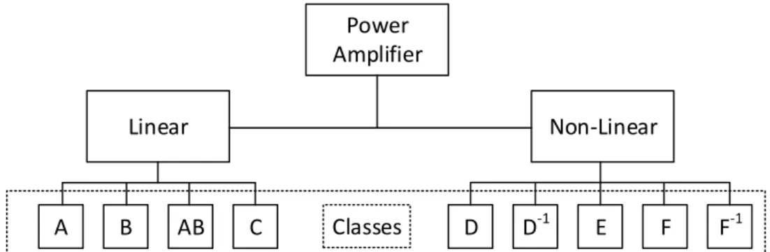
PA can also be defined by their operation mode, and can be separated in two major groups that work in linear and non-linear mode as it is shown in 2.1. The latter refers to a PA that only has phase linearity but no amplitude linearity. Amplitude linearity exists when there is a linear correlation between the output magnitude and the input voltage.
Power Amplifier
Linear Non-Linear
Classes
A B AB C D D-1 E F F-1
Figure 2.1: Power amplifiers groups and classes.
The inherent high efficiency of non-linear amplifiers is the main motivation for their wide usage. Several wireless systems and standards use only phase modulation and the corresponding waveforms do not have amplitude variations. As a consequence, the PA only needs to have phase linearity and the amplitude linearity is of no concern. Hence, the non-linear behaviour is not considered as a major drawback.
2.1.1 Linear Amplifiers
As it is seen from figure 2.1 the following classic topologies for linear power amplifiers are defined: A, AB and C. As mentioned before, this group of amplifiers is able to amplify signals with non-constant envelope, such as modulated amplitude signals. All these classes share a common topology. All of them can be implemented using the same circuit, which is depicted in figure 2.2. The amplifier class of operation is distinguished exclusively by the bias conditions. All these classes are driven with a sinusoidal waveform or approximately sinusoidal. The transistor behaves as a voltage-controlled current-source, at least for a certain portion of the wave cycle [3].
The tuned parallel LC filter, shown in figure 2.2, is not a part of the basic schematic circuit for this kind of amplifiers, even so it’s recommended to filter the signal outside the fundamental frequency. This will ensure an improvement in the efficiency of the amplifier, because the device only affects the load at the fundamental frequency. At all the other frequencies the filter acts as a short-circuit to the ground.
2.1. RF POWER AMPLIFIERS
VDC
VIN
RL
Matching Network
Cf Lf
RFC
Figure 2.2: Linear power amplifiers schematic
Table 2.1: Transistor conduction angle.
Class Conduction Angle (degrees) A 360◦(100%)
B 180◦(50%)
AB 180◦>and <360◦
C <180◦
Class-A amplifier
For the amplifier to operate as a Class-A, the bias levels must be chosen so that the transistor is kept in the active region for all the time. Hence, the drain current waveform has a conduction angle of 360◦, which is all of the wave period as shown in figure 2.3.
The Class-A has the highest conduction angle of all linear amplifiers, leading to the lowest efficiency achieved of all linear amplifiers. The maximum theoretical efficiency achieved by the Class-A is 25%, it can be calculated as,
ηD = Pout
PDC, (2.1)
= 1
2
Vout VDC
2
, (2.2)
whereVoutis the output voltage amplitude.
Hence, it can be concluded that the amplifier only achieves its 50% of maximum efficiency, when the maximal output swing occurs (Vout=VDC). If this amplifier is used
CHAPTER 2. RF POWER AMPLIFIERS OVERVIEW
[rad]
0 π 2π 3π 4π
i DS
0 I
DC
I
peak
Figure 2.3: Class-A amplifier drain current waveform for two periods.
Class-B amplifier
The Class-B amplifiers have their bias levels chosen in a way that the drain current waveform has a conduction angle of 180◦. The operation point of the transistor is located
exactly at the boundary between the cut-off and the active region [p. 117][4]. The lower conduction angle compared with Class-A lead to an increase in efficiency, but the linearity of the amplifier is degraded. The drain current waveform is depicted in figure 2.4. The Class-B drain efficiency is given by,
ηD =
π
4
Vout VDC
2
. (2.3)
[rad]
0 π 2π 3π 4π
i DS
0 I
peak
Figure 2.4: Class-B amplifier drain current waveform for two cycle.
Like in the Class-A amplifier, the maximum efficiency only occurs whenVout =VDC,
2.1. RF POWER AMPLIFIERS
signal is amplified, the average efficiency will also drop according to the envelope signal probability density function A(t).
Class-AB and C amplifiers
The Class-AB configuration works between the Class-A and Class-B operation angle, which is between 180 and 360 degrees. Depending on its bias levels, this type of amplifier conducts somewhere between 50% and 100% in each cycle. Hence, the drain efficiency lays somewhere between the 50% maximum of the Class-A amplifier or the 78.5% of the Class-B. As shown in table 2.1 the Class-C amplifier has the lowest conduction angle of all the linear amplifiers. Although the efficiency rises when the conduction angle is lowered, the amplifier becomes less linear because turning off the transistor increases the number of higher harmonics generated [p. 34][2]. This non-ideal behaviour is not considered in the present analysis. The LC resonant tank is considered to have a high-quality factor, which becomes a short circuit to undesired frequencies besides the fundamental one. The drain current waveform is presented in figure 2.5.
[rad]
0 π 2π 3π 4π
i DS
0 I
peak
Figure 2.5: Class-C amplifier drain current waveform for two cycles.
Some authors do not consider the Class-C as part of the linear amplifiers group. This is due to its low conduction angle, which greatly reduces the drain current linearity. In fact, the amplifier drain efficiency can be arbitrary increased toward 100% by decreasing the conduction angle until zero. This has the drawback of also reducing the utilization factor of the amplifier toward zero and increasing the drive power to the infinity [5]. The drain efficiency of a Class-C amplifier can be obtained by,
ηD = θ−
sin(θ)
4
sin(θ
2)−θ2cos(2θ)
, (2.4)
whereθrepresents the conduction angle [6], which for a Class-C will be between 0 and
CHAPTER 2. RF POWER AMPLIFIERS OVERVIEW
The equation 2.4 is also valid for classes A, B and AB with their respective conduction angles. Table 2.2 contains the drain efficiency of the several linear amplifiers presented. Notice that the Class-AB and C amplifiers have a range of possible values that depend on the conduction angle, as previously mentioned.
Table 2.2: Efficiency of the linear amplifiers.
Class Conduction Angle (degrees) Maximum Efficiency(η)
A 360◦(100%) 25%-50%
B 180◦(50%) 25%-78.5%
AB 180◦>and <360◦ 50% <-> 78.5%
C <180◦ 78.5% <-> 100%
2.1.2 Non-Linear Amplifiers
The non-linear amplifiers group is also known as switch-mode power amplifiers. In this group of PAs the transistors act like switches that turn on and off during operation. The classes of non-linear amplifiers are D, D-1, E, F and F-1as shown in figure 2.1. Considering
ideal switches, which don’t dissipate any power at their terminal, either the voltage is zero or the current that flows through them is zero. Thus, the resulting product voltage-current is always zero. So, the transistor dissipates no power and the efficiency must be ideally 100% [p. 541][6] if there are no other losses in the amplifier circuit. This makes this group of amplifiers a good solution to amplify constant envelope signals. The class-D is the main subject of this thesis and will be discussed in detail in chapter 3.
Class-D-1amplifier
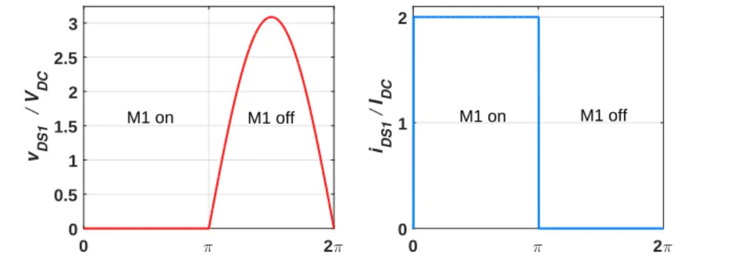
A current-mode Class-D-1amplifier topology is shown in figure 2.6. Both transistors
are driven by two square waves with opposite phase that ensures that only one transistor is active at a time. The RFCs chokes act like DC current sources, therefore, combined with the switching action of the transistor, the current always flows from one branch of the circuit to the other and passing through the RLC circuit.
The RLC parallel network is tuned for the fundamental frequency fc, for all other
frequencies it behaves like a short-circuit. Therefore, the only current flowing at RL is
the current of the fundamental frequency, which is a sinusoid, assuming that the quality factorQLof the RLC network is high enough. The sinusoidal current at the load leads to a
sinusoidal voltage at the terminals ofRL.
During the switching action of the transistors only one of them is connected at a time. When one of them is off it fells the sinusoidal voltage waveform of RLat their drain. Since
each of them is only connected for half of the period of the sine-wave voltage, the voltage felt atVDSis a half sinusoid that is shown in the figures 2.7 and 2.8.
2.1. RF POWER AMPLIFIERS VDC VIN Lf Cf RL VIN RFC RFC VDC
M1 M2
Figure 2.6: Class-D-1power amplifier schematic.
[7].
Figures 2.7 and 2.8 show the current waveform for each transistor when they are on the on-state. In this state two DC currents flow through one of the transistors connecting both RFC chokes to the ground. The transistor has to be able to withstand these two currents. A disadvantage comes from the situation when the current flows through each tran-sistor (IDS =2IDC) that leads to the conduction loss due to the internal resistance of each
transistor.
To maintain the transistor conduction loss at low levels, the internal resistance of the transistorrDS has to be smaller. This can be achieved by increasing the width of the
transistors. Hence, large transistors have to be used.
0 π 2π
v DS1 / V DC 0 0.5 1 1.5 2 2.5 3
0 π 2π
i DS1 / I DC 0 1 2
M1 on M1 off M1 on M1 off
Figure 2.7: Class-D-1transistorM
1voltage and drain current waveforms.
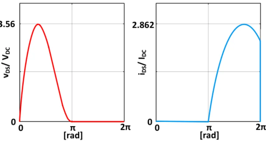
Class-E amplifier
The basic configuration of a class-E power amplifier is depicted in figure 2.9. The output network is made of series tuned circuit RLC and a shunt capacitorCs. This capacitor
CHAPTER 2. RF POWER AMPLIFIERS OVERVIEW
0 π 2π
v DS2 / V DC 0 0.5 1 1.5 2 2.5 3
0 π 2π
i DS2 / I DC 0 1 2 M2 on M2 off M2 on M2 off
Figure 2.8: Class-D-1transistorM
2voltage and drain current waveforms.
should be carefully designed, because it is responsible for the soft-switching capability of the class-E amplifier. Hard-switching devices suffer from switching losses. This occurs when the voltage across the transistor drops abruptly from a high value to zero. The shunt capacitanceCscharges and discharges between the ON and OFF state of the transistor.
Therefore, Cs does not allow instant variation in the drain voltage. This guarantees a
smooth transition between the ON-OFF states of the transistor [p. 246][4].
VDC VIN RL Cf Lf RFC CS
Figure 2.9: Class-E power amplifier schematic.
Since the class-E architecture absorbs the parasitic capacitance of the transistor with
Cs, the so-called Zero Voltage Switching (ZVS) state is achieved. This prevents energy
loss at each RF cycle, which is critical at high frequencies, thus, increasing the amplifier performance [p.53][2].
Another switch characteristic responsible for the efficiency drop in power amplifiers is the on resistanceron, associated with MOSFET transistors. This parasitic component can
be diminished by increasing the transistor size, but this also increases the parasiticCds
capacitor andCgs, increasing the driving requirements.The major drawback of the Class E
amplifier is the high drain voltage that occurs when the switch is open. This value is, in the ideal case, given byvDS ≈3.562VDC.The voltage and current drain waveforms1of the
device are presented in figure 2.10.
1The peak drain current valuei
2.1. RF POWER AMPLIFIERS
3.56
0
0 π 2π
[rad] vDS
/
VDC
2.862
0
0 π 2π
[rad] iDS
/
IDC
Figure 2.10: Class-E voltage and drain current waveforms.
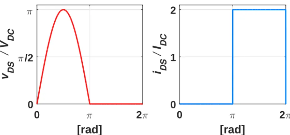
Class-F amplifier
Class-F amplifiers shown in figure 2.11, present an elegant solution in order to achieve high-efficiency. This class of amplifiers is characterized by a load network with resonance frequencies at one or more harmonic. The tank resonators are tuned to odd-harmonics, which maintain a square voltage waveform at the transistor drain and simultaneously provides a half-sinusoidal current waveform [p. 104][8]. An infinite number of tanks must be used to set the ideal waveform shaping shown in figure 2.12.
VDC
VIN
RL
Cf Lf
RFC
3fc 5fc
BFC
Figure 2.11: Class-F power amplifier schematic with 5th harmonic peaking.
Ideally, all parallel resonant circuits have infinite impedance at the corresponding harmonic resonant frequency and zero impedance at other harmonics [p. 105][8]. Conse-quently, the load impedance "felt" by the transistor isRLat fundamental frequency, infinite
at the tank resonators frequencies and zero otherwise.
CHAPTER 2. RF POWER AMPLIFIERS OVERVIEW
harmonic filtering tuned up to the 3rd or 5th harmonic only2. This lowers the obtainable
efficiency below the maximum theoretical efficiency.
[rad]
0 π 2π
v DS
/ V
DC
0 1 2
[rad]
0 π 2π
i DS
/ I
DC
0
π/2 π
Figure 2.12: Class-F voltage and drain current waveforms.
Class-F-1amplifier
The inverse class-F power amplifier can be implemented using the circuit shown in figure 2.13. The circuit shown in figure 2.12 can also be used, but now the tank resonators need to be tuned to even-harmonic resonant frequencies. This duality in the configuration can be applied also to the inverse class-F amplifier. Thereby, it is necessary, in this case, to perform the tuning only with even-harmonics [p. 161][8].
VDC
VIN
RL
Cf
Lf
RFC
3fc 5fc
Figure 2.13: Class-F-1power amplifier schematic with 5th harmonic peaking.
By analysing the schematic represented in figure 2.13 it can be seen that at the funda-mental frequency and odd-harmonics, each resonant circuit has zero impedance, but for even-harmonics they have infinite impedance. This produces the idealized square current and the half-sinusoidal voltage waveforms at the drain terminal, as shown in figure 2.14. As a result, the active device feels the load resistanceRLat the fundamental frequency,
while the odd-harmonics are shorted by the series resonant circuits [p. 161][8].
2.2. DEFINITION OF OUTPUT POWER
[rad]
0 π 2π
v
DS/ V
DC
0 π/2 π
[rad]
0 π 2π
i
DS/ I
DC
0 1 2
Figure 2.14: Class-F-1voltage and drain current waveforms.
2.2
Definition of Output Power
Figure 2.15 shows a power amplifier connected to an antenna. The output power is char-acterized by the active power delivered by the power amplifier to the antenna. In the antenna the power delivered by the amplifier is disposed under the form of electromag-netic radiation. The antenna impedanceZantennais usually designed to be entirely resistive
at the frequencies of interest. Hence, at these frequencies the antenna can be represented by a load resistorRLoad. By definition the power dissipated inRLoad is equal to the power
of the electromagnetic radiation transmitted by the antenna [Ch. 9 p. 5][9].
PA
Zantenna
VIN
PA
iout
VIN R
Load vout
Figure 2.15: Definition of power output.
In RF and microwave system it is common to designRLoad to have 50Ω. Antennas and microwave components typically have single-ended input and output impedances of 50Ω. Test equipments, as well as connector and cables used in test and modular systems,
are made with such impedance value of 50Ωthat helps in the standardization [p. 6][10]. The instantaneous output power in a given moment is defined as,
CHAPTER 2. RF POWER AMPLIFIERS OVERVIEW
The total (average) output powerPotot is given by,
Pouttot = lim
T→∞
1
T
Z T/2
−T/2po(t)dt. (2.6)
If the output voltage is a sine wave with a frequency fcand with a periodTc, the previous
equation becomes,
Pouttot =
1
Tc
Z Tc/2
−Tc/2
po(t)dt. (2.7)
Since the load is assumed to be purely resistive,
Pouttot =
1
Tc
Z Tc/2
−Tc/2
vout(t)·iout(t)dt= 1 Tc
Z Tc/2
−Tc/2
vout(t)2 RLoad dt
= V
2
outrms
RLoad . (2.8)
Where the RMS value is given by,
Voutrms =
q
v2out(t). (2.9)
One major factor is that the amplifier will not only produce power at the desired frequency, but also at the integer multiples of the fundamental frequency fc. Usually, only
the power of the fundamental frequency is desired and the harmony power has to be filtered at the output. Hence, there is only interest in the average output power of the fundamental frequency which is given by,
Pout fc =
Vout2
2RLoad
, (2.10)
whereVoutis the amplitude of the sinusoidal output voltage at the frequency fc. To obtain
this value the Fourier Series expansion ofvout(t)has to be made.
2.3
Amplifier Efficiency
The aim of the power amplifier is to deliver a certain amount of power to the load, without consuming much DC power. Figure 2.16 shows the DC power consumption of the PAPDC
which is always larger then the output powerPout.
The drain efficiencyηdis defined as,
ηd = Pout
2.3. AMPLIFIER EFFICIENCY
PA
VIN
R
Load
VDC
Pin Pout
PDC
Figure 2.16: DC power consumption
The 2.11 equation is the efficiency at the fundamental frequency since the output power
Poutis the power of the fundamental frequency defined in equation 2.10.
It can be desired to know the total conversion efficiency, which is the conversion of the total RF output power defined by equation 2.8. It includes the power of the fundamental frequency and the higher harmonics. The total conversion efficiency is given by,
ηtconv = Pouttot
PDC . (2.12)
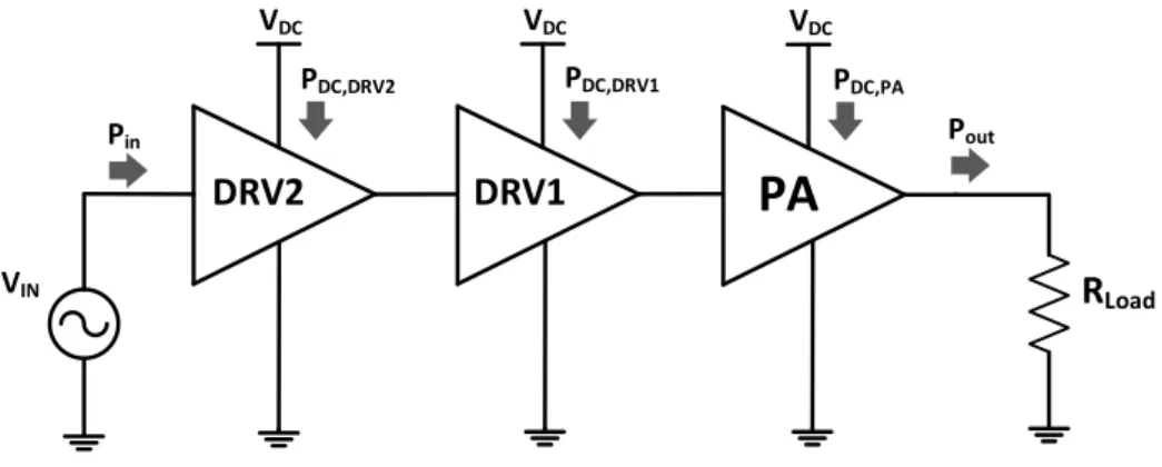
In most cases, driver stages are needed in the transmission chain as it is shown in figure 2.17. The drivers are used between the signal source and the last amplifier stage. The drivers will consume DC power, even so its not an easy task to define input and output power since the impedance levels at the input and output of each stage are different and normally composed of real and complex part.
PA
VIN
R
Load
VDC
Pin Pout
PDC,PA
VDC
DRV2
VDC
PDC,DRV2
DRV1
PDC,DRV1
Figure 2.17: DC power consumption including driver stages.
If the DC power consumption of the drivers is taken into account the overall efficiency of the PA is given by [11],
ηov= Pout
PDC,PA+∑∞i=1PDC,DRV,i
CHAPTER 2. RF POWER AMPLIFIERS OVERVIEW
The more stages the driver has, the higher power gain will be. However, it also depends on whether the amplifier is linear or non-linear. On the other hand, the amplifier overall efficiencyηovwill be degraded with the increasing number of driver stages.
If the RF input power Pin is taken into account then it leads to the Power Added
Efficiency (PAE) which is given by,
PAE= Pout−Pin PDC,PA+∑∞i=1PDC,DRV,i
. (2.14)
The drain efficiency of the PA in theory can be 100%. Yet the overall efficiency, even in the ideal case, will be less than 100%. This happens due to the power consumed in the driver stages. The power in the drivers will not reach the load, instead, it will be dissipated at the input of the next driver. Hence, even if the power amplifier and the driver stages have an efficiency of 100%, the overall efficiency will not reach such value.
So which definition of efficiency is more accurate? From the circuit point of view, the drain efficiency and the PAE seem to be more appropriate. From the system point of view, the PA is everything after the up-conversion. Hence, the overall efficiencyηovis better
suited to indicate how much power is needed to amplify the signal relatively to the output power.
2.4
Transmitter Architectures
In wireless communication systems the signal processing takes place in the digital domain at baseband frequencies, which are much lower than RF frequencies that are needed for transmission. In order for the transmission to be realized, an up-conversion from the baseband signal to RF is needed. This up-conversion can be realized with various techniques, including analogue mixing, direct digital conversion and the combination of digital/analogue up-conversion.
In a fully analogue up-conversion, the digital baseband signal is converted into an analogue signal and then up-converted into an RF analogue signal. The up-conversion can be realized in one or two steps. An RF transmitter preforms three main tasks: modulation, up-conversion and power amplification. The transmitter has three important performance specifications: modulation, spectral emissions and RF output power. In the transmitter band selection and noise are not critical parameters as in receivers, since the signal is created locally. The variations of the signal level are small, what leads to less restricted requirements in terms of the dynamic range. There are two transmitter architectures in a fully analogue up-conversion: heterodyne, that uses two step conversions from baseband to RF, and direct up-conversion, where the signal is converted directly from the baseband to RF.
2.4. TRANSMITTER ARCHITECTURES
schemes because of their influence on the choice of the building blocks of the transmitter, such as, mixers, oscillators and Power Amplifiers PA.
2.4.1 Heterodyne Transmitters
Figure 2.18 shows a block diagram of a heterodyne architecture [p. 25][12]. In the baseband two digital signals are generated,IandQ, which are converted to analog signals. During the frequency up-convention into IF, the signalQis phase-shifted by 90◦with respect to
the I signal. After the quadrature signals are summed, an IF bandpass filter is used to
remove the harmonics of the IF signal, this reduces the noise present in the signal.
PA LOHF IF 0 -90° DAC DAC DSP HF I Q LOIF
Figure 2.18: Heterodyne transmitter.
The quadrature signal I/Qis up-converted to RF and filtered again to remove the
harmonic content. The PA receives and amplifies the RF signal and sends it to the antenna to be transmitted. Due to the off-chip passive elements in IF and RF filters this architecture does not allow full integration.
2.4.2 Direct Up-conversion Transmitter
The direct up-conversion transmitter, shown in figure 2.19, converts directly the baseband signal to the RF carrier frequency, this frequency is given by the local oscillator. In this topology modulation and up-conversion occur in the same circuit. This architecture can be integrated in a better way than the heterodyne one, because there is no need for the suppression of any mirror signal generated during the up-conversion [p. 26][12]. Since the up-conversion is made in quadrature, the upper and lower sideband of the wanted signal are each others mirror signal and unwanted interference is prevented.
0 -90° DAC DAC DSP
PA
HF I Q LOHFFigure 2.19: Direct up-conversion transmitter.
CHAPTER 2. RF POWER AMPLIFIERS OVERVIEW
appear from this situation. First, the crosstalk3of the LO signal to the RF output of the
up-conversion mixer will be transmitted. Since the crosstalk effect is situated at the same frequency as the RF signal, the output bandpass filter will not be able to suppress this effect.
The second drawback is the self modulation of the local oscillator that may occur. The RF signal is up-converted and amplified by the PA to the necessary signal power to be transmitted. If the signal output power is too large it can easily couple with the sensitive local oscillator when both are at the same frequency. This effect can degrade the performance of the circuit.
2.4.3 Direct Digital Conversion
In direct digital conversion, all the signal processing and up-conversion is made in digital domain. Further, the signal is converted to the analogue domain to be amplified by the PA. The direct digital conversion architecture can be seen in figure 2.20. The baseband signal is generated with a digital modulator using a Direct Digital Frequency Synthesizer (DDFS). The signal is up-converted with an up-mixer to radio frequency. The digital RF signal is fed into D/A converter to be converted into the analogue domain to be amplified in the PA stage. The usage of a multi-bit D/A converter is susceptible to glitches and spurious noise as the RF frequency increases. The generated noise is difficult to remove by filtering the signal. The digital circuit is processing the signal in RF frequencies, leading to very high sampling frequencies causing high power dissipation[14].
PA
D/A Converter Digital
Up-mixer Digital
Modulator
Figure 2.20: Block diagram of a direct digital up-converter.
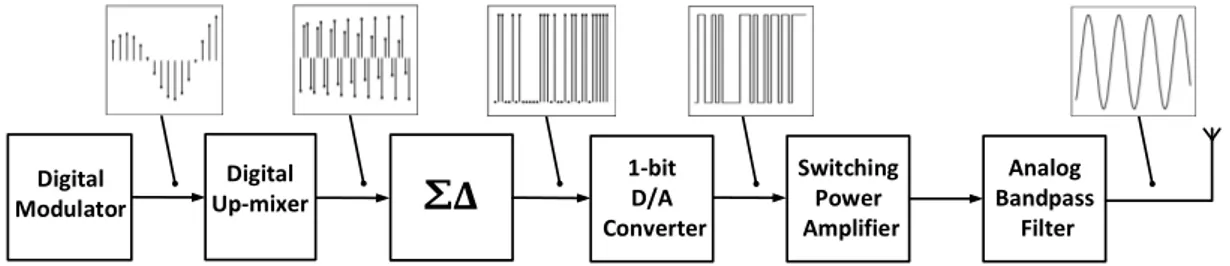
2.4.4 Sigma-Delta Direct Digital Conversion
A direct digital converter that uses a Sigma-Delta DAC4is presented in figure 2.21. This
topology is similar to the previously mentioned Direct Digital Conversion. The main difference is the replacement of the multi-bit D/A converter for a 1-bit∑ ∆D/A converter,
which solves some problems of the multi-bit D/A due to its noise shaping. But it is suitable only for relatively narrowband signal. This narrowband nature of the∑ ∆D/A
converter is suitable for many wireless communication standards, since the signal bands are relatively narrow compared to the RF carrier frequency [15].
2.5. TRANSMISSION MODULATION TECHNIQUE EXAMPLE:BLUETOOTH
The 1-bit∑ ∆DAC surpasses some of the problems related to the multi-bit DAC. Since
the output of the 1-bit∑ ∆DAC only has two levels, any mismatch of the levels results
in gain error or offset. None of these effects are of great importance in many transmitter applications. Since the∑ ∆D/A converter is a full digital circuit, it has many advantages
over analogue signal processing, such as, noise immunity, reliability, performance and power consumption that is due to the scaling of the technology. The use of a DDFS with∑ ∆D/A converter is an attractive solution for digital transmitter because it allows
the usage of switching-mode power amplifier. This implementation may lead to a high efficiency transmission [15].
1-bit D/A Converter Digital
Up-mixer Digital
Modulator
Switching Power Amplifier
Analog Bandpass
Filter
Δ
Figure 2.21: Block diagram of a direct digital up-converter using a Sigma-Delta DAC.
2.5
Transmission Modulation Technique Example:
Bluetooth
Considering the technical requirements for the PA used in this thesis, such as operating frequency, output power and the modulations schemes, the communication standard that is suited for this project is theBluetooth. It operates in the ISM 2.4 GHz frequency band,
uses low power schemes and most modulations use constant envelope signals, which can be used in switching amplifiers [p. 216][2].
The table 2.3 shows the different levels required by the Bluetooth standard [16]. It is generally used for short-distance wireless communication between several devices up to 100 meters distance.Bluetoothtechnology operates in the frequency range of 2400−2483.5 MHz including guard bands, 2 MHz wide at the bottom frequency and 3.5 MHz wide at the top frequency. TheBluetoothband is composed of 79 channels5, each channel has 1
MHz of bandwidth.
Table 2.3:BluetoothClasses.
Class (mW)Power(dBm) Range (m)
1 100 20 100
2 2.5 4 10
3 1 0 1
CHAPTER 2. RF POWER AMPLIFIERS OVERVIEW
Table 2.4:BluetoothACPR requisites.
Frequency Offset Transmit Power
±500 kHz -20 dBc
2 MHz -20 dBm 3 MHz -40 dBm
An important measurement of theBluetoothstandard is the Adjacent Channel Power
Ratio (ACPR). Most standards define ACPR measurements as the ratio of the average power in the adjacent frequency channel to the average power in the transmitted frequency channel. It describes the amount of power generated in the adjacent channel due to nonlinearities in RF components. The spectral regrowth causes interference with adjacent channels, a high spectral regrowth value can ruin the system transmission capability.
The transmitted power is measured at 100 kHz bandwidth, at maximum power. Table 2.4 shows the ACPR requirements for the Bluetoothstandard [p. 33][16]. At±500 kHz frequency offset, the transmitted power should be 20 dB below the power at zero frequency offset. In theBluetoothspecification it is denoted as -20 dBc, but it is actually 20 dB below
the power in a 100 kHz frequency band around the carrier frequency. An adjacent channel power requirement is the integrated power over 1 MHz band and it should be low enough in the neighbouring or adjacent channels. For a channel spacing of two channels, the power transmitted at 1 MHz band should be lower than -20 dBm. For a channel spacing of more than three channels, the power should be lower than -40 dBm [p. 33][16].
The firstBluetoothused Gaussian Frequency-Shift Keying (GFSK) modulation in which
the positive and negative frequency deviations represented the binary 1 and 0. With the appearance of theBluetooth2.0 + Enhanced Data Rate (EDR) the EDR brings two Phase
Shift Keying (PSK) modulation scheme. The π
4-Differential Quadrature Phase-Shift Keying
(DQPSK) and the 8-Differential Phase-Shift Keying (DPSK) can achieve speed of 2 Mb/s and 3-Mb/s, respectively, in comparison to the 1 Mb/s from the olderBluetoothversion(1.2)
[p. 34][16].
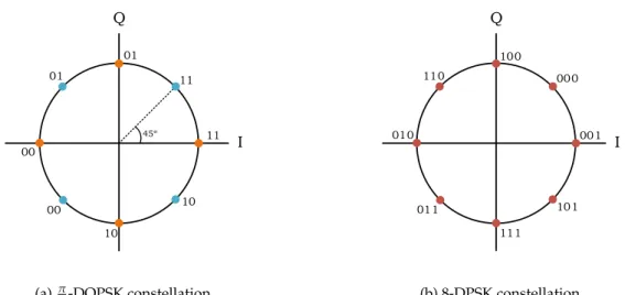
A π
4-DQPSK constellation is shown in figure 2.22a. It consists of two equal
constella-tions, 45◦(π
4) out-of-phase from each other. A jump between two symbols is always made
with3π
4 ,π4,−4π or −43π radians. Hence, the symbols are always jumping between the two
existing constellations [p. 305][17]. In figure 2.22b a 8-DPSK modulation is depicted. With this scheme it is possible to achieve the data rates up to 3 Mb/s. The utilization of 3 bits instead of 2, presented in the π
4-DQPSK modulation, ensures a higher data rate for the
2.5. TRANSMISSION MODULATION TECHNIQUE EXAMPLE:BLUETOOTH Q I 01 11 11 10 10 00 00 01 45º (a)π
4-DQPSK constellation.
Q I 100 000 001 101 111 011 010 110
(b) 8-DPSK constellation.
Figure 2.22:BluetoothModulation Schemes.
FurtherBluetoothtechnology evolved into version 3.0+HS. This evolution brings im-provements to the modulation scheme by achieving high data rate speeds comparing toBluetooth2.0 + (EDR). Even so, this version uses the non-constant envelope signals.
Therefore, a linear power amplifier should be used, whose efficiency is usually low. There are alternative solutions which use non-linear amplifiers, such as class-D with digital polar modulation[18]. However, this is outside of the scope of this thesis.
Recently a new technology, called theBluetoothV4.0+ also known asBluetoothLow
En-ergy (BLE), was developed. With the objective of providing a reduced power consumption and cost while maintaining a similar communication range comparing to classicBluetooth,
it achieves an energy efficiency 20 times higher. The extremely low peak, average and idle currents of BLE chipsets, shown in table 2.5, enable BLE devices to work with very small battery power sources for a year or more [19].
Table 2.5: BLE chipsets current consumption.
Peak Current Idle Mode Current Average Current tens ofmA tens ofnA ≈µA
BLE uses the same frequency range as Classic Bluetooth 2400−2483.5 MHz. BLE uses only 40 channels, 2 MHz wide, while Classic Bluetooth uses 79 channels, 1 MHz wide. BLE uses special channels selection techniques to save energy [19]. Also, the modulation scheme is the same: both technologies use a Gaussian Frequency Shift Keying (GFSK) modulation. BLE, however, uses a modulation index of 0.5 compared to 0.35 for Classic Bluetooth technology. This change lowers power consumption and also improves the range of BLE versus classicBluetooth[19]. The use of constant envelope signal make this
CHAPTER 2. RF POWER AMPLIFIERS OVERVIEW
Table 2.6: BLE Output Power requisites.
Minimum Output Power Maximum Output Power 0.01 mW (-20 dBm) 10 mW (+10 dBm)
C
H
A
P
T
E
R
3
RF C
LASS
-D P
OWER
A
MPLIFIER
W
ITH
S
IGMA
-D
ELTA
M
ODULATION
In this chapter a RF CDVS PA is discussed. The switching devices are MOSFET transistors. Certain conditions have to be achieved so they can operate as switches. The waveform of the Class-D will be presented and explained, it will be shown analytically that the Class-D amplifier can achieve an ideal efficiency of 100%, that is due to the Zero Current Switching (ZCS), which can be achieved in an ideal CDVS PA. A non-ideal analysis is preformed to give some insights about which factors will be involved in the degradation of the efficiency.
A MOSFET transistor, working in the linear/triode region, is presented in this chapter along with the equations that characterize it. The CMOS inverter is also described, which has two transistors working as switches, PMOS and a NMOS. The CDVS PA is analysed using and ideal and a non-ideal analysis. The CDVS PA needs to be driven due to the high capacitance present at the gate, therefore, a gate driver that solves this problem is presented in this chapter. The output series-resonant circuit is a bandpass Butterworth filter that is also presented here with the design equations.
A 1-bit Sigma-Delta∑ ∆modulator is described at the end of the chapter. It produces
CHAPTER 3. RF CLASS-D POWER AMPLIFIER WITH SIGMA-DELTA MODULATION
3.1
MOSFET as a Switch
The active devices employed in the CDVS PA are MOSFET transistors, in this case the expressions given are for NMOS transistor. It is desirable that the transistors work as switches. For this to be achieved the transistor is set to work on the triode/linear region which is given by,
VGS>Vtn,
VDS ≤Ve f f =VGS−Vtn.
(3.1)
IfVGS > Vtn, the transistor operates in the strong inversion, and ifVDS ≤ Ve f f, the
transistor is operating in the triode region. After both conditions are set, a current starts to flow trough the transistor from the drain to the source. The triode region equation for a MOSFET transistor, that relates the drain current to the gate-source and drain-source voltages, is given by,
iD =µn0CoxW
L(VGS−Vtn)VDS− VDS2
2 ). (3.2)
Where µn0 is the low-field electron mobility of the channel and Coxis the gate oxide
capacitance per unity area1. The channel resistance of a MOSFET in the ohmic region2is
as shown,
rDS = i1
D
VDS
= 1
µn0CoxWL(VGS−Vtn)−V 2 DS 2 )
, (3.3)
sinceVDS is very small, the previous expression can be simplified to
rDS ≈ 1
µn0CoxWL(VGS−Vtn)
. (3.4)
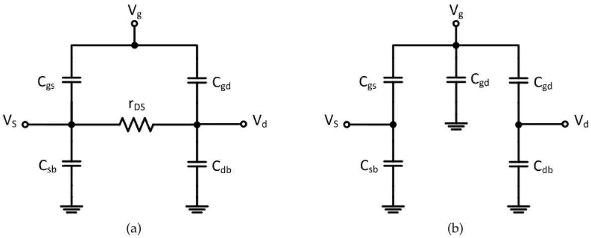
The accurate small-signal modelling of the high-frequency operation of a transistor in the triode region is non-trivial. Therefore, a simplified model is used for a smallVDS
as shown in figure 3.1a. The resistancerDSin the figure is given by (3.4). Here the gate to
channel capacitance has been evenly divided between the source and drain nodes,
Cgs= Cgd = 1
2CoxW L. (3.5)
This equation neglects overlap between the gate and source junction, which is Cov = W LovCox, where Lovis the effective overlap distance. If accuracy is very important then
this equation should be taken into account. The capacitances Csb and Cdb are highly
non-linear, their equations and explanation are quite endeavouring.3 1K
n=µn0Coxis the intrinsic transconductance of the transistor.
2Also known as Triode or Linear region, in this region the MOSFET operates like a resistor, controlled by the gate voltage relative to both the source and the drain voltage [21].
3C
3.1. MOSFET AS A SWITCH
Vg
VS
rDS
Cdb
Csb
Cgs Cgd
Vd
(a)
Vg
VS
Cdb
Csb
Cgs Cgd
Vd
Cgd
(b)
Figure 3.1: Small-signals models. (a) Simplified triode-region model for a smallVDS. (b)
MOSFET model when is turned off.
When the transistor is on the off state, the small signal model changes substantially this new model as it is shown in figure 3.1b. One of the major differences is thatrDS is
now infinite. Another difference is thatCgsandCgd are now much smaller. Since there is
no channel, these capacitors only exist due to the overlap capacitance. Hence, we have
Cgs =Cgd =W LovCox. (3.6)
The reduction of the Cgs and Cgd doesn’t mean that the total gate capacitance will
be smaller. This model contemplates a new capacitorCgb, which is the gate to substrate
capacitance and is given byCgb=W LCox. The capacitancesCsb andCdbare not taken into
account for reasons stated above.
Making a quick review, for the MOSFET to behave like a switch, the following con-ditions have to be achievedVGS > Vtn,VDS ≤ Ve f f. If the first condition isn’t achieved,
the transistor will behave like an open switch4, no current will be able to flow through.
After the first condition is met, the second one will ensure that the transistor will be on the triode region. In the triode region the MOSFET will behave like a closed switch with a small resistance(rDS), and current is able to pass. In the other hand the gate capacitances Cgs,Cgdwill require a driver before the Class-D PA, this issue will be discussed further
ahead.
4The resistancer
CHAPTER 3. RF CLASS-D POWER AMPLIFIER WITH SIGMA-DELTA MODULATION
3.2
CMOS Inverter
The main building block of the CDVS PA (figure 3.4) is the CMOS inverter (figure 3.2), which is used in digital circuit design. This block is the PA and it is responsible for converting DC power into RF power. The MOSFET transistors PMOS (Mp) and NMOS
(Mn) work as switches. When the input of the inverter is connected to the ground(VI N =0), the output is connected directly toVDCthought the PMOS transistorMp.
When at the inputVI N = VDC, the output is connected toGNDthought the NMOS
transistorMn. With the switching action at the output of the CMOS inverter the voltage
swings between the DC supply voltageVDCand the ground. The switching threshold
can be set to different values by changing the device size (width), that will also affect the output voltage-swing. Another important fact is that the static power dissipation in the CMOS inverter is practically zero.
VDC
MN MP
VIN VOUT
-+ + -VSGp VGSnFigure 3.2: CMOS inverter schematic. A Ouput Voltage (V) Input Voltage (V)
1 2 3
Mp On Mn Off
Mp Off Mn On Both on Vout_H Vout_L Vin Vin B L H
Figure 3.3: CMOS inverter transfers characteristics.
The inverter from the figure 3.2 has the transfer characteristics shown in figure 3.3. When the input voltage is low enoughVI N < Vin
L, the inverter is in the region 1. Here
VSGp>Vth5, the transistor Mnis off andMpis on, and the output voltage becomesVout H.
WhenVI N >Vin
H, the inverter is in the region 3. HereVGSn >Vth,Mnis on,Mpis off and
the output voltage isVoutL.
In region 2, ifVinH > Vin > VinL then both transistors Mn andMpare on. Therefore,
the current flows fromVDCto the ground and, thus, power is lost during this transition.
This is the main loss mechanism in the CMOS inverter also known as dynamic power loss.
5V
3.3. CLASS D VOLTAGE-SWITCHING POWER AMPLIFIER
3.3
Class D Voltage-Switching Power Amplifier
A CDVS PA circuit is shown in figure 3.4, where the switching devices are a PMOS (Mp) and a NMOS (Mn) transistors. Such configuration is known as an inverter device
which is shown in figure 3.2. This topology requires only one driver, however, the cross conduction of both transistors during the MOSFETs transitions may cause spikes in the drain currents. Solutions can be found to avoid this problem, but they are used for low frequency applications, and at RF frequencies the driver complexity increases considerably [23].
VDC
MN
MP
VIN
L C
R vO
Figure 3.4: A CMOS CDVS PA with a series-resonant circuit.
The peak-to-peak value of the gate-to-source driver voltageVI N is equal or close to the
DC supply voltageVDC. This circuit is appropriate only for low values ofVDC. For high
values of VDC,VI N will be high as well, this may cause voltage breakdown of the gate
oxide. The oxide breakdown is a very harmful effect, since it limits the maximum signal swing on the transistor drain. This is one of the main issues of designing PA in sub-micron CMOS technology.
Another issue is the hot carrier effect, it reduces the reliability of the transistor by in-creasing the threshold voltage, and consequently the performance is degraded. A detailed explanation of this effect can be found in [p. 56][2].
3.3.1 Ideal Analysis
The analysis of the circuit from figure 3.4 will be explained. The following considerations have to be made for this analysis:
• The on-resistancerDSand the parasitic capacitances of the transistor are neglected,
and the switching between on and off state is instantaneous.
• The elements of the series-resonant circuit are passive,linear, time invariant, without
CHAPTER 3. RF CLASS-D POWER AMPLIFIER WITH SIGMA-DELTA MODULATION
• The quality factor of the series-resonant is high enough so that the current through
the load resistanceRis sinusoidal.
• The total resistance of the circuitRtwill only take into account the load resistanceR.
VSGp
π 2π ωt VGSn ωt VSDp ωt VDC VDSn ωt i ωt Im ωt iMp IDC ωt Im iMn Im MP_on MN_off MP_off MN_on
Figure 3.5: Waveforms of a CDVS PA.
The waveforms of a CDVS PA are illustrated in figure. 3.5. The influence of the input signalVI Ncan be seen here.
When VI N = 0 the source-gate voltage of the PMOS is
VSGp = VDC and the transistor Mp is turned on, while Mnis off. Since the transistor is considered ideal it has no internal resistance, the drain-source voltage is VSDp = 0
whileVDSn =VDC. Subsequently, a currentiMp flows from
VDCthroughMp, the series-resonant circuit and the load
resistance R. Due to the high quality factor of the
series-resonant circuit the current sensed by the resistanceRis a
positive half-sinusoid with amplitudeImwhenMpis on .
On the opposite side, whenVI N = VDCthe gate-source
voltage of the NMOS isVGSn=VDCand the transistorMn
is turned on, while Mp is off. Consequently,VSDp = VDC
andVDSn =0. A currentiMn, flows from the load resistance
Rthrough the series-resonant circuit,Mnand to the ground.
Since the current flows on the opposite side of how the voltage is felt atRthe currentiis a negative half-sinusoid
with amplitudeIm.
One question can be raised here. When Mnis on and Mpis off, the current flows fromRtoMn, and a closed loop
is created connecting both ends to the ground, no power supply is present. So how can current flow in the circuit? The reason for this to happen is the series-resonant circuit, which is an LC series filter, composed of an inductor and a capacitor. The inductor has the capacity of storing energy in its magnetic field when current is flowing, and the capacitor also has the habitability to store charge in its electrical field.
When power is drained fromVDCto the load, current
flows to the circuit and energy is stored in the inductor’s
magnetic field. After the switches commute,Mnis turned on andMpis off. At this time the currentiMnstarts to flow from the drain to the source. Consequently, the energy stored
in the inductor starts to be channelled in the direction ofMnto the ground.
As stated above the series-resonant circuit is an LC filter and has the function of filtering the fundamental frequency present in the signalVI N, delivering it to the load resistanceR.
The filter has to be tuned for the fundamental frequency ofVI N. This frequency is called
3.3. CLASS D VOLTAGE-SWITCHING POWER AMPLIFIER
In figure 3.5 it is noticeable that the voltage waveforms at the transistors’ terminals
VDS don’t overlap with the current waveforms, thus, no power is dissipated. When the
transistor switches from one state to the other the current at their terminal is 0, so we can say that the ZCS is achieved.
The transistors are considered to be ideal, therefore, with the switching action at their terminals a square-wave is produced with the same frequency ofVI N. So the input voltage
at the series-resonant circuit is a square wave (v)
v≈VDSn =
VDC for 0<wt≤π,
0 forπ <wt≤2π.
(3.7)
This voltage can be expressed by the trigonometric Fourier series
v≈VDSn =VDC
" 1 2 + 2 π ∞
∑
n=1
1−(−1)n
2n sin(nwt)
#
=VDC
( 1 2 + 2 π ∞
∑
k=1
sin[(2k−1)wt])
2k−1
)
=VDC
1
2+ 2
πsin(wt) +
2
3πsin(3wt) +
2
5πsin(5wt) +...
. (3.8)
Ideally, the even harmonics (n= 2, 4, 6,· · ·) in a square-wave signal are zero.
For frequencies lower than the resonant frequency f0, the series-resonant circuit
rep-resents a high capacitive impedance. On the other hand, for frequencies higher than the resonant-frequency f0, the series-resonant circuit represents a high inductive impedance.
The series-resonant circuit acts as a bandpass filter. If the load quality factorQLis high
enough, the voltage across the resistance R at f = f0is only the fundamental component
present in (3.8),
v=Vmsin(wt), (3.9)
where its amplitude is given by,
Vm = 2
πVDC. (3.10)
And the current through the resonant circuit at f = f0is approximately sinusoidal and
equal to,
i= Imsin(wt), (3.11)
where
Im = Vm Rt =
2VDC
CHAPTER 3. RF CLASS-D POWER AMPLIFIER WITH SIGMA-DELTA MODULATION
At the resonant-frequency f = f0, the currentiDCdrawn from the DC power supply is
equal to the current that flows through the upper transistorMpand is given by,
i1=iMp =
Imsin(wt) for 0<wt≤π,
0 forπ <wt≤2π.
(3.13)
The DC component of the supply current is,
IDC = 1
2π Z 2π
0 iMpdwt=
Im
2π Z π
0 sin(wt)dwt=
Im
π =
Vm
πRt. (3.14)
From 3.12 and 3.14, the power requested from the DC power supply is,
PDC=VDCIDC = 2V
2
DC
π2Rt. (3.15)
And, the power delivered to the output is,
PO= RI
2
m
2 =
2VDC2 R
π2R2t . (3.16)
The drain efficiency of the Class-D with ideal transistor (rDS =0, and with instanta-neous switching time) is,
ηD = PO
PDC =1. (3.17)
Therefore, the ideal efficiency of the Class-D voltage-switching PA is 100%.
3.3.2 Non-Ideal Analysis
A more accurate analysis of the real efficiency of the Class-D PA will be presented in this section. The expressions presented here do not describe the real system, but instead provides a more realistic approach to understand which factors will degrade the efficiency of the amplifier. For the non-ideal analysis we assume that:
• The transistor has an on-resistancerDSwhich is linear. It is assumed that the
resis-tance of both PMOS and CMOS transistors is the samerDS =rDSp =rDSn.
• The transistors’ parasitic capacitances are considered to be linear.
• The elements of the series-resonant circuit are passive,linear, time invariant and
without parasitic reactive components.
• The inductor in the series-resonant circuit has an internal resistancerL.