ScienceDirect
Physics Procedia (2014) 000–000
www.elsevier.com/locate/procedia
1875-3892 © 2014 The Authors. Published by Elsevier B.V.
Peer-review under responsibility of the organizing committee of ICEC 25-ICMC 2014.
25th International Cryogenic Engineering Conference and the International Cryogenic Materials
Conference in 2014, ICEC 25–ICMC 2014
Building a thinner gap in a Gas Gap Heat Switch
J. Franco, B. Galinhas, P. Borges de Sousa, D. Martins, I. Catarino, G. Bonfait
CEFITEC, Departamento de Física, Faculdade de Ciências e Tecnologia - Universidade Nova de Lisboa, 2829-516 Caparica, Portugal
Abstract
A gas gap heat switch (GGHS) reaches its highest conductance state when the gap between two exchange surfaces is filled with a conducting gas in a viscous regime. The broader the surface and the thinner the gap, the higher the ON conductance achieved. In this paper we describe a very thin cold gas gap heat switch reached upon the use of the differential thermal expansion of the construction materials. Such technique overcomes the intricacies of the manufacturing process of the switch.
We designed built and tested a prototype of a very thin gap heat switch using our new methodology. The high conductance was measured with both helium and nitrogen, at temperatures ranging from 20 K (He) or 75 K (N2) up to room temperature. The inferred gap opening at low temperature (≈ 17 µm) has shown to be slightly above the expected, which allowed us to reinterpret the design calculations. The switch was also characterized along its extreme conductance states while using a sorption pump, and its performance was compared with a previously developed model.
Lessons learned from the first prototype led us to build a second one with better performance.
Our experiments suggest that the proposed design allows for the development of a customized cryogenic switch with improved ON conductance while keeping the assembly very simple and sturdy, hence widening the scope of applicability of these devices.
© 2014 The Authors. Published by Elsevier B.V.
Peer-review under responsibility of the organizing committee of ICEC 25-ICMC 2014.
Keywords: gas-gap heat switch; DTE
1.
Introduction
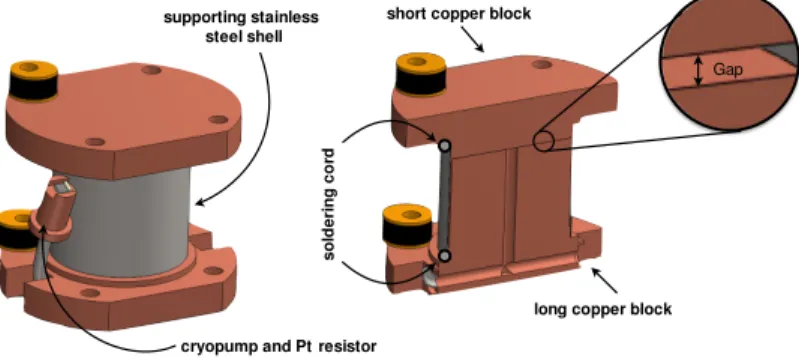
Fig. 1. (a) The switch prototype as designed and built: the inner copper blocks contracting by cooling down more than the outer stainless steel supporting shell leads to a narrow gap opening between the blocks; (b) the cut evidences the gap as well as the soldering cord.
In such type of switch, the ON state is obtained by introducing a gas between two copper blocks separated by a very narrow gap — typically 100-200 microns — to obtain a good conductance through the gas. Despite the rather low thermal conductivity of a gas, the narrower the gap the best the conductance. The OFF state is obtained by removing the gas, for instance by using a small cryopump. Heating or cooling the cryopump allows toggling between the ON and the OFF conduction states of the switch, achieved in the absence of any moving parts. The two copper blocks are held apart by a thin stainless steel tube (typically 100-200 m thick) to avoid short-circuiting the blocks as well as to enclose the working gas.
Our laboratory built some of these switches for management of energy storage units [2,3] and keeps working on this topic for other applications. As previously explained, the gap thickness is fundamental to obtain a high conductance in the ON state and is generally obtained thanks to quite precise machining and alignment during mounting and welding, in order to avoid a misalignment that would lead to thermal contact between the copper blocks.
Fig. 2. The gap opening between both copper blocks of the switch, as a function of temperature. The black solid line computes the gap opening, as the switch was considered isothermal during the soldering process and with 15 mm between the soldering cords. In such an isothermal soldering the expected gap is null at 221ºC (melting temperature of the solder), being ≈ 4 µm at room temperature and 8 µm below 70 K. The
green solid line depicts the gap opening for a room temperature fixture of the pieces. The dashed line represents the variation of the gap opening assuming that the stainless steel support was 35 ºC colder that the copper blocks at the soldering process and matches the experimental results.
In a recent article [4] we proposed and tested a switch in which the gap was obtained using the differential thermal expansion of copper and stainless steel (SS): If two simple copper cylinders are in contact at room temperature and kept face-to-face with a SS support enclosing the working gas (figure 1), during cooldown, the
Gap
long copper block short copper block
s
o
ld
e
ri
n
g
c
o
rd
cryopump and Pt resistor supporting stainless
copper blocks (α 1.65x10⁻⁵ K-1 at RT) will contract more than the SS support (α 1.54×10⁻⁵ K-1 at RT) and a gap between the two copper blocks will naturally grow. In the tested switches, the total length of the copper blocks was 15 mm leading to a gap of 3.7 m at 70 K. Below this temperature, both copper and SS stop to contract and the gap will remain the same down to lower temperature: a gap of 4 m could be obtained without complicated machining and alignment process! In the following, we will revisit the problems that occurred in this first version of such a switch and how we tried to solve it.
2.
First version (V0) of the dilation heat switch (all soldered)
The first dilatation heat switch was designed as previously described and the SS support was soldered using a low temperature solder (Ag-Sn, melting point 221ºC). Actually, in such a process, the two copper blocks (diameter 21.4 mm, 15 mm total length of the two blocks) are in contact at this temperature and when the solder solidifies the gap starts to grow (black line in figure 2) leading to a gap of 4 µm at 300 K and 8 µm at 70 K.
The ON state of the built prototype was characterized with helium and nitrogen for various pressures, kept constant along the temperature range. The results of figure 3-a (nitrogen gas) show that the ON conductance is pressure independent, indicating that the viscous regime is well established for these 3 pressures. As is also shown in figures 3-a and 3-b, the results are only well described considering a gap around 13 m at 300K (blue line). Such a larger gap, compared to the expected one, can be explained supposing that during the soldering phase the main part of the SS support is colder than the copper blocks: such a thermal gradient can exist due to the poor conduction and low thermal capacity of this SS thin tube. In such a condition, this support will contract less during the cooling at RT: this smaller contraction leads to a larger gap at room temperature. This 13 m gap at 300 K would be explained by a mean temperature of the support 35ºC lower than that reached by the copper blocks ( 221ºC) during the soldering process. As this explanation seemed quite plausible, we decided to substitute this last soldering step by a gluing process in order to obtain a null gap at room temperature. More information on this first version switch can be obtained in [4].
Fig. 3. (a) Nitrogen; (b) Helium (adapted from [4]): The symbols represent the experimental results in the ON state for the switch conductance determined with a 2 W heating power. The green line represents the calculated switch conductance with the hypothesis of a null gap at 300 K, the
blue line with the hypothesis of a gap equal to 13 µm at 300 K.
3.
Second and Third versions (V1 and V2) of dilatation heat switch (soldered and glued)
The second prototype (V1) was then tested and the variation of its thermal resistance versus the temperature, displayed in figure 4 (squares), was obtained with helium gas, applying 1 W to the short block and under a constant pressure of 360 mbar. (This pressure insures a viscous regime as verified a posteriori by doing same measurements — not shown — at higher pressure). A careful analysis was performed again in order to obtain a precise gap measurement. In figure 4 the contributions of helium and copper thermal resistances are displayed: the final thermal resistance is the sum of both contributions. The thick grey line represents the thermal resistance of the copper blocks using the RRR50 copper thermal resistivity (ETP Copper). The short-dashed line depicts the thermal resistance of helium gas in the gap when assuming it to be null at 300 K. The thin solid line shows the sum of the latter two contributions. It is clear that that this line does not fit the experimental results. Once the copper contribution becomes quite small, when compared to the gas one, for temperatures below 50 K, this unsatisfactory fitting cannot be due to the copper contribution but only due to an error of the gap estimate. Taking the gap size as an adjustable parameter, a gap equal to 11 m can fit quite well the results (thick solid line), the gas thermal resistance with an 11 m gap being represented by the long dashed line. Being very difficult to explain such a large gap due to thermal reasons, its origin could be explained by some existing dust between the two copper blocks or by a high roughness or imperfect surface state of the two copper block faces. As a matter of fact, if one defect on the two blocks surface leads to 11 m separation at 300K, the null gap will never be obtained. Let us note that these local contacts will not significantly decrease the thermal resistance.
Then a third heat switch was built with special care concerning the surface finishing. In particular, the two faces of the copper blocks were polished and the result was measured on selected spots of the surfaces by a surface roughness meter along 4 mm: a maximum roughness of 1 µ m was measured. The switch was mounted and tested and its results (circles in figure 4) were not all better than the previous version! These very similar results seem to indicate that the global roughness of the two faces is not the predominant cause for the 11 µm gap at room temperature. Other more or less singular surface defects appearing during the mounting process could be invoked. Another hypothesis could be assigned to a lack of rigor in the design/machining of the parts that leads to a defective mounting of the two copper blocks such that they are never in face contact. Despite critical analysis of the drawings as well as rigorous inspection of the manufactured pieces were performed, we cannot totally exclude such an explanation.
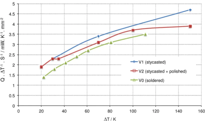
Because version 0 and versions 1 and 2 have different surface areas on the copper blocks, the conductances of the V0 (soldered) and V1 and V2 (stycasted) prototypes are normalized, calculating the conductance by unit area (Figure 5). This plot shows that the “stycasted” switches are more efficient than the soldered one by 20%. The gap at 300 K is indeed slightly smaller in the “stycasted” versions, but even so it is not zero.
Fig. 5. Normalized conductance results (per exchange surface area) for the three versions of the built switches.
4.
Concluding remarks
The version V0 of this type of dilatation switch showed that a gas gap heat switch with reasonable performances can be built very simply and the ON conductance state can be compared with other types of gas gap heat switches [1-3]. Unfortunately, in versions V1 and V2, we did not succeed in obtaining a gap smaller than 11 m at 300 K. As shown by the thin continuous line of figure 4, if a null gap (green line) at room temperature could be obtained, the thermal resistance could be reduced by a factor of ~ 4. It could be possible but it seems that, in order to obtain this high ON conductance, the simplicity of construction that initially motivated this work would disappear. Let us also note that, if the application of the switch is not very demanding about the OFF state — as the resistance of this OFF state decreases with decreasing the switch length — a very compact heat switch can be obtained using this method.
References
[1] I. Catarino, G. Bonfait, L Duband, Neon Gas-Gap Heat Switch, Cryogenics. 48 (2008) 17–25.
[2] G. Bonfait, I. Catarino, J. Afonso, D. Martins, M. Linder, L. Duband, 20 K Energy Storage Unit, Cryogenics. 49 (2009) 326–333. [3] I. Catarino, J. Afonso, D. Martins, M. Linder, L. Duband, G. Bonfait, 6 K solid state Energy Storage Unit, Cryogenics. 50 (2010) 102–110. [4] J. Franco, D. Martins, I. Catarino, G. Bonfait, Narrow gas gap in cryogenic heat switch, Applied Thermal Engineering. 70 (2014) 115–121.
Acknowledgements
This work was partially supported by Fundação para a Ciência e Tecnologia (PTDC/EME-MFE/101448/2008, PEst-OE/FIS/UI0068/2014 and PTDC/EMS-PRO/1065/2012). JF, DM and PBS acknowledge the Fundação para a Ciência e Tecnologia for their fellowships.
0 0.5 1 1.5 2 2.5 3 3.5 4 4.5 5
0 20 40 60 80 100 120 140 160
Q
.
T
-1 .
S
-1 /
m
W
.
K
-1.
m
m
-2
T / K
V1 (stycasted)
V2 (stycasted + polished)
![Fig. 3. (a) Nitrogen; (b) Helium (adapted from [4]): The symbols represent the experimental results in the ON state for the switch conductance determined with a 2 W heating power](https://thumb-eu.123doks.com/thumbv2/123dok_br/16543641.736843/3.892.102.792.571.813/nitrogen-helium-adapted-symbols-represent-experimental-conductance-determined.webp)