Rodrigo Cortes dos Santos
Licenciado em Engenharia de Micro e Nanotecnologias
Copper nanowires for next generation
transparent conductors
Dissertação para obtenção do Grau de Mestre em
Engenharia de Micro e Nanotecnologias
Orientador:
Doutor Pedro Miguel Cândido Barquinha, Professor Auxiliar,
Faculdade de Ciências e Tecnologia da Universidade Nova de Lisboa
Júri:
Presidente: Doutor Rodrigo Ferrão de Paiva Martins, Professor Catedrático, Faculdade de Ciências e Tecnologia da Universidade Nova de Lisboa
Arguente: Doutor Rui Alberto Garção Barreira do Nascimento Igreja, Professor Auxiliar, Faculdade de Ciências e Tecnologia da Universidade Nova de Lisboa
Vogal: Doutor Pedro Miguel Cândido Barquinha, Professor Auxiliar, Faculdade de Ciências e Tecnologia da Universidade Nova de Lisboa
Copper nanowires for next generation transparent
conductors
Copyright © Rodrigo Santos,
Faculdade de Ciências e Tecnologia,
Universidade Nova de Lisboa.
i
ACKNOWLEDGMENTS
First of all, thanks to professor Rodrigo Martins for the assembly of this breakthrough master degree, and professor Elvira Fortunato for allowing me to do research in this excellence center, which is CENIMAT.
A big thanks to professor Pedro Barquinha for your orientation, advices, meetings, and also for the opportunity of exploring a new branch of conductor films.
To Daniela Gomes for all your help, SEM images and advices, and to Ana Rovisco for guiding the newbie around the lab, SEM images, materials, advices, and patience.
To Lídia Santos and Rita Branquinho, who attended “Synthesis and integration of oxide
nanostructures’ group” and gave a lot of useful advices and help.
To the “lab 2’s mothers”, Alexandra Gonçalves, and Sónia Pereira. You two had a lot of patience and always supplied me everything that I needed.
To Dona Antónia for bringing the Portuguese newspaper “Público” to CENIMAT, making my
waiting till the reaction’s end much more tolerable.
To Ismael Domingos, my partner in the lab and in the nanowires research.
To Rui Carreiras, Pedro Freitas and the “coach” José Correia, also known as the “team”, for all the nice matches, and some not so nice…
To my friends, who supported me throughout this roller coaster, especially Ana Figueiredo. To Andreia dos Santos, a singer, pianist, poetess and writer. As I mentioned, you are the one good with words, so I cannot verbalize how thankful I am.
iii
ABSTRACT
In this work, copper nanowires (CuNWs) were synthesized for application in transparent conductors, as an exploratory work for the replacement of conventional indium-tin oxide (ITO) thin films. Two syntheses were made, one of them costing less than 4 € per synthesis. Numerous deposition methods were applied and several nanowire inks were used. The best ink was shown to be CuNWs with 7 wt% in isopropyl alcohol (IPA), and a newly developed method was designed to deposit NWs.
The ink of CuNWs was deposited on top of interdigitated electrodes on glass. CuNWs on electrodes with gaps of 5, 10 and 30 µm registered a resistance as low as 68.07, 25.81 and 71.84 Ω,
respectively. The films deposited directly on glass with top electrodes revealed a high electrical resistance, presumably due to high contact resistance. Inefficient intra-network welding (i.e., between NWs) was also responsible for the trend of increased resistance with higher number of consecutive depositions. Manual pressing was applied to the films, however, this process peeled off some CuNWs due to the lack of surface adhesion. So, numerous surface treatments were applied to glass surfaces, but then the surface roughness did not allow for a perfect deposition of aluminium contacts by e-beam. The optical properties of the films with different thicknesses (obtained with several subsequent depositions) were measured, with the optical transmittance decreasing for larger number of depositions. Best equilibrium in terms of electrical/optical properties was achieved with a single deposition, for which electrical resistance of 65 Ω (5 µm gap) and 90 % optical transmittance were obtained.
v
RESUMO
Neste trabalho sintetizaram-se nanofios de cobre (CuNWs) para aplicar em condutores transparentes, como um trabalho exploratório para substituição de filmes convencionais de óxido de índio-estanho (ITO). Foram feitas duas sínteses, sendo que uma custa menos de 4 € por síntese.
Testaram-se inúmeros métodos de deposição e utilizaram-se várias tintas de nanofios. Demonstrou-se que a melhor tinta consistia em CuNWs com 7 % (m/m) em álcool isopropílico (IPA), e um novo método de deposição de NWs foi desenvolvido.
A tinta de CuNWs foi depositada no topo de elétrodos interdigitais em vidro. Os CuNWs em elétrodos com espaçamentos de 5, 10 e 30 µm registaram resistências de 68.07, 25.81 e 71.84 Ω, respetivamente. Os filmes depositados diretamente no vidro revelaram uma elevada resistência elétrica, presumivelmente devido à elevada resistência de contacto. Uma ineficaz soldadura intra-rede (i.e, entre NWs) foi responsável pelo aumento da resistência com o incremento do número de deposições. Aplicou-se pressão manual nos filmes, contudo, este processo arrancou alguns CuNWs devido à sua baixa adesão à superfície. Por este motivo, aplicaram-se vários tratamentos de superfície aos substratos de vidro, no entanto a rugosidade não permitiu uma deposição perfeita de contactos de alumínio por canhão de eletrões.
Mediram-se as propriedades óticas dos filmes com diferentes espessuras (obtidas através de várias deposições), com a transmitância ótica a diminuir com o aumento do número de deposições. O melhor equilíbrio em termos de propriedades elétricas/óticas foi alcançado com uma única deposição, com a qual se conseguiu uma resistência elétrica de 65 Ω (5 µm de espaçamento) e uma transmitância ótica de 90 %.
vii
LIST OF ABBREVIATIONS
a.u. – Arbitrary units
AgNW – Silver nanowire
APTES – (3-Aminopropyl)triethoxysilane
CENIMAT – Centro de investigação de materiais
CNT – Carbon nanotube
Cu – Copper
CuNW – Copper nanowire
EDA – Ethylenediamine
EtOH – Ethanol
FIB – Focused ion beam
IPA – Isopropyl alcohol
ITO – Indium tin oxide
LED – Light emitting diode
Mw – Molecular weight
NaOH – Sodium hydroxide
NW – Nanowire
OLED – Organic light emitting diode
OPV – Organic photovoltaic
PEDOT:PSS – Poly(3,4-ethylenedioxythiophene):polystyrene sulfonate
PV – Photovoltaic
PVP – Polyvinylpyrrolidone
rpm – Rotations per minute
SEM – Scanning electron microscope
UV – Ultraviolet
ix
LIST OF SYMBOLS
R – Electrical resistance
xi
TABLE OF CONTENTS
ACKNOWLEDGMENTS ... I
ABSTRACT ... III
RESUMO ... V
LIST OF ABBREVIATIONS ... VII
LIST OF SYMBOLS ... IX
TABLE OF CONTENTS ... XI
LIST OF FIGURES ... XIII
LIST OF TABLES ...XV
1. MOTIVATION AND OBJECTIVES... 1
1.1. Motivation ... 1
1.2. Objectives ... 1
2. INTRODUCTION ... 3
2.2. Copper and copper nanowires ... 4
2.3. Synthesis of copper nanowires ... 4
2.4. Fabrication of copper nanowires films ... 5
2.5. Reduction of the contact resistance between copper nanowires ... 6
2.6. Protection from oxidation ... 6
2.7. Highly stretchable and foldable electrodes ... 7
2.8. Device Integration ... 7
3. MATERIALS AND METHODS ... 9
3.1. Copper nanowires synthesis ... 9
3.1.1.Synthesis using copper acetate ... 9
3.1.2.Synthesis using copper nitrate ... 9
3.1.3.Materials and reagents ... 10
3.1.4.Cleaning and dispersion of the nanowires ... 10
3.1.5.Characterization of copper nanowires: morphological and structural analysis ... 10
3.2. Copper nanowires films ... 10
3.2.1.Materials and reagents ... 10
3.2.2.Characterization of copper films: morphological, electrical and optical analysis ... 11
xii
4. RESULTS AND DISCUSSION ... 13
4.1. Copper nanowires synthesis ... 13
4.1.1.Synthesis using copper acetate ... 13
4.1.2.Synthesis using copper nitrate ... 15
4.2. Deposition methods ... 17
4.2.1.Drop Casting ... 17
4.2.2.Spray coating ... 19
4.2.3.Doctor blade ... 19
4.2.3.1. Electrical characterization………...……….. 21
4.2.3.1. Nanowires on interdigitated contacts ……….. 22
4.2.3.1.2 Conductive copper nanowires films ……….. 25
4.2.3.2.Optical characterization ………. 28
5. CONCLUSIONS AND FUTURE PERSPECTIVES ... 29
5.1. Final conclusions ... 29
5.2. Future perspectives ... 30
6. BIBLIOGRAPHY ... 31
xiii
LIST OF FIGURES
Figure 2.1 – Graphic showing some of the results obtained so far by other research groups. In Chang et al. [20] the average values were considered. Shi et al. [21] did not fully specify the CuNWs length and the diameter was an average of the results presented. Zhang et al. [22] also did not
fully specify the CuNWs length [2][5][8][23]–[26]. ... 4
Figure 2.2 – Representation of drop casting A), Meyer rod coating B), spray coating C) and vacuum filtration D). ... 5
Figure 2.3 – Representation of some methods to reduce contact resistance. A) Mechanical pressure, B) thermal annealing, C) plasmonic laser welding and D) acid treatments. ... 6
Figure 3.1 – Schematic of the reaction of CuNWs production troughout all the phases. ... 9
Figure 3.2 – Cleaning steps representation. A) represents centrifugation and B) sonication. ... 10
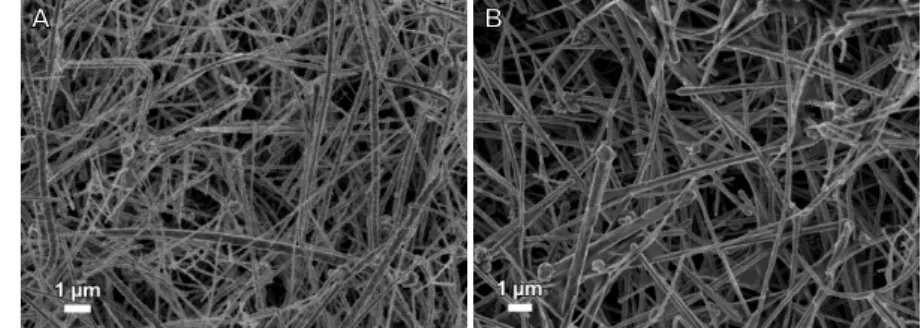
Figure 4.1 – Scanning electron microscopy image of the obtained CuNWs from reaction A (A), B (B), C (C) and D (D). ... 13
Figure 4.2 – Statistical study performed on CuNWs in order to optimize their diameter. A) shows reaction A, B) the reaction with 100 µL of EDA and C) the two hours long reaction. ... 14
Figure 4.3 - Statistical study performed on CuNWs in order to optimize their length. A) shows reaction A, B) the reaction with 100 µL of EDA, and C) the two hours long reaction. ... 14
Figure 4.4 – Structural characterization of CuNWs for reactions A, C and D. ... 14
Figure 4.5 - Photographs from experiments 1 (A), 2 (B) and 3 (C). ... 17
Figure 4.6 – A) Photograph from the results obtained when using tape. B) Microscopic image of the film. ... 18
Figure 4.7 – A) Photograph of the sample with tape, where the arrows indicate the position and the direction of the profilometer measurement on the substrate. B), C) and D) are plots of the profilometer measurements of the respectives arrows. ... 18
Figure 4.8 – Photographs from experiments 5 (A) and 6 (B). ... 19
Figure 4.9 – A) Photograph of the film deposited by spray coating. B) Optical microscopy image from the same film. ... 19
Figure 4.10 – Optical microscopy images from the results obtained with drops of 10 µL. In A) and B) the NWs were dispersed in IPA plus PVP (2 wt%), A) had one deposition and B) four depositions. In C) and D) the NWs were dispersed in IPA plus ethylene glycol (2 wt%), C) had one deposition and D) four depositions. ... 20
Figure 4.11 – Optical microscopy image of the result obtained with a solution of 50 wt% water and 50 % IPA with PVP. ... 20
Figure 4.12 – Optical microscopy image of the result obtained with a solution of IPA with ethylene glycol (2 wt%). ... 21
Figure 4.13 – Photograph showing the difference between Meyer rod (top glass) and newly designed method (bottom glass)... 21
Figure 4.14 – Optical microscopy image of the result obtained with a NWs solution concentration of 7 mg/mL. ... 21
Figure 4.15 – Graphic of the IV curvers obtained for four interdigitateds gaps. ... 22
Figure 4.16 – Graphic of the IV curve before pressure (A) and after applying pressure (B). ... 22
Figure 4.17 – Graphic of the IV curves performed in the same contact. ... 23
Figure 4.18 – A) IV curves of the first two sweeps aplied to the interdigitated contact with 30 µm gap. B) IV curve of the voltage sweep between -40 V and 40 V. ... 23
xiv
Figure 4.20 – IV curves from several depositions and Meyer rod for several interdigitated contacts gaps, A) has 5 µm, B) has 10 µm and C) has 30 µm. ... 24 Figure 4.21 – Photographs showing CuNWs on interdigitated contacts as a conductive medium. Image
A) shows the LED in off state, and image B) shows the LED in ON state. ... 25 Figure 4.22 –Optical miscroscopy images of a CuNWs’ film with aluminum contacts on top. In image
A) an overview of the contact is presented, B) shows a close up, where one may to see that the NWs on the contact area are covered with aluminum. ... 26 Figure 4.23 – Graphic showing the average contact angles of a water droplet on glass and on all the tested surface treatments. ... 26 Figure 4.24 – Optical microscopy image of the results of a glass treated with APTES 0.5 %, followed
five depositions. ... 27 Figure 4.25 – Optical microscopy image of the same film presented in Figure 4.24, with aluminum
contacts on top. ... 27 Figure 4.26 – Graphic showing the profile of an aluminum contact deposited on top of NWs. Inset
shows the contact and the direction of the scanning. ... 27 Figure 4.27 – Graphic showing the transmittance versus wavelength for all five depositions. Inset
show microscopic images from the 5 substrates. ... 28 Figure 4.28 – Graphic showing the transmittance versus wavelength at the visible spectrum for the five
xv
LIST OF TABLES
Table 2.1 – Comparison between ITO and its possible replacement materials. ... 3
Table 4.1 – Parameters of the first drop casting experiment. ... 17
Table 4.2 – Parameters used on experiments 5 and 6. ... 18
Table 4.3 – Parameters varied on doctor blade performed with Meyer rod. ... 20
1
1. MOTIVATION AND OBJECTIVES
1.1.
Motivation
In our modern society, transparent conductors mainly fabricated from indium tin oxide (ITO) are found in a plethora of electronic and optoelectronic devices [1]–[3]. Despite all the attractive features of ITO, the production of this material is starting to suffer the consequences of an extensive mining over the last years, which inflates its price [1][2][4][5]. Besides this, there is a current demand for future applications in electronics, involving low-cost materials and fabrication, and stretchable components. Altogether, these factors are driving forces for the search of reliable alternatives to ITO [2][3].
In order to meet these needs, and taking as a starting point the research already performed on nanowires (NWs), the study of copper nanowires (CuNWs) was established, to take advantage from
copper’s virtues relatively to other metals.
1.2.
Objectives
The main objective of this work is to start a new branch of studies on the field of transparent conductor films. Therefore, the final goal is to create a transparent conductive film of CuNWs. To achieve this, the following aspects are essential:
Study of the effects of the synthesis’ parameters;
Study of several deposition methods;
Study of CuNWs’ inks;
Study of the films’ electrical properties;
3
2. INTRODUCTION
In our daily lives we are surrounded by devices in which the transparency of their conductors is a crucial factor, namely flat panel displays, organic light emitting diodes (OLEDs), photovoltaics (PVs), and touch sensors [1]–[3]. ITO is certainly a very popular ceramic material for the production of transparent conductors, which is attributable to its high transmittance and low sheet resistance [1][2]. Nonetheless, ITO is not free of drawbacks. Because of its ceramic nature, ITO is brittle and, therefore, prone to cracking, which prevents its use in flexible applications [6]–[8]. The scarcity of indium on earth, together with the difficulty in its recycling and the excessive demand of ITO, are additional disadvantages for the broad usage of this material [3]. In fact, the supply of indium was seriously affected by the stoppage of mining from some Chinese companies, which triggered the rise of indium’s
price [4][5]. All these factors inspired the search for ITO’s replacements. Ideally a good replacement should be deposited faster than ITO and have an equal or better electronic and optical performance [7].
2.1.
ITO’s possible replacements
Several materials have been studied aiming the replacement of ITO, from polymers to carbon structures such as carbon nanotubes (CNTs) and graphene, but all of these failed to meet some of the requirements previously mentioned. The major disadvantage of polymers is their inability to stand high currents, a mandatory property in organic photovoltaics (OPVs), since the electrode has to extract charge carriers from the absorbing layer [7]. For CNTs, their optical transmittance is inferior to that of ITO at the same sheet resistance [9]. The production of graphene is a very expensive process in either energy and heavy machinery, since it is grown mainly by chemical vapor deposition at really high temperatures, 650-1000 ℃ [10]. Also, sheet resistance is yet to reach ITO’s level of performance [11].
These studies stimulated the search for new options, which consequently put metals on the spotlight as promising candidates to replace ITO [12]. Metals can be characterized by some specific properties. Those properties are high electrical and thermal conductivity, as well as malleability, ductility, and high reflectivity of light [13]. In addition, when compared to the other materials, the high electrical conductivity of metals makes them the best electrical conductors [12]. The major handicap of metals is their low transparency. Even so, by transforming the metal films into a grid with open holes that allows light’s transmission, their optical performance can be improved. Yet, the cost of such films will raise and these cannot be used in OPVs, neither in OLEDs, since they do not allow flexible applications [9].
Auspiciously metallic NWs appeared as a good alternative to metallic films or grids. Their production can be as simple as a solution phase synthesis, and a transparent film is easily obtained by coating on a transparent substrate. On one hand, noble metals such as silver and gold could be an option to produce NWs, since these materials in such shape display similar resistivity to their bulk counterparts. However, both metals are expensive [14]. On the other hand, copper is more abundant and cheaper than silver or indium, and its conductivity is only 6 % lower to that of silver [3][14][15].
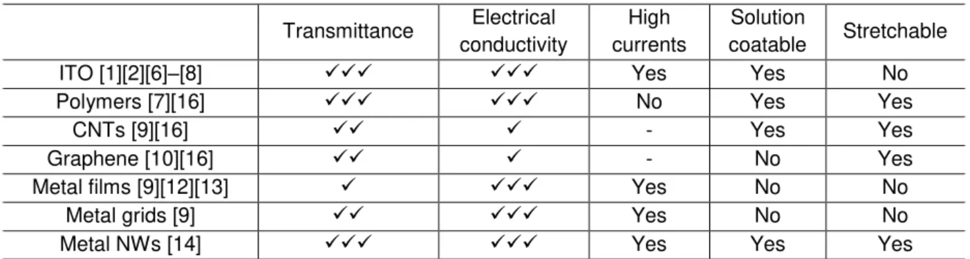
Table 2.1 establishes the main differences between all previously referred materials. Table 2.1 – Comparison between ITO and its possible replacement materials.
Transmittance Electrical conductivity
High currents
Solution
coatable Stretchable
ITO [1][2][6]–[8] Yes Yes No
Polymers [7][16] No Yes Yes
CNTs [9][16] - Yes Yes
Graphene [10][16] - No Yes
Metal films [9][12][13] Yes No No
Metal grids [9] Yes No No
4
2.2.
Copper and copper nanowires
Copper is mankind’s oldest metal, dating back some 10 000 years. All the great civilizations of the past used copper and its alloys. Though, it was in the Industrial Revolution that copper and copper alloys faced a remarkable change in their way of production and consumption [17].
Since copper belongs to group 11 of the periodic table, this means it has certain attributes: it has one s-orbital electron on top of a filled d-electron shell and is characterized by high ductility and electrical conductivity. The filled d-shells in this element do not contribute much to the interatomic interactions, which are dominated by the s-electrons through metallic bonds. Unlike metals with incomplete d-shells, metallic bonds in copper are lacking a covalent character and are relatively weak. This explains the low hardness and high ductility of copper single crystals. Furthermore, copper alloys are widely used, because they have unique mechanical and physical properties in addition to excellent corrosion and wear resistance [18]. Given that a material can change its properties at nanoscale and be affected by quantum effects, there has been some discussion on whether CuNWs would have a similar resistivity compared to its bulk material [19].
CuNWs’ conductivity is in conflict with their transmittance: when one increases, the other decreases [8]. A compromise between both phenomena must be reached. In a NW film, conduction is due to electrons percolation across a path of interconnected NWs. There are some important parameters to achieve percolation: NW’s concentration, length, and homogeneity. Since the contact resistance is much higher than the resistance of a single NW, long NWs are much more desirable instead of a big density of NWs [9].
2.3.
Synthesis of copper nanowires
Several routes may be used to synthesize CuNWs. In the case of electrospinning and vapor deposition, the expensive machinery required for their execution and the difficulty in scaling up these techniques represent their major drawbacks. Chemical solution arises as a viable and popular alternative, having been adopted by numerous labs. The main approaches used are an ethylenediamine (EDA) mediated synthesis [2][5][20] and an alkylamine mediated synthesis [8][21][22]. A comparison between the results found in the main studies is shown in Figure 2.1.
Figure 2.1 – Graphic showing some of the results obtained so far by other research groups. In Chang et al. [20] the average values were considered. Shi et al. [21] did not fully specify the CuNWs length and the diameter was an average of the results presented. Zhang et al. [22] also did not fully specify the CuNWs length [2][5][8][23]–[26].
5
by the addition of polyvinylpyrrolidone (PVP), which avoids the formation of aggregates, and letting the CuNWs grow in an ice bath [24]. Ye et al. [2] studied the effect of all parameters very deeply. They were able to rise the CuNWs’ aspect ratio up to 2300. The resulting CuNWs had an average length of 80 µm, with some of those CuNWs reaching 200 µm, whereas the average diameter was 35 nm. Inspired by the previous reactions, Chen et al. [25] were able to obtain NWs with lengths between 20-30 µm and diameters of 50 nm. The main difference to the preceding reactions was the adding of the reagents in an ice bath. More recently, Ye et al. [23] decided to study the reaction kinetics and achieved CuNWs with 35 nm of diameter and 63 µm of length. At Centro de Investigação de Materiais (CENIMAT), Nunes et al.[26] achieved NWs with an average length of 10 µm and an average diameter of 250 nm, using copper acetate instead of copper nitrate in Chang’s method [20].
Shi et al. [21] used an alkylamine mediated synthesis in which octadecylamine had a double function: to promote the reduction of copper ions and to work as a capping agent. The as-produced CuNWs were several millimeters long and displayed 30-100 nm in diameter. Zhang and coworkers [22] reported a nonaqueous synthesis of CuNWs by self-catalysis in which the CuNWs were grown in a tubular medium, created by the mixing of hexadeceylamine and cetyltriamoninum bromide. The research group also noted the need to use platinum, responsible for the catalysis of the copper ions’
reduction. These CuNWs had lengths from tens to hundreds of micrometers and the diameter was ca. 78 nm. Guo et al. [8] used oleylamine instead of octadecylamine, and nickel ions (Ni2+) as catalyst for copper reduction. The CuNWs had an aspect ratio of 2500, with lengths of 40 µm and an average diameter of 16 nm. In this synthesis, copper ions come from Copper (II) chloride dihydrate, and chloride ions lead to an anisotropic growth.
2.4.
Fabrication of copper nanowires films
One may choose amongst different deposition methods to produce transparent conductor films, such as drop casting [27]–[29], Meyer rod coating [2][15][24], spray coating [29]–[31], and vacuum filtration [5][8], as presented in Figure 2.2.
Figure 2.2 – Representation of drop casting A), Meyer rod coating B), spray coating C) and vacuum filtration D).
Drop casting is a simple technique in which a small volume of a solution with NWs is placed
on top of the substrate and dried. Drying happens by solvent’s evaporation with or without temperature [27]–[29]. Meyer rod coating comprises dragging a NWs’ ink throughout the substrate
with a Meyer rod. This is a very simple method, and lately the most common inks use nitrocellulose, which is very volatile and has a low evaporation temperature. So, it can be taken off with plasma cleaning and through heating in an oven [24]. More recently, Kang et al. [32] adapted the previous method and deposited NWs with polydimethylsiloxane nanochannels. The main goal of this new method is to produce films of aligned NWs. Spray coating consists of using an airbrush to deposit NWs. A solution with NWs is used and normally this technique requires a hot plate to evaporate the small drops, which are sprayed on the substrate. The drops size can be controlled by the pressure of the gas that flows inside the sprayer [29]–[31]. Vacuum filtration has some similarities with drop cast, however, the solvent is deposited on a filter membrane instead of being deposited on the final substrate. After vacuum, the NWs’ film on the filter membrane will be transferred to the final substrate [8].
6
2.5.
Reduction of the contact resistance between copper nanowires
CuNWs have a high tendency to oxidize in air, compared to bulk Cu, because the surface area is drastically increased. Such fact makes it more difficult to reduce the contact resistance. Nevertheless, protection from oxidation is discussed in Chapter 2.6.
The most common ways to reduce contact resistance are based on the exertion of a pressure on top of the NWs [11] and thermal annealing [33] (Figure 2.3 A and B).
Figure 2.3 – Representation of some methods to reduce contact resistance. A) Mechanical pressure, B) thermal annealing, C) plasmonic laser welding and D) acid treatments.
Hu et al. [11] used two glass slides with a film of silver nanowires (AgNWs) between two metal plates. By pressing the metal plates through a mechanical manual pressure, the group was able to decrease the sheet resistance from hundreds to tens of Ω sq−1, while the surface roughness was
diminished as well. Thermal annealing at 200 ℃ for 20 minutes has been shown to significantly reduce the sheet resistance of a NWs’ film [33]. However, annealing is not ideal because it requires temperatures above 100 ℃, which might induce oxidation of CuNWs.
Recently, researchers have been studying two new possibilities to counter oxidation: plasmonic laser welding [34], and acid treatments on the surface of CuNWs [35]. Han and co-workers [34] designed a plasmonic laser with fast scanning speed, which made possible the suppression of the oxidation problem during annealing of Cu. Acid treatments are able to remove the oxide from the CuNWs’ surface and allow the possibility of integration in roll-to-roll processing.
2.6.
Protection from oxidation
NWs require protection from atmospheric corrosion, given that CuNWs react with oxygen very easily and, as a consequence, they get more resistive.
Rathmell and co-workers [24] coated CuNWs films with a nitrocellulose-based ink in order to protect the NWs from oxidation. Afterwards the nitrocellulose was removed with plasma cleaner, leaving a highly conductive CuNWs network. The same researchers demonstrated a method for synthesizing CuNWs with nickel shells. Cupronickel NWs showed a higher resistivity than CuNWs. Also, since nickel covers copper, the diameters of the NWs increased to 200-300 nm. Despite this increase, which lowered the performance of the transparent conductive films, the sheet resistance increased by only 10 Ω sq−1 after 30 days [15]. More recently, CuNWs were coated with a metal, zinc,
tin, or indium, by electroplating. This process was followed by oxidation to create oxides shells that protected the NWs, without degrading conductivity and transmittance of the films [3].
Han et al. [14] demonstrated a novel method to reverse copper oxidation through photothermochemical reduction. After the CuNWs are deposited in a film, they were oxidized by thermal oxidation. Ethylene glycol was posteriorly coated on top of the NWs, working as a reducing agent. Then the oxidized NWs were irradiated by a focused laser beam. The laser was generated by a diode-pumped solid-state Nd:YAG laser, because the wavelength is higher than copper oxides’
bandgaps.
Pressure ℃
7
2.7.
Highly stretchable and foldable electrodes
Various new materials have been studied to be used as stretchable and foldable electrodes, such as conducting polymers, CNTs, and graphene [16]. Nevertheless, they have shown limited applications and performance, because conductive polymers demonstrated poor stability and conductivity, and carbon-based nanomaterial revealed low electrical conductivity and high material cost [16]. To the
author’s knowledge there has not been much research on stretchable and foldable electrodes of CuNWs. Fortunately, Lee et al. made a breakthrough research with AgNWs, since they were able to get a highly stretchable and highly conductive NW percolation network. The network had a superior electrical conductivity and mechanical compliance compared to CNTs and graphene. To achieve such results the key factor was the NWs length [16].
2.8.
Device Integration
Since markets for transparent conductors continue to grow and there is a demand for new materials, the next step for CuNWs is device integration. With that in mind, Sachse and co-workers [36] demonstrated a small-molecule organic solar cell with a transparent electrode of CuNWs. This cell revealed perfect electrical behavior with 3.1 % efficiency compared to 4.0 % for an ITO reference device. Then, Stewart et al. [35] used CuNWs, protected with nickel to prevent oxidation, as a conductor in an OPV. The device had an efficiency of 4.9 % compared to 7.1 % of ITO. The lower transmittance of the copper-nickel film could explain the lower efficiency of the device produced in the study. Later, Chen et al. [25] demonstrated an OPV with a contact of poly(3,4-ethylenedioxythiophene):polystyrene sulfonate (PEDOT:PSS), with CuNWs coated on it. This contact had a low surface roughness.
9
3.
MATERIALS AND METHODS
3.1.
Copper nanowires synthesis
Two syntheses were tested, one using copper acetate and another one with copper nitrate. Both methods produce NWs via chemical reaction.
3.1.1.
Synthesis using copper acetate
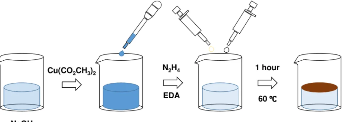
NWs were produced following Nunes et al. [26] method. First, 24 g of sodium hydroxide (NaOH) was dissolved in 40 mL of water, raising water’s temperature above 80 ℃. The solution was kept under stirring while 0.46 g of copper(II) acetate was dissolved in 20 mL of water. Then, after 15 minutes, 1.5 mL of copper acetate’s solution was added to the NaOH solution in a dropwise manner, because the NaOH solution was still hot. Subsequently, 50 μL of EDA and 10 μL of hydrazine were also added to the previous solution. Afterwards, the solution was placed in a hot bath at 65 ℃ for one hour. This process is illustrated in Figure 3.1.
Figure 3.1 – Schematic of the reaction of CuNWs production troughout all the phases.
3.1.2. Synthesis using copper nitrate
This synthesis is based on a method developed by Rathmell et al. [5]. To start, 24 g of sodium hydroxide (NaOH) were dissolved in 40 mL of water and kept under constant stirring at 400 rpm. Another solution was prepared by dissolving 0.93 g of copper(II) nitrate hemi(pentahydrate) in 20 mL of water. After 10 minutes, 2 mL of this solution was added dropwise to the previous NaOH solution. Then, 600 μL of EDA and 50 μL of hydrazine (35 wt%) were added to the NaOH solution, and kept under stirring for 1 minute at 700 rpm. Subsequently, the solution was left in a hot bath at 80 ℃ for one hour (Figure 3.2).
Figure 3.2 – Schematic of the CuNWs synthesis in all phases of the reaction.
NaOH
Cu(CO2CH3)2 N2H4
EDA
1 hour 60 ℃
NaOH
Cu(NO3)2·2.5H2O EDA
N2H4
1 hour
10
3.1.3. Materials and reagents
NaOH was obtained from Fisher Scientific. Copper(II) acetate was acquired from Sigma-Aldrich. For the copper acetate reaction, EDA (99 %) was purchased from Merck. Copper(II) nitrate hemi(pentahydrate) and EDA (75-80 %) were purchased from Sigma-Aldrich. Both syntheses were made with the same hydrazine (65 wt%, Sigma-Aldrich), but for the copper nitrate synthesis, water was added to create hydrazine with 35 wt%. Deionized water (Millipore) was used.
3.1.4. Cleaning and dispersion of the nanowires
NWs were cleaned with isopropyl alcohol (IPA, Sigma-Aldrich) and deionized water (Millipore). Centrifugation was used in the cleaning process with runs of 5 minutes at 4000 rotations per minute (rpm), as illustrated in Figure 3.3 A.
Sonication was performed to NWs in IPA, in order to disperse them. The ultra-sonication was made with a cylindrical tip (3 mm end cap diameter) for 2 minutes in a UP400S sonicator, using an amplitude of 40 %. After sonication, the NWs were kept under stirring at 350 rpm, as demonstrated in Figure 3.3 B.
Figure 3.3 – Cleaning steps representation. A) represents centrifugation and B) sonication.
3.1.5. Characterization of copper nanowires: morphological and structural analysis
The morphological analysis of CuNWs was performed via scanning electron microscopy (SEM). The workstation was assembled by Carl Zeiss Auriga, and it is equipped with a Carl Zeiss Auriga crossbeam (SEM-FIB) and with an Oxford X-ray energy dispersive spectrometer. An optical microscope (Olympus BX51) equipped with an Olympus DP50 camera, followed by the Cell F View Image System Software, used to obtain images of the NWs, since they are long enough to be visible in the previous equipment. ImageJ software was used to determine the dimensions of the CuNWs from both SEM and optical microscope images.
Analysis of the CuNWs structure was carried by X-ray diffraction (XRD) using a
PANalyticalX’Pert Pro X-ray diffractometer in Bragg–Brentano geometry, with a monochromatic Cu-Kα
radiation source (wavelength 1.5406 Å). XRD measurements were carried out from 30° to 90º (2θ),
with a scanning step size of 0.033°.
3.2.
Copper nanowires films
3.2.1. Materials and reagents
In drop cast a micropipette was used, as well as a hot plate and glass (VWR). Glass comes in squares of 10 cm × 10 cm and were cut in smaller pieces of 2 cm × 2 cm. Then the smaller glasses were cleaned in an ultrasounds’ bath, first 15 mins in IPA, followed by 15 mins in acetone and finally 15 mins in water, the bath temperature was 60 ℃ for all. For spray coating the same type of glasses’
2 cm × 2 cm were used with the same cleaning process. In doctor blade the glasses used had 7 cm × 2 cm, while the interdigitated were bigger and thinner. Films were deposited by a film applicator from BYK, which supplements also came from BYK. The gold interdigitated contacts were
11
made by depositing photoresist on a glass, then exposing the photoresist to ultraviolet (UV) light, followed by photoresist’s revelation. Afterwards, a thin layer of titanium was deposited by e-beam to create a good adhesion to Corning glass, followed by a deposition of gold, also by e-beam. Then the contacts were completed by lift-off.
To avoid aggregates during the study of NWs solutions, ethylene glycol (MW = 62,07 g/mol) from Carlo Erba reagents was used, as well as ethanol (EtOH) absolute from Fisher Scientific, and PVP (MW = 10 000 g/mol) from Sigma-Aldrich.
Silanization on glass was performed through two routes: chemical reaction and vacuum. To perform the chemical silanization, (3-aminopropyl)triethoxysilane (APTES) from Sigma-Aldrich was used, as well as EtOH absolute from Fisher Scientific. Three solutions were prepared with different weight percentage of APTES, and a glass was placed in a solution for ten minutes. Vacuum silanization was made by using trichloro(1H, 1H, 2H, 2H-perfluorooctyl)silane (97 %) from Sigma-Aldrich, with a vacuum pump from KNF Neuberger and a plastic desiccator. Glasses were placed in a vacuum container. Afterwards, three droplets of trichloro(1H, 1H, 2H, 2H-perfluorooctyl)silane were placed in a plastic Petri dish and the vacuum pump was kept on for 30 minutes. Then the vacuum pump was turned off and vacuum was maintained for three hours. UV-treatment was performed with NOVASCAN (PSD-UV) for one hour. The UV-light generated has two peaks, 185 nm and 254 nm.
3.2.2. Characterization of copper films: morphological, electrical and optical analysis
Films were morphologically analyzed by optical microscope (Olympus BX51) equipped with an Olympus DP50 camera, followed by the Cell F View Image System Software.
Electrical characterization was done by the two probes method, using Keysight B1500A with Cascade Microtech EPS150 at room temperature and in a dark room. The four probes method is more accurate, since each probe measures just one quantity, either voltage or current. Because the probes set to measure voltage have high input impedance, the current flowing through them is very low. However, applying the four probe method to the interdigitated is more complex.
Optical characterization was performed with a Perkin Elmer Lambda 950 UV-Vis-NIR Spectrophotometer. Measurements were performed between 250 nm and 2500 nm, with a step of 5 nm, by using the integrating sphere.
3.2.3. Contact angles measurement
13
4.
RESULTS AND DISCUSSION
4.1.
Copper nanowires synthesis
Firstly, CuNWs were produced using copper acetate, since they were previously used in CENIMAT,
however this synthesis wasn’t study very deeply. More recently, a new synthesis was designed using
copper nitrate.
4.1.1. Synthesis using copper acetate
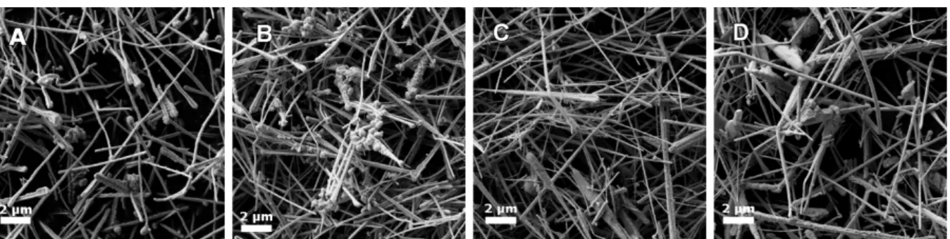
In order to study the variation of the aspect ratio (length/diameter), three parameters were tested, namely hydrazine, EDA, and time. In these syntheses EDA works as a capping agent and hydrazine as a reducing agent. Since EDA is the capping agent, an augment of EDA should promote thinner NWs. Increasing the amount of hydrazine leads to an increase of CuNWs’ diameter. This can lead to less resistive NWs, however their optical properties will be worse. The first reaction (Reaction A, Figure 4.1 A) was conducted as shown in Chapter Methods. The NWs produced showed a cylindrical shape and had an average diameter of 256 nm. Then another reaction was produced, this time with 15 µL of hydrazine (Reaction B), while the other parameters were maintained. The increase of hydrazine (5 µL more than Reaction A) led to the formation of NWs with greater thickness (272
nm)
. Furthermore, these NWs exhibited some clusters, as shown in Figure 4.1 B. Therefore, the NWs did not present the desired results and were not analyzed further ahead.Afterwards, an alternative reaction was prepared, only varying the amount of EDA (Reaction C, Figure 4.1 C). The quantity of EDA added was 100 µL (doubling the quantity comparatively to Reaction A). The resulting NWs were thinner compared to those from first reaction, albeit some tapered effect was noticed. In the last attempt to maximize the CuNWs aspect ratio, the
synthesis’ duration was increased by one hour, resulting in a two hours long reaction (Reaction D, Figure 4.1 D).
Figure 4.1 – Scanning electron microscopy image of the obtained CuNWs from reaction A (A), B (B), C (C) and D (D).
14
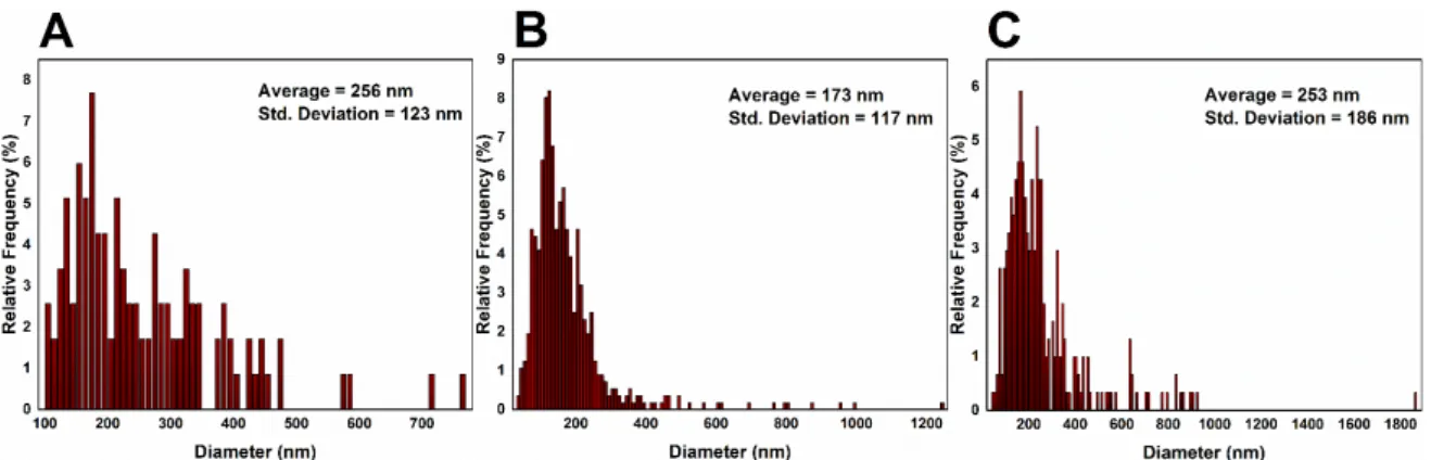
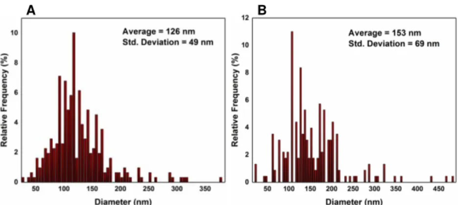
Figure 4.2 – Statistical study performed on CuNWs in order to optimize their diameter. A) shows reaction A, B) the reaction with 100 µL of EDA and C) the two hours long reaction.
Then the length of the NWs was studied (Figure 4.3) and again the results for the two hours long reaction are unexpected, showing there is no improvement in the CuNWs’ average length for longer reactions. The reaction with more EDA exhibited an improvement in the CuNWs average length. Nonetheless, the standard deviation also increased.
Figure 4.3 - Statistical study performed on CuNWs in order to optimize their length. A) shows reaction A, B) the reaction with 100 µL of EDA, and C) the two hours long reaction.
CuNWs formed from reaction A achieved an aspect ratio of 43, which was increased to 68 with reaction B since the length of the NWs increased and the correspondent diameters decreased.
The XRD patterns of CuNWs shown in Figure 4.4 exhibited a big presence of copper (111) plane in all three reactions (ICDD File: 00-004-0836). CuO’s (111) plane (ICDD File: 01-080-1917) is present as well, and reaction D also had some evidence of Cu2O’s (111) plane (ICDD File: 01-077-0199).
15
Increasing the amount of EDA added to the solution reduced the NWs diameter and increased their lengths, leading to an increase of the aspect ratio, which according to literature, will reduce their resistance. Nevertheless, the relative frequency for sizes between 0 µm and 5 µm for about 5 %, as well as the presence of CuO’s (111), also increased, and oxidation is very undesired in CuNWs. Copper itself has already a strong capability to oxidize, so, since the increased sizes of the NWs was not very vast, we decided to take a conservative way and use the NWs from reaction A.
4.1.2. Synthesis using copper nitrate
NWs were produced as described in Chapter Methods. In this synthesis, a supernatant is formed after 15 minutes when the solution is left at the water bath. Having this in mind, some NWs were collected after 20, 30 and 60 minutes, to understand if the synthesis time could be lowered.
Figure 4.5 – Scanning electron microscopy image of CuNWs after 20 minutes.
Figure 4.5 shows that NWs are suffering some nucleation, which means they are still maturing.
Figure 4.6 – Scanning electron microscopy image of CuNWs after 30 minutes (A) and 60 minutes (B).
NWs appear to exhibit smaller diameters in Figure 4.6 A in comparison to Figure 4.6 B. However, some nucleation was still found after 30 minutes as shown in Figure 4.7.
Figure 4.7 – Scanning electron microscopy image of CuNWs after 30 minutes, where some undergoing nucleation is visible.
16
Figure 4.8 – Statistical study performed on CuNWs in order to optimize their diameter. A) shows the 30 minutes and B) the 60 minutes long water bath.
Indeed, longer water bath times increase the average diameter of the CuNWs (Figure 4.8), however, they also increased the NWs length (Figure 4.9), with some NWS achieving lengths of more than 60 µm.
Figure 4.9 – Statistical study performed on CuNWs in order to optimize their length. A) shows the 30 minutes and B) the 60 minutes long water bath.
Afterwards, a structural characterization of the CuNWs with 60 minutes long water bath was performed. The same characterization was not performed to the other NWs, because the increased length of the NWs with 60 minutes long water bath is so great that makes the other CuNWs, with shorter water baths, unviable to use.
Figure 4.10 – Structural characterization of CuNWs.
XRD pattern of the CuNWs shown in Figure 4.10 only displayed the presence of copper planes (ICDD File: 00-004-0836).
These results are superior to the results obtained in the synthesis with copper acetate, since the aspect ratio was increased to 128. However, this new synthesis took some time to be fully functional and could not be tested electrically and optically.
A B
A B
30 40 50 60 70 80 90
(3 1 1 ) (2 2 0 ) (2 0 0 ) In te n s it y ( a .u .)
17
4.2.
Deposition methods
With the intention of getting a film of NWs deposited on glass, several deposition methods were tested. These methods were: drop casting, spray coating, and doctor blade. In all the methods the NWs used were with copper acetate.
4.2.1. Drop Casting
A starting test consisting of three experiments was carried with the conditions showed in Table 4.1. The NWs were stored in IPA and since IPA has a low boiling point (82.6 ℃), no temperature was used to evaporate it. An experiment schematic can be found in Annex A.
Table 4.1 – Parameters of the first drop casting experiment. Experiment Number of drops Drop volume (µL)
1 10 10
2 10 5
3 10 20
The results of the test can be seen in Figure 4.11. The area of the NWs’ film deposited is dependent on the drop quantity, so the smaller the drop quantity the smaller the area occupied by NWs. Interestingly, the first drop will spread more than its predecessors. Moreover, the drops after the first one will clean some NWs deposited on the center of the film to the drop boundary. This leads to
the creation of some “rings”, where the agglomeration of NWs is much denser compared to the average of the film.
Figure 4.11 - Photographs from experiments 1 (A), 2 (B) and 3 (C).
In an attempt to control the area of the droplet spread, two possibilities were taken into account. One possibility was limiting the glass, so that the drop would not be free to spread, and the other one was adding temperature to promote a faster evaporation of IPA.
Four pieces of adhesive tape were placed on top of a glass leaving a square in the middle, then six drops of 5 µL of NWs solution were deposited. As seen in Figure 4.12 A, the main objective of this try was not reached, since there was a poor spread of the droplets. Due to the tape thickness, roughly 35 µm, when two pieces are overlapping it creates a space where the drop is free to move. It was also noticeable that tape presented a weird effect at the edges, since there is a sudden raise of height, and the effect of barrier is lost (Figure 4.13). Furthermore, the CuNWs were poorly dispersed and started to form some aggregates (Figure 4.12 B).
18
Figure 4.12 – A) Photograph from the results obtained when using tape. B) Microscopic image of the film.
Figure 4.13 – A) Photograph of the sample with tape, where the arrows indicate the position and the direction of the profilometer measurement on the substrate. B), C) and D) are plots of the profilometer measurements of the respectives arrows.
Afterwards, the effect of the temperature was tested. The selected temperature was 40 ℃
because a higher temperature will evaporate IPA very fast, and the NWs will be dispersed in an undesired pattern (Table 4.2).
Table 4.2 – Parameters used on experiments 5 and 6.
Experiment Number of drops Drop volume (µL)
5 10 10
6 10 5
Comparing the first experiment to the fifth experiment, the NWs solution was visibly spread very easily on top of glass for both experiments. However, in the fifth experiment there is a small circle in the middle of the glass with higher transparency (Figure 4.14 A).
A
B
A
B
19
Figure 4.14 – Photographs from experiments 5 (A) and 6 (B).
Lowering the drop volume generated a much darker and small film, although the “coffee ring”
effect was still present (Figure 4.14 B).
4.2.2. Spray coating
A small test was conducted aiming to check the viability of spray coating in terms of reproducibility and control. The spray gun pressure was set to 15 psi with N2 gas, the distance between the glass substrate and the gun was 10 cm, and the substrate was under constant heating at 60 ℃.
Figure 4.15 – A) Photograph of the film deposited by spray coating. B) Optical microscopy image from the same film.
The deposition by spray coating had no uniformity and created a lot of aggregates (Figure 4.15). To increase the film’s uniformity, the sprayer would require some circulatory movements, in
order to spray the NWs all along the surface. However, there is no machinery available in the lab to perform those movements. The same can be made by hand, but that will add the human error. So this deposition method was abandoned.
4.2.3. Doctor blade
To perform doctor blade a Meyer rod was used to spread the NWs on top of a glass substrate, which was seven centimeters length and two centimeters height (Annex B). The CuNWs were dispersed in IPA, in a concentration of 1 mg/mL, and the bar moved at a speed of 50 mm/s. Previously to the deposition, a UV treatment was carried on top of the glass substrate during 15 mins, followed by several depositions done in that glass substrate to understand how this can influence the number of CuNWs deposited.
Avoiding aggregates is essential to reach low transparency. In other words, a good dispersity of the NWs could lead to better transparent conductors. Having this in mind, higher viscosity solutions were considered as probable improvers of dispersity. Three parameters were varied, the number of depositions in the same substrate, drop quantity, and storing solution (Table 4.3).
A
B
20
Table 4.3 – Parameters varied on doctor blade performed with Meyer rod. Solution Number of depositions Drop quantity (µL)
IPA + PVP (2 wt%)
1 25
2 25
1 10
4 10
IPA + ethylene glycol (2 wt%)
1 25
2 25
1 10
4 10
From all the results obtained, the ones shown ahead in Figure 4.16 were the best and all of them were made with drops of 10 µL. Additionally, the best storing solution was IPA with ethylene glycol (2 wt%). When the NWs were used in a solution of IPA with PVP (2 wt%), some aggregates were generated even with just one deposition. Also, the presence of PVP is noticeable around the NWs, so a further process would be needed to clean it, the most common being plasma treatment.
Figure 4.16 – Optical microscopy images from the results obtained with drops of 10 µL. In A) and B) the NWs were dispersed in IPA plus PVP (2 wt%), A) had one deposition and B) four depositions. In C) and D) the NWs were dispersed in IPA plus ethylene glycol (2 wt%), C) had one deposition and D) four depositions.
Subsequently a new solution was tried, using the former solution of IPA with PVP (2 wt%) to create a solution with 50 wt% water and 50 wt% IPA with PVP. Yet, like the solution without water, this one also generated some aggregates, which were visible after one deposition, as shown in Figure 4.17.
Figure 4.17 – Optical microscopy image of the result obtained with a solution of 50 wt% water and 50 % IPA with PVP.
21
Figure 4.18 – Optical microscopy image of the result obtained with a solution of IPA with ethylene glycol (2 wt%).
Nevertheless, to obtain a conductor, several NWs would need to be in touch, and looking back at the results, even with four depositions on the same substrate, this goal was far from reachable. So, by switching the main focus from transparency to conductivity, a new method was verified. This new method uses one of the supplements for doctor blade. A piece of glass was taped to the back of the supplement, but just on top, letting the bottom of the glass to move freely, as shown in Annex C.
A comparison study between the Meyer rod and this new method was conducted, by using a solution of NWs in IPA with the same 1 mg/mL concentration, a drop volume of 10 µL, and without UV treatment.
Figure 4.19 – Photograph showing the difference between Meyer rod (top glass) and newly designed method (bottom glass).
In Figure 4.19, the difference between the two methods after five depositions is shown, the reddish color is more present in the glass where the newly designed method was used. Afterwards,
the solution’s concentration was increased to 7 mg/mL and a new film was deposited, again using the same conditions as before (Figure 4.20).
Figure 4.20 – Optical microscopy image of the result obtained with a NWs solution concentration of 7 mg/mL.
This effort exhibits the best results so far and the deposited film could be conductive, because it shows that a few CuNWs are creating a path.
4.2.3.1. Electrical characterization
22
contacts. The schematic of the interdigitated contacts can be seen in Annex D. The interdigitated contacts had a length (L) of 4.2 mm, while the width (W) and the space between electrodes (S) were equal. The interdigitated with gaps of 5 µm have 300 contacts, the 10 µm have 150, 30 µm possess 50, and finally the 50 µm hold 30 contacts. In all the depositions, it was assured that the solution spread through all the contacts. Then a film of CuNWs was deposited on glass, first with bottom contacts, afterwards with top contacts.
4.2.3.1.1. Nanowires on interdigitated contacts
Using the same parameters as stated before, of five depositions with a highly concentrated solution (7 mg/mL), drop volume of 10 µL, and a deposition speed of 50 mm/s, a conductive path was generated on the 5 µm and 10 µm separated interdigitated contacts. Among the 30 µm and 50 µm interdigitated contacts there was no conductive channel as the results in Figure 4.21 suggest.
Figure 4.21 – Graphic of the IV curvers obtained for four interdigitated gaps.
The interdigitated contact with 5 µm showed a very linear performance right away, as a typical behavior expected for a conductor, having a resistance of 37.75 Ω.
All the interdigitated contacts with 10 µm were functional, although they did not exhibit a fully ohmic behavior. This could be due to contact resistance, between NWs and between the NWs and the contact itself. So the Meyer rod was used throughout the sample just to apply pressure on the NWs and after another electrical measurement, the NWs displayed an ohmic behavior (Figure 4.22).
Figure 4.22 – Graphic of the IV curve before pressure (A) and after applying pressure (B).
The resistance was calculated by Ohm’s law, and although some contacts dropped in resistance, others increased, which makes it impossible to find a correlation between pressure and resistance. Another interesting effect is shown in Figure 4.23. In the first voltage sweep, the calculated resistance was 65.20 Ω. However, in the last voltage sweep, the resistance decreased to 30.62 Ω,
23
inducing the presence of an activation energy. Throughout the voltage sweep, the absence of NWs’
hysteresis is notorious, which is the expected behavior of a conductor.
Figure 4.23 – Graphic of the IV curves performed in the same contact.
The Meyer rod was also used on the contacts with 30 µm. Having in mind that NWs might need some activation energy, and after some measurements in which they were not conducting, a voltage sweep between -40 V and 40 V was applied to the contacts, which made the NWs’ film
conductive (Figure 4.24).
Figure 4.24 – A) IV curves of the first two sweeps aplied to the interdigitated contact with 30 µm gap. B) IV curve of the voltage sweep between -40 V and 40 V with compliance set to 20 mA.
At this point a new sweep was done to analyse the resistance of the contact, consisting in a voltage sweep between -1 V and 1 V. The curve shows a perfectly ohmic behaviour and a resistance of 71.89 Ω, which is slightly higher compared to the interdigitated contacts with less gap (Figure 4.25).
-2 -1 0 1 2
-1.0x10⁻¹ -8.0x10⁻² -6.0x10⁻² -4.0x10⁻² -2.0x10⁻² 0.0 2.0x10⁻² 4.0x10⁻² 6.0x10⁻² 8.0x10⁻² C u rr e n t (A ) Voltage (V) 65.20
37.45 30.62
24
Figure 4.25 – IV curve done to the contact with 30 µm gap from -1 V to 1 V.
After this, a new study was conducted to check the contacts performance throughout the depositions. Five depositions were done on the contacts with gaps between 5 µm, 10 µm and 30 µm, and a final passage with the Meyer rod was performed to apply pressure on the NWs.
Figure 4.26 – IV curves from several depositions and Meyer rod for several interdigitated contacts gaps, A) has 5 µm, B) has 10 µm and C) has 30 µm.
The interdigitated with spacing of 5 µm were conductive in almost every deposition except from the 4th deposition, which might be due to some undesired particles on the glass surface that could be dragged with the deposition (Figure 4.26 A). Other than that, the highest resistance was 269.54 Ω.
A
B
25
Table 4.4 – Resistances calculated for the performed depositions.
Interdigitated’s gap 5 µm 10 µm 30 µm
1st deposition 65.10 Ω 108.58 Ω 201.21 Ω
2nd deposition 119.76 Ω 92.34 Ω 207.04 Ω
3rd deposition 269.54 Ω 164.74 Ω 1.6×10⁹Ω 4th deposition 2.65×10⁸Ω 44.00 Ω 1.6×10⁸Ω
5th deposition 60.13 Ω 48.36 Ω 2.8×10⁸Ω
Meyer rod 68.07 Ω 46.19 Ω 71.84 Ω
On the 10 µm spaced interdigitated the resistance was always lower than 200 Ω, however, the ones with higher resistance demonstrated a weird behavior that is not expected from a conductor (Figure 4.26 B). The interdigitated with a gap of 30 µm managed to score a resistance near 200 Ω. Such fact could be due to some long NW given that, as shown before, NWs lengths can reach up to ca. 35 µm (Figure 4.26 C). That same wire maintained its initial position during the second deposition, but eventually it got moved with the other depositions, resulting in a resistance increase. However, with more passages, more NWs are deposited, increasing the possibility of creating a conductive path. The conductive path was established with the Meyer rod, which must have drastically decreased the contact resistance between NWs (Table 4.4). Interestingly, the resistance per gap distance in the first
deposition decreased with the gaps’ augment. The resistance per gap distance (first deposition) for 5 µm, 10 µm and 30 µm was 13.02 Ω/µm, 10.86 Ω/µm and 6.71 Ω/µm, respectively. However, further studies are required to take conclusions about this behavior, because there are a lot of uncontrolled variables, such as number of NWs between contacts.
Previously the Meyer rod was able to lead to a fully ohmic behavior, and now its usage produced a fully functional contact. These finding point to the fact that the function of the Meyer rod is purely to apply pressure on the NWs.
There is no clear correlation between the number of depositions and resistance of NWs’ film.
Figure 4.27 – Photographs showing CuNWs on interdigitated contacts as a conductive medium. Image A) shows the LED in off state, and image B) shows the LED in ON state.
Figure 4.27 shows a possible application for CuNWs on interdigitated contacts. Once the needed voltage is supplied to the system (Figure 4.27 B), a LED is turned ON due to the current flowing through the CuNWs, placed between the interdigitated contacts.
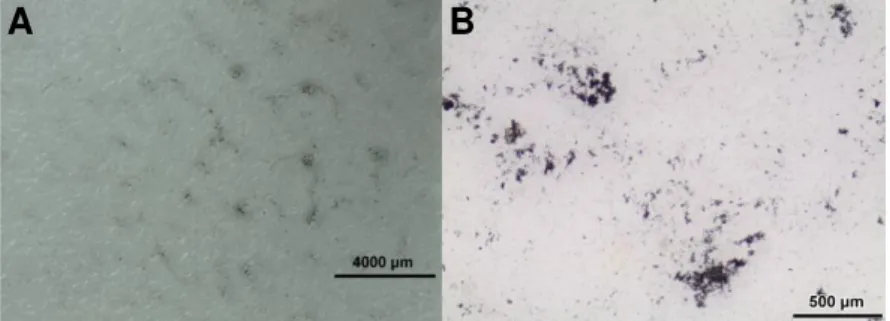
4.2.3.1.2. Conductive copper nanowires films
The films created with the same parameters as those pointed out in Chapter 4.2.3.1.1 were not conductive, so the number of depositions was increased to ten, leading to a very dense mesh. Figure 4.28 shows the highly dense mesh with aluminum contacts on top, where the aluminum pads are separated by 160 µm. However, there was no improvement in terms of conduction, which could be due to a high resistance between the NWs. Hence, the NW’s film was pressed with a Meyer rod
which, nevertheless, produced no improvement. Thus, a piece of glass was placed on top of the film to apply pressure on it, aiming to make it conductive.
26
Figure 4.28 – Optical miscroscopy images of a CuNWs’ film with aluminum contacts on top. In image A) an overview of the contact is presented, B) shows a close up, where one may to see that the NWs on the contact area are covered with aluminum.
Still no improvement was registered with the suggestion previously made, and some NWs were taken out by the glass that was applying pressure on them.
Consequently, a limited number of adhesion promoters were tested in order to minimize the number of NWs taken out when applying pressure. The options used were silanization by vacuum, silanization by solution (using APTES) and UV treatment. Vacuum silanization and silanization by solution were used because they modify the surface of the glass with fluorin terminates [37] and with amine terminates, respectively [32]. In turn, UV treatment will activate the surface and break some bonds, which might link to the NWs. Firstly, the contact angles were measured between a drop of water and the glass with or without surface treatment, since contact angle is one of the easiest ways to obtain some knowledge about the surface energy. As shown in Figure 4.29, vacuum silanization made the surface hydrophobic, which makes it impossible to use, because the treated surface will not allow a nice spread of the solution of IPA and NWs. APTES makes the surface less hydrophilic, but still able to be covered with the NWs solution. UV treatment makes the surface more hydrophilic.
Figure 4.29 – Graphic showing the average contact angles of a water droplet on glass and on all the tested surface treatments.
Since the difference between APTES concentration does not affect much the contact angle, the lowest concentration solution was used from now on.
A glass was treated with APTES 0.5 % and five depositions were done after the treatment. The result can be seen in the following image Figure 4.30.
A B
Glass Vacuum
Silanizati on APTES 0
.5% APTES 1
% APTES 5
% UV (1hr)
27
Figure 4.30 – Optical microscopy image of the results of a glass treated with APTES 0.5 %, followed five depositions.
The NWs’ net did not seem to be able to conduct, which may be attributed to the many spots free of NWs. So, a new glass was treated with the same APTES solution, but this time, after the treatment, ten depositions were applied to it.
Figure 4.31 – Optical microscopy image of the same film presented in Figure 4.30, with aluminum contacts on top.
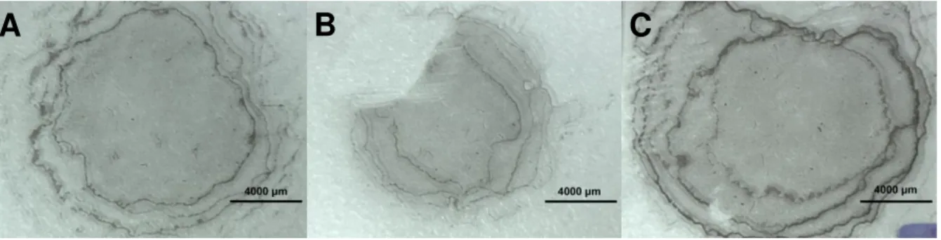
However, since the contacts were deposited by e-beam, which is a very vertical type of deposition, the roughness of the film was able to make the contacts not conductive. The masks for the deposition of contacts have a circle that is used to check the contacts quality. So, one of those circles was used to measure the roughness of the film. The contact used did not have NWs in the middle, and the NWs around the contact were cleaned, to make sure they would not be drafted by the
profilometer’s tip (Figure 4.32).
Figure 4.32 – Graphic showing the profile of an aluminum contact deposited on top of NWs. Inset shows the contact and the direction of the scanning.
The deposition of aluminum reached 100 nm, but it was not constant throughout the circle, and the roughness of the film is clearly excessive.
28
4.2.3.2. Optical characterization
In the electrical characterization of the NWs deposited on interdigitated’s contacts, no correlation between the number of depositions and the resistance was found. However, since there are more NWs deposited after each deposition, the optical properties might change at every deposition. So, five substrates were prepared, each one with an increasing number of passages (Figure 4.33).
Figure 4.33 – Graphic showing the transmittance versus wavelength for all five depositions. Inset show microscopic images from the 5 substrates.
The films demonstrated a good performance overall and quite persistent behavior throughout the solar spectrum.
Figure 4.34 – Graphic showing the transmittance versus wavelength at the visible spectrum for the five depositions. Inset shows the transmittance at 550 nm for all the depositions.