João Ricardo Antunes Afonso
Licenciado em Ciências de Engenharia de Micro e Nanotecnologias
Tuning the electronic properties of
ZnO and CuCrO
2though annealing for
transparent electronic applications
Dissertação para obtenção do Grau de Mestre em Engenharia de Micro e Nanotecnologias
Orientador: Dr. Elvira Maria Correia Fortunato, Prof.
Catedrática, FCT-UNL
Co-orientador: Dr. Renaud Leturcq, Lead R&T
Associate, LIST
Júri:
Presidente: Prof. Doutor Rodrigo Martins Arguente: Prof. Doutor Jonas Deuermeier
Vogal: Prof. Doutora Elvira Fortunato
iii
Tuning the electronic properties of ZnO and CuCrO
2though annealing for transparent electronic applications
Copyright © João Ricardo Antunes Afonso Faculdade de Ciências e Tecnologia
Universidade Nova de Lisboa
v Acknowledgements
It is with great satisfaction that I see the end of my university journey. It was not an easy journey, it had pleasure, laughs, parties but had also lots of difficulties and obstacles along the way, and I happy truly happy with the way things composed during the time and the way I improved as a person during my path to be a Master in Micro and Nanotechnology Engineer.
For this I would like to thank the Institution, Faculdade de Ciências e Tecnologias, specially Departamento de Ciencias dos Materiais and CENIMAT. I would like to thank all the teachers that crossed my path during this journey, mainly to my supervisor Elvira Fortunato, for all the help and for all the effort putting towards the evolution of this course and of the research in Portugal.
I would like to thank my receiving organization LIST, that permitted me to develop my work towards my thesis. It was a fantastic opportunity where I met fantastic person and that permitted me to evolve a lot and discover a completely new working method, the approach of a RTO. I would like to thank Damien Lenoble and Petru Popa, for all the help, support,
supervision and teaching they gave me. Mostly Renaud Leturcq, my supervisor, gave me a fantastic help, in what I found to be a good approach, transmitting a lot of knowledge, helping me giving a direction to my work but giving me the freedom to take decisions, I think this was very important for my satisfaction during this work. All his constant support in harder times needs to be thanked. I would also like to thank the colleagues I found, Nohora, Serena, David, Sabrina, Sunil, Hameeda and Tai, and mainly to my friend Rishabh.
My parents that always supported me, from way before this journey supported in all the possible ways, giving me all the opportunities I could ask for and permitting always that I draw my way and took my personal decisions. To my little sister Beatriz for the relaxing moments.
vii ABSTRACT
Transparent microelectronics applications have been receiving a great amount of research because of the continuous demand for better products from the consumers due to their use in almost every product of the modern-day society. This work comes to explore two of the missing building blocks in completely transparent microelectronics, a capable transparent conductive oxide (TCO) that can substitute indium-tin-oxide (ITO) and a good transparent p-type TCO. The materials studied were ZnO and CuCrO2 that were tuned for a wide range of carrier concentration though changes in deposition parameters and annealing steps. ZnO thin films have shown a wide range of carrier concentration from 8 ∗ 1019approaching 1018 𝑐𝑚−3 and
even values above 1020 𝑐𝑚−3, in the case of Aluminium doped ZnO films. An important
relationship was discovered during this work, a direct interplay of the mobility with the carrier concentration, 𝜇 ∝ 𝑛, that holds in the range between 1018− 3 ∗ 1019𝑐𝑚−3. CuCrO2 thin films
have shown also a wide range of tunability in terms of carrier concentration from 2 ∗ 1021 to
1017 𝑐𝑚−3, showing a progressive increase of optical transmittance from 37% to 60% with the
decrease in carrier concentration, which makes them more suitable for transparent electronics applications. A P-N junction was proposed with these materials with a projected type-II band alignment and optimized carrier concentration of about 5 ∗ 1018 𝑐𝑚−3 on both sides of the
junction. The junction was patterned by etching and photolithography but unfortunately the carrier concentration was not the optimized one, that lead into a ohmic contact.
ix RESUMO
A eletrónica transparente tem recebido uma grande quota da investigação tecnológica, devido à demanda continua por melhores produtos devido à sua utilização em quase todos os produtos do dia-a-dia da sociedade moderna. Este trabalho vem explorar dois dos pontos fundamentais para a evolução desta tecnologia, a substituição do ‘indium-tin-oxide’ (ITO) por outro oxido condutor transparente e a introdução de um bom oxido condutor transparente do tipo p. Os materiais estudados para este efeito foram o ZnO e o CuCrO2 que foram ajustados para uma grande quantidade de concentração de portadores, através de alterações de parâmetros de deposição e de processos de recozimento. Os filmes de ZnO mostraram um amplo alcance de concentração de portadores desde 8 ∗ 1019até 1018 𝑐𝑚−3, e até valores acima de 1020 𝑐𝑚−3,
no caso dosfilmes dopados de Aluminio. Uma relação importante descoberta durante este trabalho foi a relação direta entre a mobilidade e a concentração de portadores, 𝜇 ∝ 𝑛, que se manifestou entre 1018− 3 ∗ 1019𝑐𝑚−3. Filmes finos de CuCrO2 mostraram também um
grande alcance em termos de concentração de portadores desde 2 ∗ 1021 até 1017 𝑐𝑚−3,
mostrando um aumento progressivo da transmitância ótica desde 37% até 60% com a diminuição na concentração de portadores o que torna os filmes mais aplicáveis à eletrónica transparente. Uma junção P-N foi proposta com estes materiais com um alinhamento de banda tipo-II projetada e otimizado para uma concentração de portadores de 5 ∗ 1018 𝑐𝑚−3, em ambos
os lados da junção. A junção foi padronizada por etching e fotolitografia, mas infelizmente a concentração de portadores utilizada não foi a otimizada o que induziu um contacto óhmico.
xi
Abbreviation List
ALD – Atomic Layer Deposition AZO – Aluminium doped zinc oxide CVD – Chemical Vapour Deposition FTO – Fluorine Tin Oxide
GGA - Generalized Gradient Approximation ITO – Indium Tin Oxide
LED – Light Emitting Diode
KPFM – Kevin Probe Force Microscopy
MOCVD – Metal Organic Chemical Vapour Deposition
MOSFETS - Metal Oxide Semiconductor Field Effect Transistor PBE – Population Balance Equation
PL – Photoluminescence
SEM – Scanning Electron Microscopy TFT – Thin Film Transistor
TCM – Transparent Conductive Material TCO – Transparent Conductive Oxide UV- Ultraviolet
VB – Valence Band
xiii
Symbols List
e - Electron charge I – Current
ION – Current when diode is in ON state IOFF – Current when diode is in OFF state n – Ideality factor
k – Boltzmann constant s – Second
V – Electrical Potential T – Temperature
𝜎
- Conductivity
µ - electron mobilityxv
Table of Contents
1 Motivation and Objectives ... 1
2 Introduction ... 2
2.1 - Zinc Oxide ... 2
2.2 - Copper Chromium Oxide ... 3
2.3 - Annealing of TCOs ... 4
2.4 - Transparent P-N junction ... 6
3 Materials and Methods ... 7
4 Results and Discussion ... 10
4.1 ZnO ... 10
4.1.1 ALD deposition temperature study ... 10
4.1.2 Influence of annealing temperature, atmosphere and time on mobility and carrier concentration ... 11
4.1.3 XRD ... 16
4.1.4 SEM ... 17
4.1.5 Photoluminescence ... 18
4.1.6 Conclusion ... 19
4.2 CuCrO2 ... 20
4.2.1 As-deposited electrical properties ... 20
4.2.2 Annealing processes, influence of Temperature and Time ... 20
4.2.3 Optical Properties ... 23
4.2.4 Conclusion ... 23
4.3 P-N Junction ... 24
4.3.1 Simulation of the p-n junction ... 24
4.3.2 KPFM Results ... 25
4.3.3 Junction Development ... 27
4.3.4 Device Characterization ... 29
5 Conclusion and Future Perspectives... 31
6 Bibliography ... 33
7 Annex ... 37
7.1 Annex 1 – Annealing Conditions and Results ZnO ... 38
7.2 Annex 2 – Seebeck Hall Effect ... 40
7.3 Annex 3 – Annealing Conditions and Results CuCrO2 ... 41
7.4 Annex 4 - Software ... 42
xvii
List of Figures
Figure 1 – Cross-section scheme of the projected P-N junction with a top and bottom contact ... 1
Figure 2 - 2.1- Delafossite structure (a) 3R polytype, R3¯ m space group symmetry (rhombohedral unit cell); (b) 2H polytype, P63/mmc space group symmetry (adapted from Marquardt et al.33); 2.2 - Comparison of the conductivity and the optical transmittance of MOCVD studies developed in J.Crêpellière et al.29 with past literature work with different deposition technique, showing the high conductivity of samples deposited in LIST by MOCVD compared with the past works. ... 4
Figure 3- 3.1 - Resistivity, carrier concentration, and Hall mobility as a function of
annealing temperature for AZO films deposited on SiO2 substrate - adapted from Geng et al. 25; 3.2 - Hall Mobility as function of carrier concentration showing the different scattering regimes, by Minami et al. ... 5 Figure 4 - Plot of the variation of voltage as function of variation of temperature that permits the extraction of Seebeck coefficient and showing the different behaviour between p-type (CuCrO2 deposited at 450ºC) and n-type materials (ZnO deposited at 200ºC) ... 8
Figure 5 - Layout of the mask used with nine patterns with diferent radii, 1000, 500 and 250µm. ... 9
Figure 6 - Photography of the junction with the 2 points used for I-V traces ... 9 Figure 7 - Annealing studies with samples deposited at 200ºC, comparing the influence of the annealing atmosphere on the electrical properties with annealing at 300ºC and 450ºC for 15 and 30 minutes: - a) Carrier Concentration; b) Mobility ... 11
Figure 8 - Annealing with samples deposited at 200°C in order to study the influence of: - a) Annealing temperature on mobility; b) Annealing temperature on carrier concentration; c) Annealing time on mobility; d) Annealing time on carrier concentration ... 12
Figure 9 - Resistivity values resulting of annealing of samples deposited at 130°C as a function of: a) annealing temperature; b) annealing time. ... 12
Figure 10 - Annealing studies of samples deposited at 150°C for 15 minutes: a) Carrier Concentration; b) Mobility as function of annealing temperature ... 13
Figure 11- Resistivity study of samples deposited at 130,150 and 200°C with annealing temperatures ranging from 300° to 450°C and 15 and 30 minutes of annealing time ... 13
Figure 12 – a) Carrier Concentration vs Mobility of all ZnO samples as deposited and annealed. b) Fitting of the Mobility as function of carrier concentration for samples with carrier concentration from 1018 𝑐𝑚 − 3 to 3 ∗ 1019 𝑐𝑚 − 3 ... 14
Figure 13 - Linear fit of ln(carrier concentration) vs annealing time for ZnO samples
deposited at 200ºC and annealed at 450ºC ... 15 Figure 14 - Linear fit of ln(ln(N0)-ln(n)) vs 1000/annealing Temperature with ZnO samples annealed at different temperatures for a fixed time, 900s deposited at 200ºC ... 15
Figure 15 - XRD spectrum of ZnO thin films on θ/2θ configuration normalized to
background ... 16 Figure 16 - XRD calculated Crystallite size on different samples for (100) and (002) planes ... 17
Figure 17 - SEM images of ZnO deposited at 200ºC with a scale of 200nm on a) and 500 nm on b) ... 17
xviii
SEM image with selected spectrum outside the hole; c) Spectrum of elements inside the hole; d) spectrum of elements outside the hole; e) SEM image of the hole with selected study line; f) Elements in the studied line with great presence of Zn, O and Si ... 18
Figure 19 - PL Spectrum with 325nm laser on ZnO thin films: a) Normalized [0, 1] in the UV region; b) original spectrum ... 19
Figure 20- PL spectrum of ZnO thin films: a) with 235nm laser all spectrum normalized; b) with 422nm laser ... 19
Figure 21 - Seebeck Coefficient of CuCrOs samples variation with annealing - a)
Temperature; b) Time... 21 Figure 22- Electrical Properties of CuCrO2 extrapolated using small polaron model variating with annealing conditions: a) Carrier concentration as function of annealing temperature; b) Carrier concentration as function of annealing time; c) Mobility as function of annealing temperature; d) Mobility as function of annealing time ... 22
Figure 23 - Linear fit of ln(ln(N0)-ln(p)) vs 1000/annealing Temperature with CuCrO2 annealed at different temperature for a fixed time, 900s ... 22
Figure 24 - CuCrO2 films - Transmittance in the visible spectrum with samples annealed under different conditions ... 23
Figure 25 - Type-II band alignment schematic adapted from Grundmann et al.49 ... 24 Figure 26- Junction Simulation with carrier concentration on both sides of 5 ∗ 1018 𝑐𝑚 − 3 ... 25
Figure 27 - a) Mapping of surface potential performed by KPFM measurement on ZnO sample '9'; b) Histogram associated with the map of a) ... 25
Figure 28 - Evolution of Difference to HOPG measurements produced by KPFM vs Carrier Concentration of ZnO samples '1' and '9, with an inset energy diagram of the variable position of the Fermi level with different annealing conditions ... 26
Figure 29 - CuCrO2 samples Workfunction difference to HOPG as function of: a)
Annealing Time; b) Carrier Concentration; with an inset energy diagram of the variable position of the Fermi level with different annealing conditions ... 26
Figure 30 - Schematic of the band alignment, showing the type-II alignment with the different Fermi levels depending on the annealing conditions ... 27
Figure 31 - ZnO Film with 135 nm covered with photoresist etched in FeCl2 for 20 seconds, presenting an undercut of 124 nm. ... 28
Figure 32 – a) I-V Curves of different pads in sample 2 with a sweep from -4 to 4 V; b) Conductance (slope from I-V curves) vs pad radius showing the contact size dependence ... 29
Figure 33- SEM image of the junction with a ZnO pad with 250µm radius ... 29 Figure 34 - SEM image of the junction with a ZnO pad with 500µm radius ... 30 Figure 35- SEM image of the junction with the elements present on each side of the
junction, with a) ZnO b) CuCrO2 ... 30 Figure 36- Potential solar cell using ZnO and CuCrO2 as electron transport layer and hole transport layer ... 32
Figure 37- Seebeck measurements curve associated with CuCrO2 as deposited and annealed - a) With changing temperature; b) With changing time ... 40
Figure 38 - Simulated junctions with same carrier concentration on P and N side where is represented the energy levels projection as function of the junction length - a) Carrier
xix
1018𝑐𝑚 − 3and n-side 1018𝑐𝑚 − 3, f) Carrier concentration on p-side 1020𝑐𝑚 − 3and n-side 1019𝑐𝑚 − 3 ... 42
Figure 39 - Junction Optical Images of the junction in sample 2 before – a, b and after the removal of the photoresist – c, d ... 43
Figure 40 - Junction Optical Images of the junction in sample 1 before – a, b and after the removal of the photoresist – c, d ... 44
xxi
List of Tables
Table 1 - State of the art of ZnO annealing atmospheres ... 5 Table 2 - Electrical parameters of ALD deposited ZnO at 130°, 150º and 200°C, with error bars from statistical analysis from 8, 12 and 19 samples respectively. ... 10
Table 3 - XRD analysis with crystallite size of each sample for each peak and the intensity of the given peak ... 16
Table 4 - As-deposited electrical characteristics of CuCrO2 thin films with error bars from statistical analysis of 12 samples ... 20
Table 5 - Bibliography values for defect healing and diffusion ... 23 Table 6 - CuCrO2 thin films as deposited and annealed used for the junction - electrical characteristics, for samples as deposited error is extracted from statistical analysis of the three samples, for the others the Seebeck coefficient error is extracted from the fitting ... 27
Table 7 - ZnO thin films as deposited and annealed deposited on top of CuCrO2 - electrical characteristics ... 28
Table 8 – Annealing Conditions and Electrical Results for ZnO samples deposited at 200ºC ... 38
Table 9 - Annealing plan and electrical results of ZnO samples deposited at 130º and 150ºC ... 39
1
1
Motivation and Objectives
Transparent electronics is one of the technological areas with highest economic importance and still a good development margin, with every year costumers demanding better products, and enterprises and industries trying to overcome their competitors with newer capabilities.
Transparent electronics is used by everyone in displays and sensors in every corner of modern day society. Its further development is however hindered nowadays by two crucial issues. One important piece that is still missing in the material portfolio of transparent conductors is a good transparent p-type transparent conducting oxide (TCO) that could permit full usage of pixels with introduction of fully transparent electronics, the introduction of photovoltaic windows and another panoply of fully transparent applications. The other problem is the expected shortage of Indium, as well as its inflated cost and toxicity, and so the need to find a substitute to the commonly used indium-tin oxide (ITO), that is still the mostly used TCO1.
This work comes with the goal to explore ways to achieve these missing building blocks. The following objectives were investigated during the internship:
Study of ZnO deposited by Atomic Layer Deposition (ALD) as replacement of ITO, and explore the tunability of the films for microelectronics applications through changes in deposition temperature and annealing conditions, with particular attention to the carrier concentration variation and mobility and study the interplay between them.
Study of CuCrO2 deposited by Metal Organic Chemical Vapour Deposition (MOCVD) in the group as p-type TCO, and study ways to tune the carrier
concentration and to increase the optical transmittance of these films, to be suitable for several microelectronics applications.
Development of a vertical P-N junction using both the materials such as suggested in Figure 1, with a top and a bottom contact. The patterning of the junction will be processed with optical lithography and wet etching. For this junction, the important challenge of n-type and p-type TCOs is to obtain a reduced carrier concentration while keeping a high mobility on both sides in order to optimize the rectification properties.
Completely transparent P-N junctions would permit the introduction of energy harvester windows, development of good UV emitters and detectors and transparent CMOS transistors enabling the use of full pixels in displays.
2
2
Introduction
TCO layers have been one of the biggest research focus in the recent years, due to their wide use in optoelectronic devices, from transparent electrodes in displays to Light Emitting Diodes (LEDs) or photovoltaic cells. TCOs are a special kind of materials that combine high electrical conductivity and large optical bandgap1,2. The extensive research is focused on finding a substitute to ITO as well as overpassing the lack of a good p-type TCO, that would enable the building of a transparent P-N junction1. Here we investigate in more details two potential candidates, ZnO as a replacement of ITO, and CuCrO2 as p-type TCO.
2.1
- Zinc Oxide
ZnO is a direct bandgap semiconductor (Eg=3.3eV) with a large exciton binding energy (60meV) at room temperature 1,3–5. The most common structure of ZnO is the wurtzite hexagonal structure6. ZnO films have received particular attention because of good electrical and optical properties (transmittance above 80% in the visible region 7), high electrochemical stability, good resistance against Hydrogen plasma and low fabrication cost compared with indium-tin-oxide (ITO), placing it as a great candidate for industrial applications 3,5,8.
ZnO has been studied in diverse structures and with several different deposition techniques, as detailed by Ozgur et al.9. These films can be used for several applications from transparent electrodes (in particular for Aluminium doped Zinc oxide (AZO) films) , light emitting diodes, solar cells, gas sensors and bulk acoustic wave devices or transparent conductive coatings 2,5,6,8.
The wurtzite structure of ZnO is favoured by a (002) crystal orientation in most of high temperature techniques. This is because (002) orientation has the highest atomic packing density and the minimum surface free energy. Therefore the c-axis orientation is the most
thermodynamically favourable growth of ZnO structure10. The crystal orientation can be important when it is used as nanostructures, such as vertically aligned nanowires10–12.
In order to have thin films that can supply micro and nanoelectronics, with precise control of film thickness, conformality and morphology while keeping compatibility with low
temperatures (less than 200ºC) for transparent and flexible electronics, Atomic Layer Deposition (ALD) as an interesting candidate. A binary introduction of fluxes separated by a purge step permits layer-by-layer control of deposition through self-limiting surface
reactions5,13. Deposition temperature4,14, purging time15 and introduction of dopants2,5,16 have been shown to modify the films properties. Electrical characteristics show an increase in resistivity with the decrease of deposition temperature 4,16. At deposition temperature below 100ºC, the films have less preferential orientation and are more amorphous than the films deposited at higher temperatures, which show polycrystalline films with preferential
orientations on (100), (002) and (101) planes13,14,17. Concerning the optical properties, lower deposition temperature films show higher transmittance in the visible region 14. This allows ALD deposited films to have a wide variation of properties depending on the chosen conditions, what makes ALD a very interesting solution for deposition of thin-films. For thicker films the small growth rate (typically 0.18-0.20 nm/cycle for ZnO 18) is a very limitative factor.
Functional properties of ZnO are determined in great part by the inclusion of intrinsic defects during the growth process. These defects contribute mainly to the electrical and
3
supported by Kevin Probe Force Microscopy (KPFM) measurements and that these measurements can give an important information about the doping profile22.
ZnO films present a strong ultraviolet emission that can be applied for optoelectronics, ZnO usually has two photoluminescence (PL) peaks centred in green (2,38eV) and in Ultraviolet (3,18eV). The green peak is assumed to be caused by the intrinsic defects presented before.23–25 It is believed that the increase of green peak is related to increase of zinc interstitials and oxygen vacancies. The ultraviolet (UV) emission peak corresponds to the exciton transition.23,24
In order to improve the electrical properties to be able to compete as a transparent conductive oxide (TCO) with ITO, ZnO has been doped with group-III elements11,25,26, among them Al-doped ZnO films show great potential as TCO and for transparent electrode purposes with high mobility and very low resistivity. Several studies point out for a maximum mobility as well as maximum optical transmittance films at 3 at. %5,26. For thin films with higher Al
concentration it is shown a strong decrease of the conductivity as well as an abrupt increase of the optical bandgap, that can be justified by the appearance of Al2O3 phase 5,27. Therefore, AZO and ZnO films can play a significant role substituting ITO as the main n-type TCO as well as fulfilling many other roles in optoelectronics as a semiconductor layer.
2.2
- Copper Chromium Oxide
A tremendous amount of research has been applied with efforts focusing on finding a p-type material with properties matching the widely used n-type TCOs. , AMO2 (with A = Cu or Ag and M = Al, Sc, Cr, Fe, Ga, or Y) with the delafossite structure, have received a lot of focus on research as a potential TCO, with very promising electrical and optical properties. Still these materials are running orders of magnitude behind in terms of conductivity when compared with n-type TCOs28,29. The highest conductivity of 220 S.cm-1 was reached for Mg doped CuCrO
230, although this value is not confirmed by further studies. Special attention has been given to CuMO2 materials due to their expected large hole mobility resulting from the interaction of Cu 3d states with O 2p states, similar to the interaction in Cu2O where the valence band is
dominated by Cu 3d states 28,31. Cu
2O has a narrow bandgap (2,17eV) while CuMO2 materials present a much wider bandgap (above 3eV) by introduction of this large radius metal while keeping the high conductivity28–32.
In the delafossite each Cu atom is coordinated with two oxygen atoms, forming O-Cu-O dumbbells parallel to the c axis. Oxygens are coordinated with three MIII atoms as shown in Figure 2which can lead to two structures, a rhombohedral (Figure 2.1 a)) or hexagonal (Figure 2.1-b)) unit cell 32,33. In this material, the hole conduction is believed to be through small polaron hopping mechanism. Although Cu-based delafossites have shown high mobility values for p-type semiconductors (up to 1 cm2 V-1 s-1) 31,34–36, it is complicated to increase these mobility values with this conduction mechanism35.
Copper chromium oxides have advantages compared to other delafossites in terms of high density of states of 3d M cations originated by Cr3+ near the valence band maximum permitting good hole mobility, covalent mixing between oxygen and chromium ions and good dopability, that is most efficient with Mg, Fe, N2 or Zn that allow great conductivity increase. These advantages make CuCrO2 a perfect candidate for p-type TCOs29,32. Still it is to notice that compared with CuAlO2 it usually presents lower transmittance37. Mg is the most common way of doping CuCrO2, and as shown by Chikoidze et al.38, increasing Mg content will decrease oxygen vacancies and so enhance hole concentration, up to a maximum at 5% Mg. The same work shows an increase in conductivity up to 3 orders of magnitude with Mg concentration of 4.7%. One question still under intense debate regarding the CuCrO2 is the conduction
4
since the change of M cation changes the conductivity by several orders of magnitude, thus showing the importance of this cation in the conduction properties. On the other hand the CuI/CuII states seems to dominate the valence band maximum (VBM) as demonstrated by X-ray photoelectron spectroscopy (XPS) studies39, generalized gradient aproximation (GGA)
calculations39 and population balance equation (PBE) simulations40, thus favoring the Cu hole mechanism39. It is predicted that the increased of the conductivity of delafossite with Cr in the M site is due to the mixing of Cr d states with Oxygen 2p states in the valence band (VB), producing shallower transition level for the Cu-based holes39,40.
There are several methods reported to produce CuCrO2 which include, solid-state reaction41, sol-gel42,43, pulsed laser deposition44, magnetron sputtering45 and CVD46. Usually these
techniques require high temperatures that are incompatible with transparent electronics. A possible solution that was studied by J. Crêpellière et al.29 uses metal organic chemical vapour deposition (MOCVD), to promote the growth of CuCrO2 thin films using direct liquid injection (DLI) CVD in a one step process. This solution allows using temperatures as low as 330˚C, more compatible with transparent electronics. As it is shown in Figure 2.2, it allows large conductivity (up to 17 S cm-1) and lower temperatures at the cost of lower average transmittance in the visible region29. These results show the potential of delafossite CuCrO
2 thin-films when considering the fabrication of transparent P-N junctions particularly suitable for electrical rectification or photodetection purposes.
An intensive study of the deposition characteristics of CuCrO2 by DLI-MOCVD was performed by Lunca Popa et al.28, showing promising values with deposition temperatures of 450ºC presenting conductivities up to 100 S.cm-128 and carrier concentrations of 1021𝑐𝑚−3
without any extrinsic defect doping and with pure phase CuCrO2.
Figure 2 - 2.1- Delafossite structure (a) 3R polytype, R3¯ m space group symmetry (rhombohedral unit cell); (b) 2H polytype, P63/mmc space group symmetry (adapted from Marquardt et al.33); 2.2 - Comparison of the
conductivity and the optical transmittance of MOCVD studies developed in J.Crêpellière et al.29 with past literature work with different deposition technique, showing the high conductivity of samples deposited in LIST by MOCVD compared with the past works.
2.3
- Annealing of TCOs
These materials arise new possibilities not only as a promising candidate in the case of ZnO to become a common TCO, but mostly their combination might permit to create an all-new kind of optoelectronics, enabled by a fully transparent P-N junction.
5
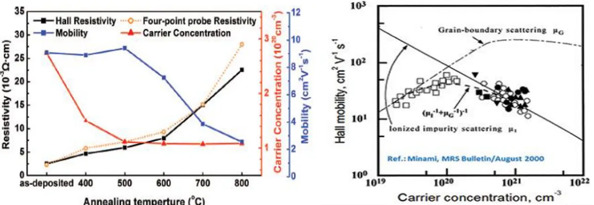
films48, and mostly the electrical properties with a great change in conductivity depending on annealing temperature and time4,25,26. Annealing seems to be an interesting way to control the conductivity, through changes in carrier concentration, and mobility of ZnO making it able to provide the wide range of applications it has been projected for. Figure 3.1 exemplifies this with the variation of mobility and carrier concentration with different annealing temperatures. Literature shows an increase in grain size occurs with annealing temperatures higher than 500ºC. Up to this temperature, the gain size is shown to be kept mostly constant25.
With the potential arise of these capable p-type TCO and in order to produce a good P-N junction one need to study ways to tune the ZnO for lower carrier concentration, but that can conserve the high electron mobility (expected µ = 15 ~ 60 cm2/Vs) 2,5. As shown in literature this can be quite hard to achieve since there appears to be an intrinsic tendency in intrinsic Zinc Oxide to have a decrease of mobility with decrease of carrier concentration 49–51. The mobility of ZnO and doped ZnO films is believed to be dominated by ionized impurity scattering when the carrier concentration is in the range 1020− 1021 𝑐𝑚−3. It thus mainly concerns doped ZnO
films (e.g. AZO). Below this carrier concentration, both the ionized impurity scattering and the grain boundary scattering need to be taken into account.52 According to the past works, there is a peak of mobility that can be found in ZnO close to carrier concentrations of the order of 1020
cm-3, like is seen in Figure 3.2, where grain boundary scattering decreases and is still not overcome by ionized impurity scattering 2,5,47,52.
Figure 3- 3.1 - Resistivity, carrier concentration, and Hall mobility as a function of annealing temperature for AZO films deposited on SiO2 substrate - adapted from Geng et al. 25; 3.2 - Hall Mobility as function of carrier concentration showing the different scattering regimes, by Minami et al.
The annealing atmosphere is still under debate with several works pointing in different directions, and even some of them claiming to have an increase of the conductivity and of the carrier concentration with annealing processes conduced in Vacuum53 and N
254 for ZnO films without extrinsic doping. Still most of works point out to a decreasing carrier concentration in any atmosphere with increasing time and annealing temperature. Table 1 summarize some of the works on the annealing of ZnO with different conditions.
Table 1 - State of the art of ZnO annealing atmospheres
Article Gases Used Considerations
Jin et al.51 Air Decrease in carrier concentration with temperatures from 160-280° - time range from 20 to 120 minutes. Wang et al. 26 Ar, N
2 and Air Two hours annealing at 350ºC. Show better control and less decrease in mobility in Argon annealing. Laube et al. 4 Vacuum and O
6 Lin et al. 55 N
2 Study from 400º to 700ºC showing a major decrease in carrier concentration at 500ºC for 45 minutes.
Kennedy et al. 53 Vacuum and air Carrier density increases in vacuum for 30 min annealing at 500ºC. In air, there is a 4 order of magnitude decrease with same annealing conditions. Geng et al. 25 O
2 Decrease in carrier concentration without big decrease in mobility up to 400ºC. Above this temperature there is a major decrease in mobility.
Lu et al. 54 O
2 and N2 Sequential annealing steps show that N2 leads to a decrease in resistivity and O2 to an increase The optical transmittance of the films seems to be stable under different annealing conditions up to 500ºC 25,26,56.
Like the zinc oxide the delafossite films can also be tuned for the application by thermal annealing, although they require much higher temperature, according to the work of
Götzendörfer et al.37, at least 620ºC are required to measurable difference in electrical
characteristics of delafossite films, what can suggest a higher activation energy of the present defects. Annealing in delafossite above this temperature is shown to reduce the carrier concentration and increase transmittance values in the optical region of 20% 42,45,57, as well as increase of crystallinity and acquisition of pure phase CuCrO2 in case of existence some parasitic phases, such as CuO, CuO2 and CuCr2O429,37,45,57. The evolution of the mobility with post-thermal annealing is not quite understood with measurements from Seebeck coefficient showing a decrease in carrier mobility with any annealing temperature, but then a gradual recovery of mobility with further increase of annealing temperature. Optical bandgap of
delafossite seems not to be affected by annealing processes42. Still in the literature there is a lack of quantitative studies, when it comes to CuCrO2 without extrinsic doping, on the influence of the annealing processes on the electrical properties of the films.
2.4
- Transparent P-N junction
7
3
Materials and Methods
CuCrO2 films were deposited by MOCVD using Direct Liquid Injection - Metal Organic Chemical Vapour Deposition system DLI-MOCVD, (MC200 from Annealsys), which is a stagnation point-flow warm-wall reactor. The used copper and chromium precursors are bis[2,2,6,6-heptanedionato] copper(II) and tris[2,2,6,6- tetramethyl-3,5-heptanedionato]chromium(III), respectively (Cu(thd)2 and Cr(thd)3, Strem Chemicals).
Cyclohexane solutions with a total precursor concentration of [Cu(thd)2] = [Cr(thd)3] = 2,5mM were used. The total canister solution used was 1 L of Cyclohexane with 1.075 g Cu(thd) +1.5 g Cr(thd). The deposition parameters used were: substrate temperature of 450 °C; oxygen flow used was 2000 sccm; nitrogen flow of 850 sccm and the total process pressure was 12 mbar. The process used followed the previous optimization detailed by Lunca Popa et al.28.
ALD deposition of ZnO and Al:ZnO followed the process described by Roge et al.58, using in our case Argon as purge and carrier gas, for 500 cycles and with a pulse sequence:1 -
Diethylzinc (DEZ, Zn(C2H5)2) pulse 150 ms; 2 - purge 10 s; 3 - H2O pulse 200 ms; 4 – purge 10 s. In the case of the AZO at each 30 cycles it was used a pulse of Trimethylaluminum (TMA, Al(CH3)3).
All the annealing processes were performed on a Rapid Thermal Annealing reactor
(Annealsys), at low pressure, using in the case of CuCrO2 films a nitrogen flow of 500 sccm and in the case of ZnO a nitrogen flow of 25 sccm. The annealing curve was first a heating ramp with 5 ºC/s, a waiting time at constant peak temperature and a cooling ramp with -5 ºC/s. The varied annealing time was the waiting time and the heating and cooling times are not counted.
Prior to ALD deposition the glass substrate was previously cleaned in acetone and ethanol and dried with nitrogen jet.
All the measurements were carried out at room temperature.
Electrical measurements were made using Hall effect Measurement Ecopia HMS-3000 with a magnet of 0,562 T using van der Pauw configuration for extracting the carrier concentration and the mobility (in the range between 1 – 107 𝑐𝑚2
𝑉𝑠). The sheet resistance is first measured in
van der Pauw configuration without any magnetic field applied, that permits to calculate the conductivity, and then the Hall voltage is measured with a magnetic field, from which we calculate the carrier concentration. The mobility is extracted as shown in equation 1.
𝜎 = 𝑒(µ
𝑒𝑛 + µ
ℎ𝑝)
(equation 1)In all cases we assume that there is only one type of carriers (majority carriers). We have checked that the majority carriers in ZnO are electrons, and in CuCrO2 majority carriers are holes. We thus neglect the cases where the two carriers can contribute to conductivity, which can potentially result in a miscalculation due to compensation doping.
Mobility measurements are expected to have an error up to 30%, considering an error up to 10% of the 4-Point-Probe measurements and up to 20% in the carrier concentration, coming from a 10% error in the thickness measurement from elipsometry and a 10% error in the Hall resistance measurements.
In addition to the Hall effect measurement, 4-Point-Probe measurements were realized on a Jendel Cylindrical four-point linear probes head with a Keithley Source Meter 2614B to extract the sheet resistance of the films according to equation 2.
𝑅𝑠 = 4.532 ∗ 0.925 ∗𝑉𝐼 (equation 2)
8
reference. In this system, copper blocks are thermally separated one is heated, while the other is kept at room temperature. With this there is a small voltage build-up, this difference in voltage vs. the difference in temperature can be plotted. From the fit of the slope we calculate the Seebeck coefficient, as shown in equation 3. An example of the plot used to extract S is shown in Figure 4,showing the different slopes associated with p and n-type semiconductors.
𝑆 = −∆𝑉∆𝑇 (equation 3)
Photoluminescence measurements were realized on a Renishaw inVia microspectrometer using a grating of 300 gr/nm, an objective of 15 times UV (Thalabs) and with laser power of 100% corresponding to 8mW and using two lasers a UV and blue one with corresponding 325nm and 442nm wavelength. Transmission and reflectance spectrum were acquired in the range from 1500 to 250nm using a Perkin Elmer LAMBDA 950 UV/Vis/NIR
Spectrophotometer with a 150 mm InGaAs Integrating Sphere.
Figure 4 - Plot of the variation of voltage as function of variation of temperature that permits the extraction of Seebeck coefficient and showing the different behaviour between p-type (CuCrO2 deposited at 450ºC) and n-type
materials (ZnO deposited at 200ºC)
The structure of the grown films was studied by X-Ray Diffraction (XRD), Bruker D8 Discover, using monochromatic Cu Ka radiation (l = 1.54 Å) at 40 kV and 40 mA. The analyses were performed using the θ/2θ configuration from 25 to 50º at a scanning step of 0.02º and with 3s/step. Kevin Probe Force Microscopy (KPFM) measurements have been performed on a Bruker Innova using the surface potential mode as amplitude modulation. Surface topography is obtained in the first pass and the surface potential is measured on the second pass. Freshly cleaved highly-oriented pyrolitic graphite (HOPG) is used as reference. The measurements are performed under dry N2 atmosphere to avoid contaminations on the surface. The surface morphology of the films was inspected by Scanning Electron Microscopy (SEM) with 10kV of acceleration voltage, FEI Helios Nanolab 650 with EDX spectrum analysis connected to SEM Oxford Instrument Xmax 50mm2 with the previous acceleration voltage. Thickness of the CuCrO2 films was measured using the same equipment with a cross-section view on silicon.
The thickness of the ZnO films was measured on a Si wafer beneath the samples using ellipsometry M2000J.A. Woollam Co with a Si + Native SiO2 + ZnO model.
Dry etching was processed on PLASMATHERM 790 Reactive Ion Etching chamber using CF4+Ar gases and with 500W RF Power. It was used a bi-layer of LOR3A with 300 nm and on top a Shipley S1813 with 1.2 µm, spin-coated for 1 minute at 4000 rpm and with an acceleration of 1000 𝑟𝑝𝑚
9
single layer of ShipleyS1813 with the previous conditions. It was used on both etching cases HDMS as a promotion adhesion that was spin-coated at 4000 rpm for 30 seconds with an acceleration of 1000 𝑟𝑝𝑚
𝑠2 , baked for 1 minute for 115ºC.
The lithography was processed on a Heidelberg Instruments MLA 150 with the pattern shown in Figure 5, with circular patterns with 3 different radii, 250, 500 and 1000 µm. It was run a dose test and used 90 𝑚𝐽
𝑐𝑚2. After exposure, the samples were developed using a MF319 for
40 seconds and after rinsed for 30 seconds. The samples were dipped in FeCl2 where several solutions were tried favouring the used one at 0.1% for 15 seconds. The samples were then cleaned in acetone for 2 minutes for photoresist removal. The images of the samples were taken using Leica DFC295 microscope.
For electrical characterization of the junction was used a configuration with 2 points at different voltage, with a voltage sweep and measuring the current between the two tungsten tips, as shown in Figure 6. The Sweep tip was kept on the CuCrO2 contacted with silver paste and the constant -0 V was kept on ZnO pads.
Figure 5 - Layout of the mask used with nine patterns with diferent radii, 1000, 500 and 250µm.
10
4
Results and Discussion
4.1
ZnO
The Study of the ZnO was proposed with the objective of studying the influence of the deposition temperature on the carrier concentration and study ways to further decrease this carrier concentration for transparent microelectronics applications while keeping a high mobility. The relationship between the mobility and the carrier concentration was more particularly studied. For this purpose, we performed three depositions by ALD at different temperatures. These films were consequently annealed studying the influence of the
atmosphere, the time and the temperature. XRD tests were run to study the crystallite size and SEM to confirm the morphology. PL was studied to see the impact of the annealing on the excitonic peak.
4.1.1
ALD deposition temperature study
Table 2 - Electrical parameters of ALD deposited ZnO at 130°, 150º and 200°C, with error bars from statistical analysis from 8, 12 and 19 samples respectively.
The deposition temperature plays a significant role in the electrical properties of the films, as shown in Table 2. In the chosen temperature range, the growth rate by ALD is expected not to be independent on this temperature window4,18. However, while all three depositions were performed with the same 500 cycles, the thickness of the deposition at 150°C is bigger than the other two depositions. The main reason is a different configuration in the reactor being used for this particular deposition. On the other hand, almost no difference is seen between the
depositions at 130 and 200°C, with a growth per cycle of 2 Å/cycle, in the expected ALD growth rate of 1.8-2.0 Å/cycle18. The most important result is the decrease in carrier concentration, in mobility and consequently decrease in conductivity of the films with the decrease in the deposition temperature. We further note that, under these conditions, the carrier concentration is still too high for use in active electrics applications. For this reason, we further studied an annealing step in order to decrease it.
AZO films were also deposited. The deposition was processed at 200ºC and resulted in films with a thickness of 84 nm, with an average carrier concentration of 4 ∗ 1020 𝑐𝑚−3, and mobility
Deposition
Temperature
130
°
C
150
°
C
200
°
C
Carrier
Concentration
(cm
-3)
2.7 ∗ 1019
± 6 ∗ 1018 5.1 ∗ 10
19
± 5 ∗ 1018 7.7 ∗ 10
19
± 8 ∗ 1018
Mobility
(cm
2/Vs)
16.4 ± 2.6 18 ± 0.9 22.6 ± 2.5Conductivity
(S/cm)
62.2 ± 12.8 126 ± 3.42 166 ± 47.911
of 12𝑐𝑚𝑉𝑠2. These films are expected to have 3% Al content. Since AZO is intended for metallic-type transparent contacts, no further annealing was planned for this material.
4.1.2
Influence of annealing temperature, atmosphere and time on mobility and
carrier concentration
Firstly, it was programmed an annealing with the 200°C deposited samples based on previous literature works, to have a deeper understanding of the influence of temperature, ranging from 300° to 450°C, atmosphere, using N2 and argon during the annealing process and varying the time between 15 and 360 minutes. In annex 1 is presented the table with the electrical results and annealing plan of every sample.
In Figure 7is presented the influence of the annealing atmosphere on the electrical
properties: carrier concentration and electron mobility. It is possible to see the little influence on the electrical proprieties with the change in atmosphere between N2 and Ar, with these slight changes falling in the associated error considerer for Hall effect measurements. With these conclusion, all annealing tests were further studied under N2 atmosphere.
Figure 7 - Annealing studies with samples deposited at 200ºC, comparing the influence of the annealing atmosphere on the electrical properties with annealing at 300ºC and 450ºC for 15 and 30 minutes: - a) Carrier Concentration; b) Mobility
As shown in graphic 8. we see that the temperature has a strong influence over the carrier concentration with a severe decrease of the mobility. Annealing steps processed at 300ºC show very little impact on the initial values and with increasing temperature is shown a big decrease in carrier concentration. This suggests that the annealing temperature required for starting to heal defects on these samples deposited at 200ºC is above 300ºC, since with 350ºC there is already a factor of 4 times reduction in carrier concentration. The highest annealing temperature was 450ºC, to avoid changes in the crystalline structure of the ZnO, with this annealing showing a 10 times decrease when compared with the as-deposited samples, with 15 minutes annealing. The mobility is always impacted in a similar way showing a gradual decrease comparable with the decrease in the carrier concentration. The annealing time was seen to have much smaller impact in carrier concentration, with times from 15 min (8.6 ∗ 1018 𝑐𝑚−3) to 6 hours
(3.8 ∗ 1018 𝑐𝑚−3) being studied. This 24 times increase in time resulted in a decrease in carrier
concentration to about half the original value and a similar decrease in mobility. These samples presented a carrier concentration from 8 ∗ 1019 cm−3 as-deposited and with 300ºC annealing to
a minimum of 3 ∗ 1018 cm−3 with annealings at 450ºC for 6 hours. The mobility of the films
decreases from 26 to 2𝑐𝑚2
12
It was studied another annealing plan for the samples deposited at 130° and 150°C, to further decrease the carrier concentration, in this case with samples deposited at another temperature.
Figure 8 - Annealing with samples deposited at 200°C in order to study the influence of: - a) Annealing temperature on mobility; b) Annealing temperature on carrier concentration; c) Annealing time on mobility; d) Annealing time on carrier concentration
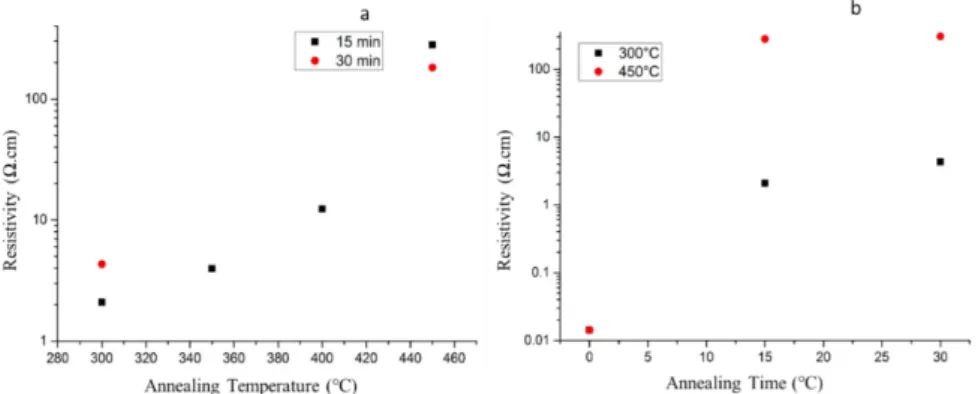
The samples with deposition temperature of 130°C presented after annealing very low carrier concentration and mobility values, what was a problem to be measured by this Hall-Effect system with accuracy, due to the range of mobility going only as low as 1𝑐𝑚2
𝑉𝑠. The
values of carrier concentration and mobility can thus not be extracted accurately using our system, and is preferred to analyse the resistivity measured by 4-Point-Probe. The resistivity change as a function of annealing temperature and annealing time are shown in Figure 9. Still it is possible to observe once again the strong increase of resistivity with the increase of annealing temperature and a small increase also in resistivity with the increase in time
Figure 9 - Resistivity values resulting of annealing of samples deposited at 130°C as a function of: a) annealing temperature; b) annealing time.
13
annealing for 30 minutes. These samples have shown a wide range of tunability of carrier concentration from 2.6 ∗ 1019𝑐𝑚−3 to values approaching 1018 𝑐𝑚−3 as represented in Figure
10. Once again it is possible to associate a decrease both in carrier concentration and in mobility for the samples that were possible to measure with accuracy (annealing steps up to 350ºC).
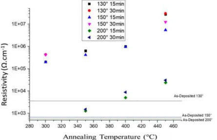
To a bigger extend it is possible to associate the increase in resistivity with both the increase in temperature and in time as shown in Figure 11. Figure 12 represents all the samples annealed between 300 and 450ºC, it is presented with resistivity in order to compare samples with lower carrier concentration and mobility and in order to compare films with different thicknesses. We clearly evidence the increase of resistance of the films with the increase in annealing
temperature, but also the low influence of the time in most of the cases. It is also shown that any annealing temperature above the deposition temperature on the samples deposited at 130ºC and 150ºC show a significant decrease in the carrier concentration leaving a big gap where it is hard to tune it precisely.
Figure 10 - Annealing studies of samples deposited at 150°C for 15 minutes: a) Carrier Concentration; b) Mobility as function of annealing temperature
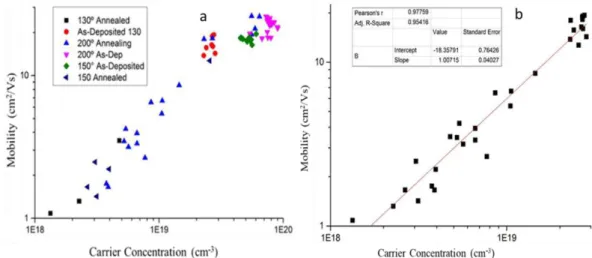
Still as an overall between all the deposition temperatures and annealing performed it is possible to achieve any carrier concentration from below 1 ∗ 1018 𝑐𝑚−3 to 8 ∗ 1019 𝑐𝑚−3, as
shown by Figure 13-a). Also in this graphic, we clearly observe a scaling low between the carrier concentration and the mobility. A fit of the data below the carrier density of 3*1019 cm-3 shows a linear relationship, 𝜇 ∝ 𝑛, as shown in the fitting made in Figure 13-b).
14
This scaling law is a major result that allows us to understand why the decrease in the carrier concentration by the effect of thermal annealing is always impacting the mobility. This is associated with the close relationship that they have due to the type of scattering mechanism never changes, what can be confirmed by XRD, to evaluate the difference in grain boundaries with annealing.
Figure 12 – a) Carrier Concentration vs Mobility of all ZnO samples as deposited and annealed. b) Fitting of the Mobility as function of carrier concentration for samples with carrier concentration from 1018 𝑐𝑚−3 to 3 ∗ 1019 𝑐𝑚−3
From Figure 13-a) there are two main regimes, a first regime where there is a linear increase of the mobility with the increase in carrier concentration, that is explored in Figure 13-b) with the fitting, and another regime above 3 ∗ 1019 𝑐𝑚−3 where there is a saturation of the mobility
with the increase in carrier concentration. The first regime can be associated with the expected increase of mobility with the increase of the Fermi level for the grain boundaries scattering mechanism. Still with a further increase of carrier concentration, there starts to be an interplay between the grain boundary scattering and the ionized impurity scattering. The latest has an expected decrease of mobility with the increase in carrier concentration, what creates a region where mobility is stable for a small range of carrier concentration. This is in accord with previous works such as Minami et al. 52. AZO films present a higher carrier concentration, 4 ∗
1020 𝑐𝑚−3 and follow this trend with a decreased mobility, 12 𝑐𝑚2/𝑉𝑠 as compared with the
as-deposited ZnO thin films.
With the considerations made for the annealing time and temperature study, a model was proposed that could explain the carrier concentration behaviour of the films with different annealing steps.
Assuming that the kinetics of the chemical reaction corresponding to the annealing of doping defects is of first order, the electron concentration, n can be expressed as a function of annealing time, t in a general way as:
𝑛(𝑡) ≈ 𝑁𝑑(𝑡) = 𝑁0𝑒−𝑘𝑡+ 𝑁𝑟𝑒𝑠 (equation 4)
where Nd is the donor dopant concentration, Nres is the residual acceptor concentration after infinite annealing, N0+Nres is the initial carrier concentration (as deposited) and k is the rate constant.
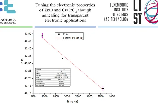
We first check that the assumption of a first order kinetics is valid by fitting ln(n) vs. t for
15
Figure 13 - Linear fit of ln(carrier concentration) vs annealing time for ZnO samples deposited at 200ºC and annealed at 450ºC
Assuming that the reaction is simply activated, the rate constant k can be expressed as a function of the annealing temperature T using an activation energy Ea:
𝑘(𝑇) = 𝐴𝑒− 𝑘𝐵𝑇𝐸𝑎 (equation 5) where A is a constant and kB is the Boltzman constant.
Relating equations (4) and (5), we can express the carrier concentration as a function of annealing temperature T and annealing time t:
𝑛(𝑇, 𝑡) = 𝑁0exp (−𝐴𝑡 exp (−𝑘𝐸𝐵𝑎𝑇)) + 𝑁𝑟𝑒𝑠 (equation 6)
In our case we can neglect in the fit the residual dopant concentration. In this case the relationship can be written:
ln(ln 𝑁0− ln 𝑛(𝑇, 𝑡)) = ln(𝐴𝑡) −𝑘𝐸𝐵𝑎𝑇(equation 7)
Taking the “as deposited” carrier concentration as initial dopant concentration N0 =
7.8 ∗ 1019cm-3, we can plot ln(ln 𝑁
0− ln 𝑛(𝑇, 𝑡)) at fixed annealing time t = 900 s as a
function of 1/T.
Figure 14 - Linear fit of ln(ln(N0)-ln(n)) vs 1000/annealing Temperature with ZnO samples annealed at different temperatures for a fixed time, 900s deposited at 200ºC
The data fit well with the activation energy model, and we obtain Ea/kB = 3550 ± 100 K,
16
4.1.3
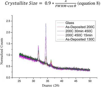
XRD
In order to explain the scaling behaviour between the mobility and the carrier density, we have assumed that the scattering mechanism due to grain boundaries does not change with annealing. In order to confirm this assumption, we have used XRD in order to estimate the crystallite size. Figure 16 represents a θ/2θ XRD spectrum of some of representative ZnO thin films. It is possible to see the peaks corresponding to the crystal orientations (100), (002) and (101), the most commonly ones associated with ZnO thin films. The main observation is the relative increase of the intensity of (002) peak on the samples deposited at 200ºC and annealed at 450ºC.
The lower boundary of crystallite size was studied from the FWHM extracted with the software ‘intensity’ and calculated with Scherrer equation (equation 8), where λ is the X-Ray wavelength, that in this case is 0,15 nm. The shape factor was assumed to be 0.9, a
simplification made assuming the shape of the nanoparticles would be approximately spherical. 𝐶𝑟𝑦𝑠𝑡𝑎𝑙𝑙𝑖𝑡𝑒 𝑆𝑖𝑧𝑒 = 0.9 ∗𝐹𝑊𝐻𝑀∗𝑐𝑜𝑠 𝜃𝜆 (equation 8)
Figure 15 - XRD spectrum of ZnO thin films on θ/2θ configuration normalized to background
Table 3 - XRD analysis with crystallite size of each sample for each peak and the intensity of the given peak
Crystallite Size(nm)
Sample (100) (002) (101) (100) Peak Intensity
(002) Peak Intensity
(101) Peak Intensity
200C - As Dep 25.97 26.83 26.83 83 64 30
130C - As-Dep 24.39 21.18 20.12 85 65 29
200C - 450C 30 min 26.83 25.97 19.17 143 425 26
200C - 450C 15 min 25.97 24.39 17.89 142 265 27
17
any significant change and mainly without a tendency of decrease of grain boundary when there is a decrease in carrier concentration, one can claim that the decrease in carrier concentration is most likely due to healing of defects during the annealing process and the decrease in mobility is associated with this decrease in carrier concentration and not in the increase of grain
boundary in the film.
Figure 16 - XRD calculated Crystallite size on different samples for (100) and (002) planes
4.1.4
SEM
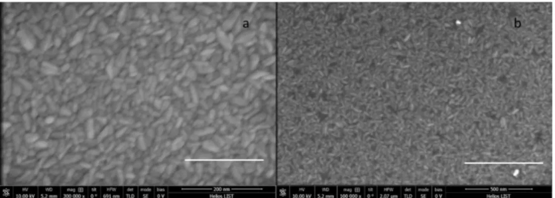
SEM analysis was proceeded on several samples deposited at 130°, 150° and 200° without any annealing, deposited at 200° annealed at 450° for 30 minutes and deposited at 130°
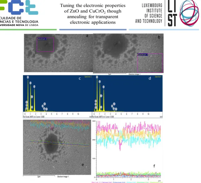
annealed at 300° and 350° for 15 minutes. The observed morphology was similar in all samples with a nanorods/nanoneedles morphology, as shown in Fig. 18. The estimation of size can confirm the average crystallite size calculated by XRD. It was seen in all samples holes, that were studied by EDX as shown in Figure 19. We can see that inside the hole there is no additional element. With a line studying the distribution of this elements like shown in Figure 19 f), it is possible to observe that inside the hole there is a decrease in Zinc, what suggests that it is just a vacant space where there is no Zinc Oxide. This was most likely caused by the cleaning procedure using acetone and ethanol that left some residues after evaporation, thus leaving a non-deposited zone. Unfortunately, this was noticed quite late and was not possible to re-do all the experiments for having a more uniform deposition. Still this lack of Zinc Oxide will only influence the results, mainly the mobility and conductivity, in a negative way, lowering them, what can suggest that without these holes formation electrical results could be even better.
18
Figure 18 - SEM/EDX imaging and element mapping of ZnO sample deposited at 130°C and annealed at 300° for 15 minutes - a) SEM image with selected spectrum inside the hole; b) SEM image with selected spectrum outside the hole; c) Spectrum of elements inside the hole; d) spectrum of elements outside the hole; e) SEM image of the hole with selected study line; f) Elements in the studied line with great presence of Zn, O and Si
4.1.5
Photoluminescence
19
Figure 19 - PL Spectrum with 325nm laser on ZnO thin films: a) Normalized [0, 1] in the UV region; b) original spectrum
The blue laser could give an important information about the defects peak but, due to the deposition of the samples being carried on glass, peaks originating from the substrate are overlapping with the expected ones for the defects. We could thus not analyse the evolution of the peaks related to the defects with annealing steps.
Figure 20- PL spectrum of ZnO thin films: a) with 235nm laser all spectrum normalized; b) with 422nm laser
4.1.6
Conclusion
As a conclusion for the ZnO deposition and annealing for the tunability of the carrier concentration and mobility, it is possible to observe a tunability of the films for a wide range of carrier concentration. Increasing deposition temperature has shown an increase in carrier concentration and in mobility. For the annealing, it was observed a negligible effect of the atmosphere, that can be justified from the fact that both gases used are inert and there is no insertion of dopants but instead only the reorganization and healing of intrinsic point defects. It was noticed the big impact with the temperature and a smaller impact in the annealing time. This can be justified with the fact that the selected times were higher than the relaxation time, what in the logarithmic decrease expected for an activated behaviour means that the influence of a further increase in time will have a rather small effect. Most likely in this case the smallest annealing time used, 900 seconds is already much larger than the relaxation time. Increasing the annealing temperature increases the resistivity, which can be associated with a decrease in carrier concentration and mobility. The observed decrease of the carrier concentration with annealing is always associated with a decrease of the mobility as shown in Figure 13. These interplay is present from carrier concentration of 1018 𝑐𝑚−3 to 3 ∗ 1019 𝑐𝑚−3, where we find a
20
1021 𝑐𝑚−3, and it was verified a new decrease in mobility with an increase in carrier
concentration. The PL analysis show a red shift with decreasing carrier concentration but failed to show a tendency of the defects peaks with changing annealing conditions due to the substrate overlapping its expected peaks.
This work shows that, in order to keep high mobility and try to further decrease carrier concentration, other solutions need to be found, such as changing the deposition parameters.
4.2
CuCrO2
Delafossite films deposited by MOCVD were studied with two kinds of annealing steps, varying the temperature from 650ºC to 850ºC for a fixed time, 15 minutes and keeping the temperature constant at 900ºC and changing the time from 1 to 4000 seconds. It was measured the Seebeck coefficient to make possible the extraction of the carrier concentration using small polaron model. The optical transmittance of the films with different annealing temperatures was analysed.
4.2.1
As-deposited electrical properties
Two sets of CuCrO2 were deposited on 2” sapphire wafers by MOCVD, with similar growth conditions and similar electrical properties. The wafer was cut in approximately 1x1cm squares and in every sample, was measured the conductivity, by four-point-probe and Seebeck
coefficient.
Table 4 - As-deposited electrical characteristics of CuCrO2 thin films with error bars from statistical analysis of 12 samples
Conductivity
(
𝑆𝑐𝑚
)
Seebeck
Coefficient (
𝜇𝐾𝑉
)
Carrier
Concentration
𝑐𝑚−3CuCrO
2As-Deposited
20 ± 8.2 104 ± 7 1.6 ∗ 1021 ± 2 ∗ 1020The sample’s thickness was measured by SEM cross-section with values of 200 ± 40 𝑛𝑚. It is to notice that this process still lacks homogeneity in the same wafer there are still very noticeable differences. The Seebeck Coefficient values were negative as expected confirming the p-type behaviour of the films. Hall mobility measurements were not possible in this
material, since the mobility was too low, so as an alternative carrier concentration was estimated from the Seebeck Coefficient. The small polaron model was used based on previous literature and works realized by the group28,29. Using equation 9, where the density of copper sites in stoichiometric CuCrO2 considering the theoretical lattice is
2.3 ∗ 10
22, and S is the Seebeck
coefficient,
considering the main mechanism of conduction as being the Cu+/Cu2+60. The calculated as deposited mobility was 0.08 cm2/Vs.𝑝 =
11+4 exp(𝑆∗𝐾𝑏𝑒)
∗ 2.3 ∗ 10
22 (equation 9)
4.2.2
Annealing processes, influence of Temperature and Time
21
studied at a constant temperature 900ºC, and with times ranging from 1 to 4000 seconds. Temperatures above 900ºC were not studied to keep safely bellow the stability limit of Copper delafossite materials that are pointed by previous works to be 1100ºC 60.
For the sample annealed at 900ºC for 4000 seconds, it was not possible to measure the conductivity and the Seebeck coefficient given the instruments range. The Seebeck values annealing annealing prove the p-type conductivity of every film as shown in annex 4. The increasing temperature as well as the increasing time show a major decrease in the film carrier concentration with a film tunability from 1021− 1017𝑐𝑚−3, over 4 orders of magnitude. The
increasing temperature shows a slow decrease in the carrier concentration and more controllable, but for industry processes flash annealing steps at 900°C can be an important solution. In Figure 23 c) and d) the mobility decrease is obvious with any annealing, but a phenomenon occurs in both cases, that after a big decrease, at 700°C and with 30 seconds, the increasing annealing temperature and time does not further decrease the mobility, but instead there is a small recovery. This can prove to be of major importance since the film mobility is rather low and further decreases might prevent to achieve a minor carrier concentration suitable for the electronics applications. Opposite to temperature that the increase in the temperature always cause a bigger decrease in the carrier concentration, in case of time a further increase of time after 200 seconds seems to cause a very small decrease in carrier concentration. This can be explained by the fact that 200 seconds is already larger than the typical relaxation time, and can suggest that this time will be enough for healing of most defects at a given temperature. A further time study with more intermediate points should be done, in order to see the evolution behaviour between 2 and 200 seconds.
22
Figure 22- Electrical Properties of CuCrO2 extrapolated using small polaron model variating with annealing conditions: a) Carrier concentration as function of annealing temperature; b) Carrier concentration as function of annealing time; c) Mobility as function of annealing temperature; d) Mobility as function of annealing time
With the considerations made for the annealing time and temperature study, a model was proposed that could explain the carrier concentration behaviour of the films with different annealing steps. The assumed model was the same as the one proposed for the ZnO (see section 4.1.2), reminded in equation 10.
ln(ln 𝑁0− ln 𝑝(𝑇, 𝑡)) = ln(𝐴𝑡) −𝑘𝐸𝐵𝑎𝑇 equation 10
The calculated time constant at 900ºC, was k = 0.040 0.005 s-1. Taking the “as deposited”
carrier concentration as initial dopant concentration N0 = 1.6 ∗ 1021cm-3, we can plot
ln(ln 𝑁0− ln 𝑝(𝑇, 𝑡)) at fixed annealing time t = 900 s as a function of 1/T.
Figure 23 - Linear fit of ln(ln(N0)-ln(p)) vs 1000/annealing Temperature with CuCrO2 annealed at different temperature for a fixed time, 900s
The data fit well with the activation energy model, and we obtain Ea/kB = 15700 ± 900 K, Ea = 1.35 ± 0.07 eV and ln(At) = 15.9 ± 0.9 (t = 900 s, A = 8.9 ∗ 103 s-1).
0.90 0.95 1.00 1.05
-1 0 1 2
ln(ln
No-ln
p)
1000/T ln(lnNo-lnp)