Index Terms—Integrated Optics, Micro-resonators, Photonics, Semiconductor Lasers.
I. INTRODUCTION
Micro-resonators are widely used in integrated optical circuits. Key applications of
micro-resonators include optical signal processing and filtering, development of micro-lasers and quantum
computation. Their unique ability to concentrate light into small spaces allows the development of
many tiny integrated optical circuits. The confinement of light into small regions can be achieved by
using three physical mechanisms: photonic bandgap effect [1]-[9], excitation of plasmonic waves
[10]-[13] and quasi total internal reflection [14]-[26].
In those resonators based upon quasi total internal reflection, the resonator generally assumes a
known geometrical shape such as micro-disks, micro-rings, micro-triangles and micro-squares. In this
particular article, the analysis of modes in a square resonator of side of 9.1 m is conducted.
Micro-squares have whispering gallery like-modes with odd parities with respect to the diagonals of the
square [26]. These modes can have quality factors (in the range of tens of thousands) and have zero
magnetic/electric field intensity along the diagonals of the resonator [24], [26].
Square resonators of small dimensions can achieve single-mode operation. However, as argued by
Ohnishi et al. [27] larger area lasers can produce much higher output powers, improved thermal
stability and narrower beam divergences. While observing quasi-whispering gallery modes at distinct
resonant wavelengths, it was noticed that a few modes exhibit interesting field patterns and seem to be
clustered in small domains that go beyond the C4v symmetry group. The term domain refers to the
case where the main field (Hyfield in case of TE modes), have regions of strong electric/magnetic fields surrounded by a boundary where the field is zero, in analogy to magnetic domains in magnetic
materials. The initial concept of mode domains have been reported by Chang et al. [28]. If one of
Modal Domains and Selectivity in Large
Square Lasers
Liming Liu, Ziyuan Li and Haroldo T. HattoriSchool of Engineering and Information Technology, The University of New South Wales at Canberra, Canberra ACT 2601 Australia, [email protected],[email protected],[email protected]
Abstract— Modes in square resonators have C4v symmetry. A special
these domains is removed, certain modes are not strongly affected by the removal of one domain, but
the remaining modes are strongly affected by the removal of this surface: their quality factors drop
considerably. Since the losses of other resonant modes are significantly higher than that of the
selected mode, the laser device can operate under a single lasing regime over a wide range of pump
optical power, providing a quasi single-mode operation of the device.The inclusion of an air hole can
also lead to a control of laser emission as reported by Dejellali et al. [29].
II. MODAL ANALYSIS AND FIELD PATTERNS IN A SQUARE RESONATOR
The hetero-epitaxial layered structure in which a laser device is to be fabricated is shown in Fig.
1(a). It consists of a core layer of GaAs with three 7.4 nm thick In0.2Ga0.8As quantum wells, separated by 6 nm GaAs confinement barriers. The thickness of the core layer (h1) is assumed to be 140 nm. A high content Al0.98Ga0.02As layer is oxidized (its initial thickness h2 is 450 nm) to provide, in conjunction with the top air layer, vertical confinement of light. The quantum wells are grown to emit
light at a wavelength close to 1040 nm. Although this epi-layer structure is primarily targeted to
produce optically pumped lasers, the bottom oxidized layer could be substituted by another suitable
layer (e.g. Bragg stack) to produce electrically pumped sources (however, if we partially oxidize the
bottom layer, electrical current can still flow to the substrate). The oxidation of the Al0.98Ga0.02As layer
can be realized in a quartz tube that is heated at 450 with a constant flow of boiling water and
nitrogen. When oxidized, the refractive index of the high content aluminum layer is reduced to 1.65. It
should also be mentioned that this epitaxially layered structure supports mainly Transverse Electric
(TE) modes with main magnetic field component perpendicular to the plane of the device (y direction) and main electric field component in the plane of the device (x-z direction).
(a) (b)
Fig.1. (a) Epitaxially layered structure (b) In-plane view of the modified square structure.
A top view of the device is shown in Fig. 1(b). The side of the square (W1) is chosen to be 9.1 m in
order to place the desired resonant peak close to 1040 nm. This square resonator couples light into a
resonator because the modes in the square resonator have odd symmetry (Hyfield for TE modes orExfield for TM mode) along the diagonals of the square [26]. Hence, if we place the waveguide
along this direction and displaced with respect to the diagonal (in quasi-whispering gallery modes, the
electric/magnetic nodes are positioned along the diagonal directions), we can increase the coupling
efficiency of the generated light into the single-mode waveguide. The single mode waveguide has a
width of 400 nm (W2 = 400 nm). For computational purposes, the length of the waveguide is
assumed to be infinite.
To analyze these devices, commercial finite-difference time-domain (FDTD) software is employed [30]. Because of the extensive range of simulations, most of our structures are analyzed with 2D FDTD simulations. The effective index of the epitaxially layered structure is neff= 2.9 (for TE modes). A few cases were further investigated with 3D FDTD simulations to assess the effects of vertical losses. A source is placed at the centre of this large square resonator and is assumed to have a
Gaussian spatial distribution, with a spot size diameter of 200 nm. In case of 3D simulations, the spot
size diameter in the vertical direction (y) is assumed to be 80 nm. The computation region is terminated by perfectly matching layers (PML). No material gain is added to the FDTD simulations, since parameters such as transmission through the waveguide are assessed and also because the
addition of material gain may lead to numerical instabilities. The grid specified in the calculations
were assumed to be Δx=Δz=40 nm (Δy=20 nm in case of the selected 3D FDTD simulations) and the time step was Δt=6.7x10 -17s. A magnetic field monitor (Hy) is placed in the waveguide to provide the
spectral response of light coupled into the waveguide. Now, in case of power budget analyses, power
monitors are placed around the structure (laterally and/or vertically) and in the waveguide. For TE
modes, the source imposes a value of the field (Hy) at a certain position and can be described as,
2
2 0 21 ( ) exp
4
y o
spot
H f t x x y y
(1)
where xo and yo are the coordinates of the source (the source is placed close to the side of the square) and ϕspot is the spot-size diameter of the source (it is made small to simulate a point source, being
much smaller than the side of the square). The function f(t) describes the temporal dependence of the source (either a sinusoidal continuous wave or a pulse with Gaussian temporal dependence).
The modes in a large square resonator are initially analyzed. Normally, the modes in a square
resonator have C4v symmetry that can be further sub-classified into A1, A2, B1, B2 and E
representations [26]. In case of TE modes (main magnetic field perpendicular to the plane of the resonator), the modes can be classified as TEab, where a and b denote the number of nodes in the x
and z directions, respectively [26]. A special sub-class of modes that behave like whispering gallery
1 2
a b
m
(2.a)
m
odd
b
a
m
even
b
a
n
2
4
(2.b)
In case of quasi whispering gallery TE modes, the main component of the magnetic field (Hy) along the diagonals is zero (magnetic wall). In this case, the resonant wavelengths can be determined by
solving the equations [24],
1
)
1
(
2
W
m
m
(3.a)
2 2 22 2
m n neff(3.b)
2 2
0
2
2
n(3.c)
2
1
1
2
/
2
tan
2
2
2
2
0 2 1 1
m eff n nn
W
n
(3.d)
where m=0, 1, 2, … and n is an even number for quasi-whispering gallery modes. The parameter is the free-space wavelength and neff is the effective index of the slab structure. The other terms are propagation constants to be determined. For non-whispering gallery modes, n can be odd. As mentioned previously, whispering like gallery modes in square resonators [24] have nulls of main
component of the magnetic field (in case of TE modes) along the diagonals of the square resonator
and resemble whispering gallery modes in microdisk lasers where the fields are strong close to the
edges of the microdisk resonator.
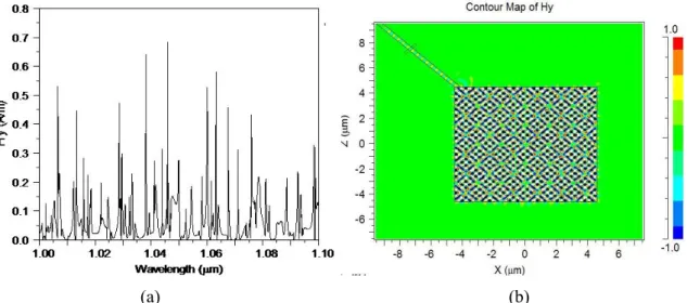
Considering a basic square resonator, the magnetic field spectrum in the waveguide is shown in Fig.
2(a). There are many resonant peaks in the free-space wavelength ( ) range between 1000 nm and
1100 nm. However, the high quality factor (Q) peaks appear at 1006.7 nm (Q=14000, mode TE1,72),
1017.3 nm (Q=20000, mode TE6,72), 1022 nm (Q=20000, mode TE5,70), 1038.1 nm (Q=20000, mode
TE0,72), 1043.9 nm (Q=16000, mode TE10,68 ), 1045. 9 nm (Q=20000, mode TE3,69), 1064.2 nm
(Q=20000, mode TE2,70), 1067.5 nm (Q=15000, TE0,70), 1098 nm (Q=20000, mode TE1,66). Figure 2(b),
3(a) and 3(b) show the Hy (y-component of the magnetic field distribution) at = 1006.7 nm, 1038.1
nm and 1043.9 nm, respectively. Based on these plots, we can clearly see that the waves have main
component of the magnetic field (Hy) with a null along the diagonals. Besides that, we can see that the
mode patterns form domains in the square resonator, i.e., they are packed in small regions with
square resonator. At 1006.7 nm, we can observe six domains along the x-direction, while at 1038.1
nm, we can observe five of these domains. These domains are more complex at 1043.9 nm but we can
still identify six domains along the x-direction. A displacement of the power source in the simulation
shifts these resonant wavelengths only slightly (less than 0.5 nm).
(a) (b)
Fig. 2. Basic square resonator of 9.1 µm: (a) Magnetic field spectrum (Hy) at the center of the
waveguide. (b) Magnetic field (Hy) distribution at λ = 1006.7 nm.
(a) (b)
Fig. 3. Basic square resonator of 9.1 µm : (a) Magnetic field (Hy) distribution at λ= 1038 nm. (b)
Magnetic field (Hy) distribution at λ = 1043.9 nm.
In order to assess vertical losses, we launched 3D FDTD simulations. The peaks at 1006.7 nm (mode TE1,72), 1038.1 nm (mode TE0,72), 1043.9 nm (mode TE10,68 ) appeared at1006.2 nm (Q=12000),
1037.4 nm (Q=18000) and 1041.4 nm (Q=14000), respectively. Power budget analyses indicate that
the power coupled into the waveguide for the modes TE1,72 , TE0,72 and TE10,68 are 36%, 42% and 57%,
respectively. The vertical losses account (in average) for about 3% of the input power escaping
through the air layer and 6% escaping through the oxide layer; the remaining percentage of the input
power is radiated laterally. The main reason for not launching only 3D FDTD simulations is that they pushed our computer resources to the limit, both in terms of memory and computation time (3D
few selected cases.
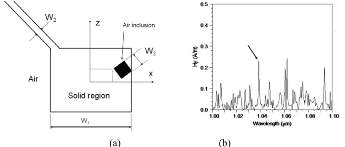
III. MODIFIED SQUARE RESONATOR WITH THE ADDITION OF AN AIR REGION
The occurrence of these domains is interesting and to further analyze these domains we envisaged
the following scheme: we replaced one of these domains by a rhombic air region (actually a square air
region rotated by 45 degrees). This is shown in Fig. 4(a), where the rhombic air region is placed close
to the rightmost side of the square. Because of the symmetry of the square resonator, it doesn’t make
much difference if we place these rhombic air regions adjacent to any of the sides of the square
resonator, the main difference is that the coupling efficiency into the waveguide may vary a little bit.
This rhombic region emulates, approximately, a magnetic wall region[24]. The position of the
rhombic inclusion (air region) with respect to a given side, on the other hand, changes the spectral
resonances of the square resonator. We aimed to analyze the effects of the rhombic inclusion in two
modes: TE0,72 (mode A) that has “well” ordered domains and TE10,68(mode B) with not so “ordered”
domains.
Let us consider initially the effects of the addition of the air region in a node position of mode A,
replacing it by an air inclusion. We optimized both the position and size (dimension W3) of the air
rhombic inclusion (the word position refers to the position of the leftmost edge of the inclusion, as
shown in Fig. 4(a) It should be mentioned that the optimum values of the size and position of the air
rhombic inclusion are highly dependent upon the mode. The optimum values depend on the given
mode, because the number of domains depends not only upon the dimensions of the square resonator
but also on the mode characteristics (a gross way to understand this is to remember that the number of
nodes and peaks in a certain resonator depends upon the electromagnetic resonant mode). In case of
modes A and B, the optimum size of the inclusion is about 1.1 m, implying that the size of each
domain is about 1.1 m.
(a) (b)
Fig. 4. Square resonator with an air rhombic section (rotated square region) replacing the domain of
mode A (a) schematic, (b) Magnetic field spectrum (Hy) at the center of the waveguide. The rhombic
air inclusion is located at x= 3.45 µm and z=-2.6 µm.
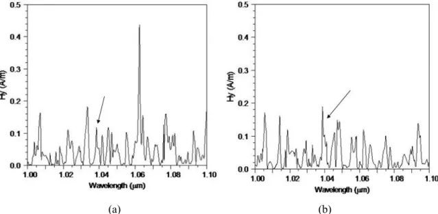
the air inclusion touches the rightmost side of the square resonator). The z coordinates in Figs. 4(b), 5(a) and 5(b) are z=-2.6 m, z=-0.9 m and z= 2.78 m, respectively. These positions were optimized to produce the maximum quality factor for mode A and make the air inclusion to overlap a domain of mode A (there are five similar domains along the x-direction. Beginning from the leftmost side of the square resonator, we can observe two half domains and 4 full domains for mode A, but the two “central” domains have similar spectral response. For this reason, we present only three spectral
responses in the waveguide). In all these Figs., the quality factor of mode A is about 3000. The main reason for the reduction of the quality factor of this mode is that the introduction of the air inclusion
leads to additional radiation losses. The field intensity in the waveguide is stronger when z= -2.6 m but not much different from the case when z= 2.78 m. There is no strong mode selectivity by introducing this air inclusion, since we can clearly see many other modes with similar quality factors.
Based upon these results, it seems that the actual size of the domain for mode A is indeed about 1.1 m.
Much more interesting results arise when we place an air inclusion at the domains of mode B. The domains for mode B (TE10,68 ) are not as well ordered as in the case of mode A, as can be observed in
Fig. 3(b). Although we obtained similar spectra by either placing the air inclusion closer to the edges
of the square resonator or close to the side center, the best result was obtained when we placed the air
inclusion close to the center of the rightmost side of the square. The Hyfield spectrum is shown in Fig. 6(a), where the air inclusion is located at (x=3.45 m, z= -0.12 m), close to the center of the square. There are several peaks, in the region between 1000 nm and 1100 nm, with quality factors of about
1000. These peaks can be observed, for example, at 1005.3 nm, 1029.9 nm and 1032.2 nm. However,
there is a main peak at 1044 nm (which shifts to 1043.4 nm in 3D simulations) with a quality factor of
6600 (2D simulations) and 5600 (3D simulations), which corresponds to the resonant wavelength of
mode TE10,68.In this case, the introduction of an air inclusion to mode B was much more selective (a
factor of difference of nearly 5:1 between the quality factors of different modes). Since this mode has
much higher Q than the remaining peaks, this laser device will be essentially single-mode over a wide
(a) (b)
Fig. 5. Square resonator with an air rhombic section (rotated square region) replacing the domain of
mode A: (a) Magnetic field spectrum (Hy) at the center of the waveguide. The rhombic air inclusion is
located at x= 3.45 µm and z=-0.9 µm. (b) Magnetic field spectrum (Hy) at the center of the waveguide.
The rhombic air inclusion is located at x= 3.45 µm and z=2.78 µm.
The magnetic field distribution (Hy) at 1044 nm is shown in Fig. 6(b). We can note that the addition of the air region distorts the magnetic field, but there is resemblance to the field distribution shown in
Fig. 3(b). Besides that, the air inclusion is definitely not a perfect magnetic wall: there is some
leakage into the air rhombic region. A 3D power budget analysis indicates that about 30% of the input power is coupled into the waveguide, with about 4% escaping through air and 8% through the oxide
region, the remaining power is lost laterally. This reduction of power coupling seems to indicate that
the radiation losses increased with the introduction of the air region.
(a) (b)
Fig. 6. Square resonator with an air rhombic section (rotated square region) replacing the domain of
mode B: (a) Magnetic field spectrum (Hy) at the center of the waveguide. The rhombic air inclusion is
located at x= 3.45µm and z=-0.12 µm. (b) Field distribution at λ=1044 nm.
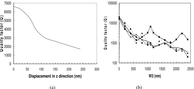
respect to the positions of minimum magnetic field what can lead to additional radiation losses. It is
evident that if we displace this air inclusion to another domain of the selected mode, we will return to
the situation where the edges of the inclusion match the positions of minimum magnetic field and the
quality factor will be high again. However, if we change slightly (hundreds of nanometers) the
z-position of the air inclusion, we won’t be in this situation and we clearly observe that the quality
factor drops with the z-displacement. Based upon Fig. 7(a), we may argue that a displacement from
the optimum position of 100 nm can be tolerated, leading to a reduction of Q to about 3500.
(a) (b)
Fig. 7. Square resonator with an air rhombic section (rotated square region) replacing the domain of
mode B: (a) Quality factor (Q) as a function of the displacement of the air inclusion, with respect to the
optimum point, along the z-direction. (b) Quality factor (Q) as a function of the size of the air inclusion
W3.
In Fig. 7(b), we change the size of the air inclusion (W3). The effect of the size of the air inclusion
on several modes is assessed. The effects on the resonant modes at 1022 nm, 1038.1 nm, 1043.9 nm
(selected mode), 1045.9 nm and 1063.2 nm are represented by the plots with dotted line with
triangular markers, solid line with no markers, solid line with squared markers, solid line with
x-markers and dotted line with circular x-markers, respectively. We can clearly note the oscillations in
these plots as will be explained later, but let us concentrate on the plot of solid line with squared
markers that represent the effect of the air inclusion on the selected mode. A very small air inclusion
has no major effects on the square resonator. As the size of the air inclusion increases, it critically
disturbs the points of high magnetic field what leads to increasing radiation losses and reduction of
the quality factor of this mode. However, as the size of the air inclusion increases, there will be a
point where the edges closely match the points of minimum magnetic field (this happens at
approximately W3= 1060 nm) and the perturbation to the magnetic field is not so high and leads to a high Q. The same happens when the air inclusion covers four domains (at W3=2200 nm), but at this stage, the introduction of such a large scatterer leads to significant higher radiation losses. This
explains the appearance of “oscillations” in the plot. Finally, it should be said that a variation of 100
0 1000 2000 3000 4000 5000 6000 7000
0 50 100 150 200 250 300
Displacement in z direction (nm)
Q
u
a
lit
y
fa
c
to
r
(Q
)
100 1000 10000 100000
0 500 1000 1500 2000 2500
W3 (nm)
Q
u
a
lit
y
f
act
o
r
(Q
nm in W3 can be tolerated by the square resonator. The addition of two air inclusions in the square
resonator leads to a lower Q because of larger radiation losses when two scatterers are introduced.
IV. STEADY-STATE ANALYSIS OF THE MODIFIED SQUARE RESONATOR WITH THE ADDITION OF AN AIR
REGION.
The steady-state response of the modified square resonator with an air inclusion to select mode
TE10,68 can be obtained by solving the rate equations (4.a) and (4.b) [7], [18], [25], [29], [30]. In the
active layer, we have three 7.4 nm thick In0.2Ga0.8As quantum wells. Since this epitaxially grown layer is primarily targeted for optically pumped sources, we will analyze the response of this laser device to
an external laser source (vertically reaching the device). The rate equations that describe the
performance of the device are given by [31],
AN BN CN
G N S V c h P dt dN a o p in ) ( 32
(4.a) pS
BN
S
N
G
dt
dS
2)
(
(4.b)where N is the carrier density, S the photon density, Pin is the pump power and the remaining
parameters are summarized in Table 1.
TABLE I.PARAMETERS AND ITS VALUES
Symbol Quantity Typical value
η Absorption ratio of
pump in QW region
0.26
p Pump wavelength 670 nm
h Planck’s constant . m kg/s
co Free-space speed of light
299792458 m/s
η Coupling efficiency 0.3
A Linear
recombination rate
. S
B Bimolecular
recombination coefficient
. m /s
C Auger nonradiative
recombination rate
m /s
Γ Confinement factor 0.22
β Spontaneous
emission factor
The pumped active volume (Va) depends on the parameters of the pump laser beam (spot-size
diameter) and the active region thickness. The thickness of the active region is different from the
thickness of the active/core layer [30], including mainly the quantum wells and confinement and
o l p
c Q
2
(5)
where
l is the emitting wavelength. The gain G(N) for quantum wells can be expressed as [32],( ) g oln
tr N
G N v G
N
(6)
where
v
g is the group velocity,G
o
1.5 10
x
5m
1is the gain coefficient andN
tr
1.5 10
x
24m
3 is the transparency carrier concentration.The final task is to solve the rate equations (3.a) and (3.b). A fourth-order Runge-Kutta method
could be employed to solve these equations, but further simplification can be obtained by assuming
that, under steady-state, dS/dt=dN/dt=0. Once we obtain the steady-state photon density S, the output power will be given by [25], [32],
mod
o e
out a
l mirror
hc
V
P
S
(7)where
a is the coupling efficiency to the ridge, Vmode is the optical mode volume and
mirror
pis the mirror lifetime.
Not all the output power is coupled into the single-mode waveguide. However, finite-difference
time-domain (FDTD) simulations can provide us information about the coupling efficiency into the
waveguide (
wg). The power coupled into the waveguide is then given by,wg wg out
P
P
(8)Note that
P
wgis the total power coupled into the waveguide.The threshold values of the laser devices can also be determined by using linear electromagnetic
analysis [33], i.e., the threshold is reached when the gain compensates the losses in the cavity. In this
sense, the threshold power of the laser devices can be determined given that gain is added to the
numerical FDTD method. The main characteristics of the mode are determined by applying Green’s
Fig. 8. Power guided into the waveguide.
We assume that the pump beam spot-size diameter is 10 m (typical value that can be reached by
our micro-photoluminescence setup). The power guided into the waveguide is shown in Fig. 8. Based
upon this analysis, the threshold pump optical power is about 3.9 mW and we might be able to couple
a few mW into the single-mode waveguide.
V. CONCLUSIONS
We have analyzed the modal domains in square resonators. These domains repeat themselves in the
large square and are very dependent upon the resonant mode.We estimated the size of the domains by
either observing the electromagnetic field distribution or adding an air inclusion to the square
resonator. The addition of the air inclusion can lead to quasi single-mode operation over a wide range
of wavelengths and over wide range of pumping power.
ACKNOWLEDGMENT
The author gratefully acknowledges the financial support to this project by the Australian Research
Council (ARC). Ziyuan Li acknowledges the UNSW internal fellowship.
REFERENCES
[1] O. Painter, R. K. Lee, A. Scherrer, A. Yariv, J. D. O’Brien, P. D. Dapkus, “Two-dimensional photonic bandgap defect mode laser, “ Science 284, 1819-1821, Jun. 1999.
[2] H. G. Park, J. K. Hwang, J. Huh, H. Y. Ryu, S. H. Kim, J. S. Kim, and Y. H. Lee, “ Characteristics of modified single-defect two-dimensional photonic crystal lasers, “ IEEE J. Quantum Electron. 38, 1353-1365, Oct. 2002.
[3] D. S. Song, S. H. Kim, H. G. Park, C. K. Kim, and Y. H. Lee, “ Single-fundamental-mode photonic crystal vertical-cavity surface-emitting lasers, “ Appl. Phys. Lett. 80, 3901-3903, May 2002.
[4] T. Asano, M. Mochizuki, S. Noda, M. Okano, and M. Imada, “ A channel drop filter using a single-defect in a 2D photonic crystal slab: defect engineering with respect to polarization mode and ratio of emission from upper and lower sides,” J. Lightwave Technol. 21, 1370-1376, May 2003.
0
0.2
0.4
0.6
0.8
1
1.2
1.4
1.6
0
2
4
6
8
10
12
14
Pin (mW)
Pw
g
(
mW
[5] S. Fan, S. G. Johnson, J. D. Joannopoulos, C. Manolatou, and H. A. Haus, “Waveguide branches in photonic crystals,” J. Opt. Soc. Am. B 18, 162-165, Feb. 2001.
[6] C. Seassal, C. Monat, J. Mouette, E. Touraille, B. Ben Bhakir, H. T. Hattori, J. L. Leclercq, X. Letartre, P. Rojo-Romeo, P. Viktorovitch, “InP bonded membrane photonics components and circuits: toward 2.5 dimensional micro-nano-photonics,” IEEE J. Sel. Top. In Quantum Electron. 11, 395-407, March /April2005.
[7] H. T. Hattori, H. H. Tan, and C. Jagadish, “Optically pumped in-plane photonic crystal micro-cavity laser arrays coupled to waveguides,” IEEE/OSA J. Lightwave Technol. 26, 1374-1380, Jun. 2008.
[8] R. M. Cazo, C. L. Barbosa, H. T. Hattori, and V. M. Schneider, “Steady-state analysis of a directional square lattice band-edge photonic crystal laser,” Microw. Opt. Technol. Lett. 46, 210-214, August 05 2005.
[9] H. T. Hattori, C. Seassal, X. Letartre, P. Rojo-Romeo, J. L. Leclercq, P. Viktorovitch, M. Zussy, L. di Cioccio, L. El Melahoui, and J. M. Fedeli, “Coupling analysis of heterogeneous integrated InP based photonic crystal triangular lattice band-edge lasers and silicon waveguides,” Opt. Express 13, 3310-3322, May 2005.
[10]C. Genet and T. W. Ebbesen, “Light in tiny holes,” Nature 445, 39-46, Jan. 2007.
[11]E. Laux, C. Genet, T. Skauli, and T. W. Ebbesen, “Plasmonic photon sorters for spectral and polarimetric imaging,” Nature Phot. 2, 161, Feb. 2008.
[12]N. Yu, E. Cubukcu, L. Diehl, M. A. Belkin, K. B. Crozier, F. Capasso, D. Bour, S. Corzine and G. Hofler, “Plasmonic quantum cascade laser antenna, “ Appl. Phys. Lett. 91, 173113, Oct. 2007.
[13]A. Minovich, H. T. Hattori, I. McKerracher, H. H. Tan, D. N. Neshev, C. Jagadish and Y. S. Kivhsar, “Enhanced transmission of light through periodic and chirped lattices of nanoholes, “ Opt. Comm. 282, 2023-2027, May 2009. [14]M. Fujita, A. Sakai, and T. Baba, “Ultra-small and ultra-low threshold GaInAsP–InP microdisk injection laser- design,
fabrication, lasing characteristics and spontaneous emission factor, “ IEEE J. Sel. Top. Quantum Electron. 5, 673-681, May/Jun.1999.
[15]A. F. J. Levi, R. E. Slusher, S. L. McCall, J. L. Glass, S. J. Pearton, and R. A. Logan, “Directional light coupling from microdisk lasers, “ Appl. Phys. Lett. 62, 562-563, Feb.1993.
[16]S. V. Boriskina, T. M. Benson, P. D. Sewell, and A. I. Nosich, “Directional emission, increased free spectral range, and mode Q-factors in 2-D wavelength-scale optical microcavity structures, “ IEEE J. Sel. Top. Quantum Electron. 12, 1175-1182, Nov. /Dec. 2006.
[17]H. T. Hattori, C. Seassal, E. Touraille, P. Rojo-Romeo, X. Letartre, G. Hollinger, P. Viktorovitch, L. DiCioccio, M. Zussy, L. El Melhaoui, and J. M. Fedeli, “Heterogeneous integration of microdisk lasers on silicon strip waveguides for optical interconnects, “ IEEE Phot. Technol. Lett. 18, 223-225, Jan. 2006.
[18]H. T. Hattori,”Analysis of optically pumped equilateral triangular microlasers with three mode-selective trenches,” Appl. Optics 47, 2178-2185, Apr. 2008.
[19]S. Ando, N. Kobayashi, and H. Ando, “Triangular-facet lasers coupled by a rectangular optical waveguide, “ Jpn. J. Appl. Phys. 36, L76-L78, Feb. 1997.
[20]Y. Z. Huang, W. H. Guo, and Q.M.Wang, “ Analysis and numerical simulation of eigenmode characteristics for semiconductor lasers with an equilateral triangle micro-resonator, “ IEEE J. Quantum Electron. 37, 100-107, Jan. 2001. [21]Y. Z. Huang, W. H. Guo, L. J. Yu, and H. B. Lei“ Analysis of semiconductor microlasers with an equilateral triangle
resonator by rate equations, “ IEEE J. Quantum Electron. 37, 1259-1264, Oct. 2001.
[22]W. H. Guo, Y. Z. Huang, Q. Y. Lu, L. J. Yu, “ Mode quality factor based on far-field emission for square resonators, “ IEEE Phot. Technol. Lett. 16, 479-481, Feb. 2004.
[23]H. T. Hattori, D. Liu, H. H. Tan, and C. Jagadish, “ Large square resonator laser with quasi-single-mode operation, “ IEEE Phot. Technol. Lett. 21, 359-361, Mar. 2009.
[24]W. H. Guo, Y. Z. Huang, Q. Y. Lu, and L. J. Yu, “Whispering-gallery-like modes in square resonators,” IEEE J. Quantum Electron. 29, 1106-1110, Sep. 2003.
[25]H. T. Hattori, “Modal analysis of one-dimensional nonuniform arrays of square resonators,” J. Opt. Soc. Am. B 25, 1873-1881, Nov. 2008.
[26]W. H. Guo, Y. Z. Huang, Q. Y. Liu and L. J. Yu, “Modes in square resonators,” IEEE J. Quantum Electron. 39, 1563-1566, Dec. 2003.
[27]D. Ohnishi, T. Okano, M. Imada, and S. Noda, “Room temperature continuous wave operation of a surface-emitting two-dimensional photonic crystal diode laser, ” Opt. Express 12, 1562-1568, Apr. 2004.
[28]W. Chang, A. Ankiewics, J. M. Soto-Crespo and N. Akhmediev, “Dissipative soliton resonances,” Phys. Rev. A 78, 023830, 2008
[29]N. Djellali, I. Gozhyk, D. Owens, S. Lozenko, M. lebental, J. Lautru, C. Ulysse, B. Kippelen, and J. Zyss, “Controlling the directional emission of holey organic microlasers,” Appl. Phys. Lett. 95, 101108, 2009.
[30]Fullwave 4.0 RSOFT design group, 1999, http://www.rsoftdesign.com