A HIGH THROUGHPUT AMBA AHB
PROTOCOL
1
MS. USHA A. JADHAV
Lecturer (Dept. of E&TC) D. Y. Patil COE, Akurdi, Pune-44
2
PROF. M. M. JADHAV
Asst. Professor (Dept. of E&TC) Sinhgad COE, Vadgaon Bk.
Off Sinhgad Road, Pune-41
Abstract
FPGA technology has been widely used for many application areas such as high throughput on-chip IO interfacing. One key factor for success in such vast diverse application space is the flexibility to configure the on-chip fabric and make it highly integrated. This paper presents an illustrative case of AMBA AHB bus that can be modeled as interface to various memories like SDR SDRAM and DDR SDRAM to work as master and LCD as a slave is simulated and synthesized for performance. This work results in the development of SoC integrated AMBA AHB bus that shows significant improvement in performance in terms of Data rate/throughput. The result concludes that in DDR SDRAM system Data rate is doubled as compared to SDR SDRAM system during write operation and during read operation the Data rate is six times than that of SDR SDRAM system for CAS latency of two, without increasing the clock rate or increasing the bus width to the memory cell.
Keywords: FPGA, AMBA AHB, SDR SDRAM, DDR SDRAM, LCD, ASB
I. Introduction
At the heart of an ever-increasing number of embedded applications is a ARM CPU. This is the first ARM processor developed specifically for FPGAs. It is intended for use in set-top boxes, Internet appliances and game consoles, smart mobile phones, palm-top computers, modems and other handheld applications that require high performance. This is provided through AMBA AHB bus which acts as the high performance system backbone bus for System on Chip (SoC) applications. Developments in manufacturing techniques and innovations in deep sub-micron technology have made possible applications with large on-chip memories. Designs are targeted at increasingly higher frequencies as well. The number of masters and slaves on the AHB bus are also increasing and are becoming increasingly more complex. While designing with the AHB bus, design, verification and synthesis must take care of certain issues, which, if not handled carefully, lead to higher NRE costs and re-spins. The AMBA AHB implements features required for high- performance and high clock frequency systems including:
Burst transfers Split transactions
Single cycle bus master handover Single clock edge operation Non-tristate implementation Pipelined bus
Wider data bus configurations (64/128 bits).
II. Background of SoC Communication Architectures
Several protocols currently enjoy a certain degree of popularity. AMBA (Advanced Microcontroller Bus Architecture) [1], is a bus standard devised by ARM with aim to support efficient on-chip communications among ARM processor cores. IBM's CoreConnect [2] is supported by a vast set of tools that allow the automatic generation of many parts of the system. The performance and flexibility offered by the protocol are interesting, but it remains one of the most complex embedded bus architectures, leading to design effort overhead. The "open" Wishbone [2] specification, released by Silicone, offers a set of guidelines for a basic, simple bus structure. This protocol has been selected by the OpenCores Web site as the standard to follow for the development of the free IP library that they are building.
III. Related Works about Developed IP Cores
As related work to ours, we cite the approach in [3] shows that significant improvement in effective bandwidth and reduction in communication latency when compared with traditional single access buses. This is achieved in SAMBA-bus architecture for multiple compatible bus transactions that can be performed simultaneously with only a single bus access grant from the bus arbiter.
Since the SDR SDRAM Controller [4] and DDR SDRAM Controller [5] is a module that will be used with other design pieces in the FPGA, the utilization and timing numbers reported in this section are just estimates. As they are combined with other pieces of the FPGA design, the utilization of FPGA resources and timing of the SDR SDRAM Controller and DDR SDRAM Controller design will vary from the result.
Many tasks can be done by either a customized FSMD or a microcontroller. The tradeoff is between the hardware complexity, performance and ease of development. There is no exact rule on which one to choose. Because developing software is usually easier than creating customized hardware, the PicoBlaze microcontroller option is generally preferable for non-time-critical applications. Thus, the use of FSMD and PicoBlaze microcontroller will reduce the hardware complexity, increases performance and provides ease of development. The principle purpose of this document [6] is to illustrate how PicoBlaze can be used to control the LCD display and given an exercise which states that “Implement a hardware state machine which can perform the LCD initialization sequence. Compare the size of your implementation with the 96 slices required to implement a PicoBlaze processor.”
The LCD driver IP [7] with dot matrix scalable capability can interface to AMBA on chip bus is implemented by hardware description language as a RTL design. The future scope given in this paper involves integrating more application software codes associated with the design of IP blocks forplatform based SOC verification.
Thus, we decided to design an AMBA AHB bus that can be modeled as interface to two different memories as master with output device like LCD as a slave.
IV. Structure require to Implement AMBA AHB
Fig.1 shows the structure required to implement an AMBA AHB design with two masters and two slaves.
The AMBA AHB bus protocol is designed to be used with a central multiplexer interconnection scheme. Using this scheme all bus masters drive out the address and control signals indicating the transfer they wish to perform and the arbiter determines which master has its address and control signals routed to all of the slaves. A central decoder is also required to control the read data and response signal multiplexer, which selects the appropriate signals from the slave that is involved in the transfer. The main components of this bus interconnection as shown in above Fig.1 are Arbiter, decoder, Master and Slave.
Arbiter:
The AMBA bus specification is a multi-master bus standard. As a result, a bus arbiter is needed to ensure that only one bus master has access to the bus at any particular point in time. Each bus master can request the bus; the Arbiter decides which has the highest priority and issues a grant signal accordingly. Thus, Arbiter works like as a traffic light controller for ambulance.
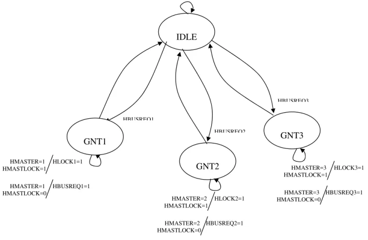
Fig. 2 shows the FSM diagram for AHB Arbiter. Each bus master can request the bus; the Arbiter decides which has the highest priority and issues a grant signal accordingly.
IDLE: Master gives request signal to the arbiter and a grant signal is issued to a highest priority master.
GNT1: This state indicates that the master1 is currently the highest priority master requesting the bus, taking into account locked transfers and SPLIT transfers.
GNT2: This state indicates that the master2 is currently the highest priority master requesting the bus, taking into account locked transfers and SPLIT transfers.
GNT3: This state indicates that the master3 is currently the highest priority master requesting the bus, taking into account locked transfers and SPLIT transfers.Fig. 2 FSM diagram for AHB Arbiter
IDLE
GNT3
GNT2
HBUSREQ1
HBUSREQ2
HBUSREQ3
HMASTER=1 HLOCK1=1 HMASTLOCK=1
GNT1
HMASTER=2 HLOCK2=1 HMASTLOCK=1
HMASTER=3 HLOCK3=1 HMASTLOCK=1
HMASTER=1 HBUSREQ1=1 HMASTLOCK=0
HMASTER=2 HBUSREQ2=1 HMASTLOCK=0
Decoder:
AHB decoderis used to decode the address of each transfer and provide a select signal for the slave that is involved in the transfer. A single centralized decoder is required in all AHB implementations. A decoder is implemented using one hot technique.
Master:
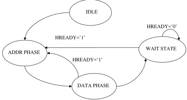
AHB masteris able to initiate read and write operations by providing an address and control information. Only one bus master is allowed to actively use the bus at any one time.(max. 16). Fig. 3 shows the FSM diagram for AHB Master. Following are the various states are to be carried out by the AHB master for their proper operation.
IDLE: Master gives request signal to the arbiter and indicates the current transfer type is IDLE.
ADDR PHASE: This state is used to provide address and control information.
DATA PHASE: According to control information i.e. HWRITE=1 master will broadcast data on the write data bus, HWDATA[31:0].
WAIT STATE: In this state, if hready is high which indicates that the current bus transaction is over and then go to address phase else be in same wait state.Fig. 3 FSM diagram for AHB Master
Slave:
AHB slaveresponds to a read or write operation within a given address-space range. The bus slave signals back to the active master the success, failure or waiting of the data transfer.
The FSM diagram for AHB Slave is shown in Fig. 4 where slave uses a HSELxselect signal from the decoder to determine when it should respond to a bus transfer. Following are the various states are to be carried out by the AHB slave for their proper operation.
IDLE: In this state, when Hsel=1 then next state will be address phase and gives an OKAY response, which indicates the successful completion of previous data transaction.
ADDR PHASE: This state is used to provide address and response information, taking into account locked transfer and split transfer.
DATA PHASE: According to response information slave will generate the data on the read data bus, HRDATA[31:0].IDLE
WAIT STATE
DATA PHASE
ADDR PHASE
HREADY=’0’
Fig. 4 FSM diagram for AHB Slave
V. System Implementation
In this section, we proposed a AMBA-AHB architecture which consists of two masters and one slave as shown in Fig.5.
Fig. 5 Block diagram of the system
IDLE
Hsel=’1’
Hselect
=’1
Hsel=’1’
Hsel=’1’
Hsel=’0’
Hsel=’0’
Hsel=’0’
For high performance i.e. more speed is required between ARM CPU and Flash memory because ARM7 runs at 80MHz and flash memory has access time 50ns. This leads to limits the execution speed by 20MHz. Thus the simplest is to load critical sections of your program into RAM. RAM has much faster access time. Thus, in our architecture we have chosen SDR SDRAM controller and DDR SDRAM controller as a Masters of AMBA AHB bus. The principle purpose of the selection of LCD controller as a slave is using PicoBlaze processor as the PicoBlaze processor is a compact 8-bit microcontroller core for Xilinx FPGA devices.
Features of SDR SDRAM Controller
PC100 compliant
Performs auto-refresh cycles
Supports single-beat and burst transactions
Supports various SDRAM data widths (8, 16, and 32 bits)
Interfaces to 256*32 on-chip SDRAM
Features of DDR SDRAM Controller
Programmable burst length of 2, 4 and 8
Programmable CAS latency of 2, 2.5 and 3
Burst length applies to both read and write
Uses CLK instead of DQS to receive data from the DDR
LCD Controller using Picoblaze Processor:
The PicoBlaze processor is a compact 8-bit microcontroller core for Xilinx FPGA devices. It is provided as a cell-level HDL description (which is known as soft core) and can be synthesized along with other logic. PicoBlaze is optimized for efficiency and occupies only about 200 logic cells, which amount to less than 5% resource of a 3S200 device. While not intended as a high-performance processor, it is compact and flexible and can be used for simple data processing and control, particularly for non-time-critical “house-keeping’’ and I/O operations.
The controller receives its display signal from a SDR SDRAM or DDR SDRAM and translates it into commands that are understood by the LCD module. This LCD is a 16 x 2 dot matrix liquid crystal display.
VI. Results and Discussions
The AMBA AHB Protocol can be modeled as interface to SDR SDRAM memory or DDR SDRAM memory as a master and LCD as a slave is discussed and implemented in Xilinx FPGA. The advantages of implementing this AMBA AHB in VHDL and FPGA as a target technology is that it gives the flexibility, upgradability and customization benefits of programmable logic devices.
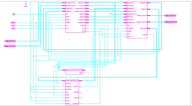
Fig. 6 RTL Schematic for AMBA AHB Bus
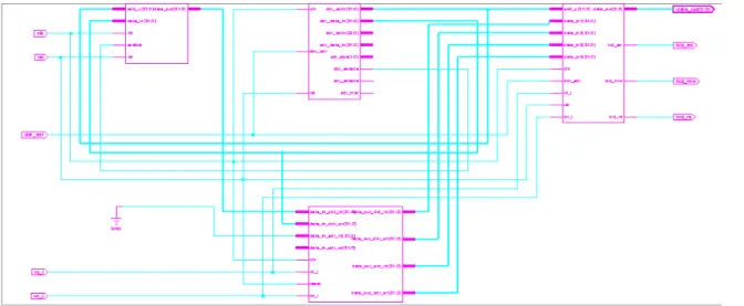
Fig. 7 shows the RTL Schematic for the SDR SDRAM system showing OS, SDR SDRAM top module, AMBA AHB and LCD Controller.
Fig. 7 RTL schematic for the SDR SDRAM system
Fig. 8 RTL schematic for the DDR SDRAM system
Optimization has been done in SDR SDRAM controller, DDR SDRAM controller and LCD controller for No. of Slices, No. of flip-flops and No. of LUTs as compared to OPB and summarized in the Table 1, Table 2 and Table 3 respectively.
Table 1: Percentage optimized utilization of SDR SDRAM Controller
OSB SDR SDRAM Controller OPB SDR SDRAM Controller
%Optimized Utilization Logic
Utilization
Used Available Utilization Min Max Max. % Utilization
No. of slices 65 4656 1% 198 416 8.93% 7.93%
No. of Flip Flops
91 9312 0% 200 510 5.47% 5.47%
No. of LUTs 70 9312 0% 309 482 5.17% 5.17%
Table 2: Percentage optimized utilization of DDR SDRAM Controller
OSB DDR SDRAM Controller OPB DDR SDRAM Controller [5]
%Optimized Utilization Logic
Utilization
Used Available Utilization Min Max Max. % Utilization
No. of slices 94 4656 2% 278 314 13.48% 11.48%
No. of Flip Flops
102 9312 1% 352 371 3.98% 2.98%
No. of LUTs 173 9312 1% 250 307 3.98% 2.98%
Table 3: Percentage optimized utilization of LCD Controller
LCD Controller LCD Display Control (
PicoBlaze)[6]
%Optimized Utilization Logic
Utilization
Used Available Utilization Used Available Utilization
No. of slices 64 4656 1% 113 4656 2% 1%
Table 4: Performance Comparisons
Sr. No. SDR SDRAM Top Module DDR SDRAM Top Module
1. No. of clock cycles for 32-bit data transactions
For Write operation= 05 For Read operation= 03
No. of clock cycles for 32-bit data transactions For Initialization=09
For Write operation= 05 For Read operation= 01
2. Data rate for Write operation= 8000MB/s
Data rate for Write operation= 16000MB/s
3. Data rate for Read operation= 13,333MB/s
Data rate for Read operation=80,000MB/s
VII. Conclusions
The AMBA AHB Protocol is modeled as interface to SDR SDRAM and DDR SDRAM memories and LCD is discussed and implemented in Xilinx FPGA. Optimization has been identified in SDR SDRAM controller, DDR SDRAM controller and LCD controller for No. of Slices, No. of flip-flops and No. of LUTs as compared to OPB. This work results in the development of SoC integrated AMBA AHB bus that shows significant improvement in performance in terms of Data rate/throughput for DDR SDRAM as compared to SDR SDRAM. Future research in this area will involve integrating more application software codes associated with the design of IP blocks for platform based SOC verification. We also intend to verify more complex SoC bus designs like AXI, multilayer AHB etc. using the methodology proposed in this paper.
VIII. References
[1] AMBA Specification Rev 2.0. ARM Ltd., 1999.
[2] Milica Mitic, and Mile Stojcev, "An Overview of On-Chip Buses", FACTA Universitatis Series: Electronics and Energetics, vol.19, no.3, pp 405-428, Dec 2006.
[3] Ruibing Lu, Aiqun Cao, and Cheng-Kok Koh, Senior Member, IEEE,” SAMBA-Bus:A High Performance Bus Architecture for System-on-Chips” IEEE Transactions on Very Large Scale Integration (VLSI) Systems, VOL. 15, NO. 1, JANUARY 2007,69
[4] Xilinx “OPB Synchronous DRAM (SDRAM) Controller” DS426 July 21, 2005.
[5] Xilinx “OPB Double Data Rate (DDR) Synchronous DRAM (SDRAM) Controller” DS424(V1.9.1) September 19, 2003. [6] Xilinx “Pico blaze Initial Design for Spartan-3E Starter Kit (LCD Display Control)” Ken Chapman Xilinx Ltd.16th February 2006. [7] Yu-Jung Huang, Chih-Feng Liu, Shao-Pin Chang, Feng-Yuan Chuang, Chang-Chan Chen Department of Electronic Engineering, I-Sho
University, Kaohsiung, Taiwan 80424, ROC, “Design of LCD driver IP for SoC Applications” 2004 IEEE Asia-Pacific Conference on Advanced System Integrated Circuits(AP-ASIC2004)/Aug. 4-5, 2004
[8] FPGA PROTOTYPING BY VHDL EXAMPLES, Xilinx SpartanTM
-3 Version, Pong P. Chu, Cleveland State University, A John Wiley & Sons, Inc., Publication 2008.