c
Copernicus GmbH 2003
Advances in
Radio Science
A Comparison of current SDRAM types: SDR, DDR, and RDRAM
B. Klehn and M. Brox
Infineon Technologies AG, Munich, Germany
Abstract. The ever increasing demand for bandwidth of computer-systems lead to several standards of SDRAMs. This article compares SDR, DDRI, DDRII, and RDRAM systems. Besides the overall basic innovations, differences will be discussed. Topics like architecture, interfaces, and modules are described.
1 Introduction
Over the last years the clock rate of a microprocessor in a typ-ical desktop PC has exceeded the 2 GHz number. To feed the processor and the other active components in such a system with data, the memory sub-system has to be able to provide the data sufficiently fast. To achieve this goal, multiple in-novations had been introduced and integrated into ever more powerful devices. On the other hand, important basic con-cepts have remained in use over various generations. In this article, we intend to describe differences and commonalities of the various main-memory types and discuss reasons for the changes. In this respect, we will start with a discussion of the basic concept of a DRAM cell.
2 Basic DRAM functionality
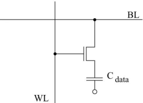
The memory cell of a DRAM consists of a capacitor and a se-lect transistor (Fig. 1). The binary information is stored as a charge on the capacitor. Cells are oriented along a matrix of parallel bitlines and perpendicular wordlines. The read-out of a memory cell is shown in Fig. 2. To prepare for the read-out, bitlines are pre-charged to an intermediate level, which generally is set at half of the array operation voltage. The read-out starts with decoding the externally supplied row-address into a physical wordline. Asserting this wordline opens the select transistor. As the voltage on the storage ca-pacitor is either lower (logical ‘0’) or higher (logical ‘1’) the Correspondence to: B. Klehn
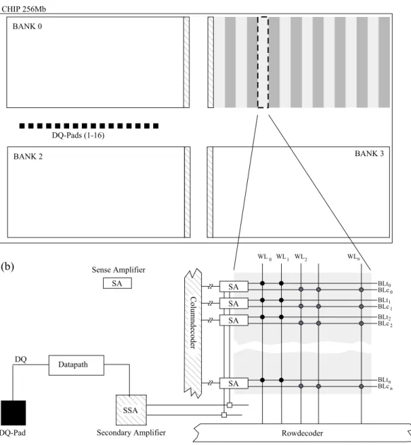
voltage on the BL changes during this process. As an ex-ample, Fig. 2 shows the read-out of a ‘1’ causing the bitline voltage to increase (trace BLt). Typical values for a stor-age capacitor are in between 20 fF and 40 fF, which is much lower than the value for the parasitic bitline capacitance (be-tween 100 fF and 200 fF). Therefore, the voltage change on the bitline is relatively small – often in the order of some 10 mV, only. To be able to securely read the cell, the voltage change is amplified in the differential sense-amplifier which compares voltage on the bitline BLt with the voltage on a neighbouring, floating bitline BLc. At the end of a sense-amplification, all cells of one wordline are read out and read-out information has been amplified to digital values. Selec-tion of the sense-amplifier to be read is performed through the column-decoder. Dependent on the column-address, one sense-amplifier gets connected to the data-lines over the ar-ray, re-amplified in a second amplifier stage and driven to-wards the output buffers (Fig. 3).
A common method to achieve a continuous data-stream from a DRAM is the so-called burst-mode. Here, multiple data are read-out from one line of sense-amplifiers one after another. The memory controller has to supply only the ad-dress of the first read access; the DRAM internally generates all the subsequent column-addresses. In its simplest imple-mentation, however, this continuous stream would have to stop the moment a new wordline would have to be activated. Activation of a different wordline requires bringing down the old wordline, precharging the bitlines and asserting the new wordline.
applica-266 B. Klehn and : A Comparison of current SDRAM types: SDR, DDR, and RDRAM
Fig. 1. Schematics of a memory cell build from a storage capacitor
and a select transistor. The select transistor connects the capacitor with the bitline BL. Activation of the select transistor is performed through wordline WL.
Fig. 2. Bitline voltage as a function of time during read-out of a
memory cell. Example shows read-out of a ‘1’ from a cell attached to BLt. At a, wordline gets asserted and charge from the memory cell flows onto the bitline. The neighbouring bitline BLc gets capac-itively coupled high. At b, charge transfer from the cell is complete and the sense-amplifier can get activated. After sense-amplification at around 40 ns, digital levels are present on BLt and BLc.
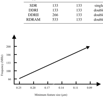
tions, peak bandwidth cannot be sustained. Often word-lines need to be activated in the same bank. In this case the de-lay encountered by the array pre-charge cannot be hidden. Activation of wordlines, sensing and pre-charging are domi-nated by parasitic delays as heavily loaded, yet narrow lines in the array need to be driven. Shrinking device dimensions yielded only a performance improvement of a factor around 3 (see Fig. 4). This is rooted in the fact that devices as imple-mented in DRAMs need to follow other device design guide lines such as e.g. devices in logic processes. As the number of DRAMs in a memory system is often very large, the stand-by current has to be as low as possible, which forces one to use transistors with some 100 mV of threshold voltage. To close the gap between the processor and the memory, circuit techniques have to be employed, which will be discussed in the following section.
3 Clock synchronization
Older memory devices up to 66 MHz used an external asyn-chronous interface. The memory itself did not have an ex-ternal clock input. Any activity was purely edge-triggered and commands could be issued at any arbitrary time as long as the internal time constants of the memory were met. For higher frequency operation, to help ensure reliable input of data, addresses, and commands, an external clock has been used. Typically, the memory samples the input lines at the rising edge of the clock. Commands can, thus, be issued to the memory at only multiples of the clock cycle time. Legal command combinations are described in detail in the data-sheet of the manufacturer. Use of an external clock marked the introduction of the so-called SDRAM.
3.1 SDR
Standardized SDRAMs input commands and addresses at the rising edge of the clock. In a first development step, input and output of data was also possible at the rising clock-edge, only (Fig. 5). This concept permits a single data transmission per clock cycle and consequently led to the name of Single-Data-Rate-SDRAM (SDR-SDRAM). The clocksignal itself is single-ended. Output of the data itself was not specifically synchronized to this clock. The only requirement is that fol-lowing the clock edge for a minimum time oftOH the previ-ous data is held valid, while aftertAC new data is available. To give typical values for a 133 MHz-SDR-SDRAM,tOH = 3 ns, andtAC= 5.4 ns. In between, no valid data is present on the bus.
3.2 DDR
The natural evolution of this concept towards higher band-width, is to allow input and output of data at twice the rate. This scheme as shown in Fig. 5 is called Double-Data-Rate (DDR). DDRI and DDRII-SDRAMs derive their name from this data transmission approach.
Fig. 3. (a) Sketch of the architecture of a typical 256 Mb-DRAM. Memory cells are laid out in four memory banks of 64 Mb. Each bank
can be treated as a partially independent memory. (b) Sub-division of one 64 Mb-bank into 4 Mb-units. The row-decoder selects one WL. Through column-decoding, one sense-amplifier gets selected to drive data towards the data-path.
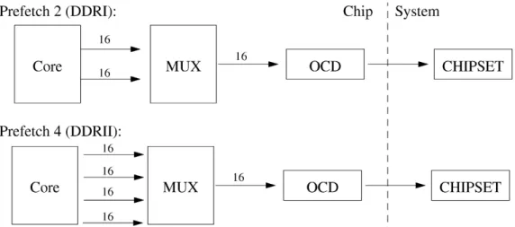
4 Prefetch
A memory using the DDR output-scheme has to deliver up to 16bit for each half clock cycle. This could be imple-mented by reading out the array twice per clock-cycle. At a clock rate of 200 MHz this would be equivalent to a read-out rate of 400 MHz which could be facilitated if the array is partitioned into very small sub-units with short bitlines and short wordlines. Short bitlines, however, require a high num-ber of sense-amplifiers and short wordlines a high numnum-ber of row-decoders on the chip. A more typical solution is to prefetch 2×16 bit in one array-access for one DDR clock-cycle (more precise: 2×-prefetch). Under this condition, core frequency can be held constant at 200 MHz, while
data-rate achieves 400 Mb/s per pin. Figure 6 illustdata-rates the prin-ciple, which also leads to a simple extension path towards even higher bandwidths while still keeping core frequency constant. RDRAM in contrast, uses an 8×-prefetch to reach a data-rate of 1066 Mb/s per pin while running the core at a relaxed 133 MHz-frequency. Time-multiplexing circuitry in the chip has to guarantee only that prefetched data is driven out in the correct order.
5 Differences in the concepts
268 B. Klehn and : A Comparison of current SDRAM types: SDR, DDR, and RDRAM
Table 1. Performance summary of the relevant architectures. Typical values for frequency is given
Typ Clock(MHz) Core(MHz) Scheme Datarate per pin (Mb/s) Prefetch Data-width
SDR 133 133 single 133 none 64
DDRI 133 133 double 266 2 64
DDRII 266 133 double 533 4 64
RDRAM 533 133 double 1066 8 16
Fig. 4. Operation frequency improvement through smaller feature
size. Improvement is around a factor of 3 going from 0.25µm to 0.09µm.
Fig. 5. The graph depicts the external clock inputs for SDR and
DDRI/DDRII. The crossing of CLK and bCLK defines the point of time t1 much more fail-safe compared to the edge of a single ended clock.
to sustainable values for each architecture, the frequency of the data lines is differing strongly. Here, architectural differ-ences between the different types are becoming relevant. The following section will touch upon these.
5.1 Commands and requests
The memory controller needs a way to initiate activity in the memory. The classical way is the simple command protocol
as implemented on the evolutionary SDR/DDR family of de-vices. All control and address information for one command in the DRAM is transmitted during a single clock cycle. This protocol requires typically 5 control- and 15 address-lines to encode all relevant commands (e.g. activate row, precharge row, read column, write column, ...). In this approach, the complexity of the address and control lines is limited because these lines are run in single-data-rate fashion, however, on the expense of a rather large number of lines. Another ad-vantage is the small latency: complete decoding of the com-mand can procede after only one clock cycle. RDRAMs fol-low a completely different approach. Here, e.g., a single set of eight lines for addresses and control may be used. Three of these lines transmit row oriented requests; five transmit column oriented requests. The three row-oriented lines han-dle row activation and row precharge. To be able to encode an e.g. 16bit wide address onto 3 lines, the information is time-multiplexed and transmitted in DDR-like fashion. On a first look this introduces multiple disadvantages. Four clock cycles are required to transmit all information required in one access, which increases access latency compared to the one-clock cycle approach of SDR/DDR devices. Furthermore, a capture-DLL needs to be implemented as the data-eye onto the shared control, data, and address lines (the bus) gets too narrow to be received with conventional means. As, however, the number of lines gets very small, the bus can be run at very high frequency while still keeping total system cost at a reasonable level. In addition, seperation of the bus into row-request and a column-row-request sections enables a very flexible protocol: row and column operations can be initiated inde-pendent from and parallel to each other. For example, it is possible to issue a read to bank 0 and an activate to bank 1 in parallel.
5.2 Module design
Fig. 6. Prefetch: Capturing of 2x resp. 4x the required data volume and time-multiplexing it onto the output leads to a simple multiplication
of the external data-rate of the memory device.
RDRAM:
16 bit 16 bit 16 bit 16 bit 16 bit
Module 64 bit
16 bit 16 bit 16 bit 16 bit
Module SDR/DDRI/DDRII:
Controller
Controller
Fig. 7. SDR- and DDR-modules are operating in desktop-systems with a data-width of 64 bit and address typically 8 devices in parallel. The
RDRAM-bus is significantly narrower (16 bit) and only one device is addressed. RDRAM bandwidth is increased by running the bus at a very high clock-frequency.
higher-frequency RDRAM bus gets obvious. On the other hand, RDRAMs are forced to operate at higher clock-rate because for a given clock-rate a DDR-system would be able to deliver four times the RDRAM peak bandwidth simply because of the 64 bit data-width.
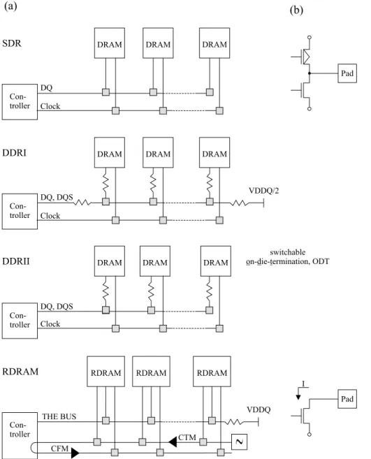
5.3 Termination, clocking and strobing
As discussed before, SDR-systems are using a simple, single-ended external clock signal. All data lines are non-terminated and no specific additional means exist to improve signal quality and data valid window. Output drivers are simple voltage source push-pull type drivers. On chip-level, DDR and RDRAM implement DLLs for better alignment of the data output. However, differences do not stop here but continue on the architectural level. Figure 8 shows the clock-ing and output schemes realized in the different advanced DRAM types.
DDRI uses a mid-level termination of all lines.
Addition-ally, stub-resistors are introduced to limit reflections. A fur-ther, important change is the introduction of the data-strobe signal (DQS). DQS is a bi-directional synchronization sig-nal, which is generated by the controller during a write ac-cess to the memory and by the memory during a read-acac-cess to the controller. In this way, DQS travels in the same di-rection as the data signal, itself. DQS is generated in a way that each edge (rising and falling) indicates valid data. As the flight time is the same for DQS and DQ, both controller and memory can use the DQS signal to capture incoming data. Different arrival times of the uni-directional always-on clock signal can thus be effectively cancelled out.
270 B. Klehn and : A Comparison of current SDRAM types: SDR, DDR, and RDRAM
Fig. 8. Data line topologies for the different DRAM types (a): SDR, DDRI, DDRII, and RDRAM. (b) Simplified final driver stage.
RDRAMs employ a very different scheme. A clock is gen-erated at the far end of the bus. The CTM-clock travels in the direction of the controller, gets mirrored-back at the con-troller and afterwards travels as CFM-clock on its way back to the far end of the bus. These two clocks can be used to synchronize write data to the memory with CTM, and read-data from the memory with CFM. In this scheme, travel di-rection of relevant clock and data is the same such that flight time differences are cancelled out. A high level termination is present only at the far-end of the bus such that the con-troller represents an open end to the bus. At this open end signal reflection occurs, which has to be accounted for in the RDRAM system design. Especially, RDRAM drivers need to be designed with a high differential output resistance such that no second reflection occurs when a reflected wave passes a data-driving memory. This can be guaranteed by designing
the output-driver as a current source, which makes its design very much different than the SDR/DDR voltage mode driver. Signaling levels are currents of 0 mA for a logical ’0’ and typically 30 mA for a logical ‘1’. Only on the data lines, the travelling current wave translates to a travelling voltage wave which can be received by memory respective controller.
6 Chip area
DDRI and quadrupled for DDRII. The package-oriented communication between a controller and an RDRAM re-quires a complex decoder logic block in the I/O part. The reduced supply voltages of emerging products adds to the area because of complicated on-chip pump and generator systems.
7 Outlook
It is possible to run the core of an SDRAM with frequencies of 133, 166 or even more than 200 MHz. Combining it with a high prefetch and a large number of parallel devices, data rates in the region of several gigabytes per second are possi-ble. Otherwise to have a noticeable speed up in a computer
system all components of such a system have to be balanced. With these bandwidth image processing and simulations are possible at high level. To enter new sophisticated applica-tions a higher operating speed of computer systems is still desirable.
Acknowledgements. The Authors thanks H. Ruckerbauer, R. Klein, and E. Brass for the detailed discussions.
References
Itoh, K.: VLSI Memory Chip Design, Springer-Verlag, Berlin Hei-delberg New York, 2001.