742 Brazilian Journal of Physics, vol. 29, no. 4, December, 1999
Metal-Insulator Transition at B=0 in an AlGaAs/GaAs
Two-Dimensional Electron Gas under the Inuence
of InAs Self-Assembled Quantum Dots
E. Rib eiro 1;2
, R. Jaggi 2
, T.Heinzel 2
, K. Ensslin 2
,G. Medeiros-Rib eiro 3
, and P. M. Petro 3
1 Instituto de Fsica \Gleb Wataghin", UNICAMP, 13083-970 Campinas, SP, Brazil 2 Solid State Physics Laboratory, ETH Zurich, CH-8093 Zurich, Switzerland 3 Materials Department, University of California, Santa Barbara, CA 93106, USA
Received 27 May, 1999
We report the observation of a metal-insulator transition in zero magnetic eld in a two dimensional electron gas under the inuence of a plane of InAs self-assembled quantum dots located at 30 A below the AlGaAs/GaAs heterointerface. The transition is observed as a function of temperature and electric eld at B=0. A scaling analysis yields exponents similar to those obtained for Si MOSFET's . We suggest that the disorder introduced by the quantum dots plays a crucial role.
I Introduction
In an important paper of 1979 based on scaling the-ory of localization, Abrahamset al. have shown that
a two-dimensional system without interactions was ex-pected to behave as an insulator in zero-magnetic eld [1]. Since then, it has been a general belief that there is no metallic regime in 2D at T = 0, contrary to what happens in the 3D case. The metal-insulator transi-tion (MIT) at B = 0, rst reported for a Si metal-oxide-semiconductor eld-eect transistor (MOSFET) by Kravchenko et al. [2], has thus generated a great
interest in the eld. Experimentally, the MIT was fur-ther conrmed not only in Si MOSFET's [3-6] but also for holes in SiGe quantum wells [7] and holes in Al-GaAs/GaAs structures [8,9]. All the samples used there were optimized towards low disorder (clean samples) and large electron-electron (e-e) interaction (large ef-fective carrier masses). It was also clear that a scaling analysis of the data (as a function of temperature or electric eld) is essential to characterize the metallic and the insulator states [4], even when including inter-actions [10,11].
Coulomb interaction is believed to be in the heart of the MIT [12,13] and, in fact, the reported ratio Ee,e=EF is of the order of 10 for a MIT [3-9]. Very
recently, however, we have reported on the observation of a MIT in an AlGaAs/GaAs two-dimensional electron gas (2DEG) under the inuence of InAs self-assembled
quantum dots (SAQD) [14]. This result is striking be-cause our samples' parameters are rather dierent from the ones in the previous studies. First, the 2DEG is highly disordered due to the proximity of the SAQD. Second,
Ee,e
EF /
m
"p
Ns
(1) and, for electrons in GaAs, one has a smaller eective mass mand a slightly higher dielectric constant " than
in the previous papers. Since the present MIT occurs for about the same carrier density Ns, in our samples
the e-e interaction energy Ee,e is of the order of the
electronic kinetic energy EF (Ee,e=EF
'0:9). It seems
unlikely that this weak e-e interaction could be solely responsible for the observed metallic phase. In this pa-per we show the results of a scaling analysis and suggest that the presence of the SAQD mightdrive the observed MIT.
The samples used in this work are described in de-tail in Ref. 15. A layer of InAs SAQD is embedded 30 A from the interface AlGaAs/GaAs where the 2DEG forms. Since the substrate was not rotated during the growth of the dot layer, we found a gradient of dot den-sity across the wafer [15]. We will concentrate on the rst and second highest dot density samples, A (110
11
dots/cm2) and B (7:9 10
10 dots/cm2). Gated
E. Rib eiroetal. 743
of a dilution refrigerator (base temperature 60 mK). Standard low-frequency lock-in techniques were used to measure the four-point resistivity, keeping the current as low as 1 nA. A dc setup was also used for double-checking and no quantitative dierences were found.
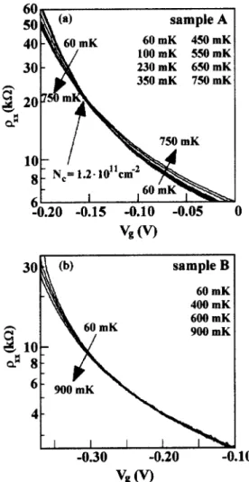
Figure 1. Temperature dependence of the resistivity as a function of gate voltage for samples (a) A and (b) B. A crossing point of the traces in (a) characterizes a MIT.
Fig. 1 shows traces of the longitudinal resistivity
xxas function of gate voltage, taken at increasing
tem-peratures T for samples A [Fig.1(a)] and B [Fig. 1(b)]. The last exhibits the \usual" behavior for 2DEG's: the resistivity increases as the temperature decreases (the insulator behavior predicted by Abrahams et al. [1]),
for all the measured N
s. Sample A however, shows a
crossing point of the resistivity traces at a critical car-rier density N
c = 1 :210
11 cm,2. This crossing point
occurs close to xx =
h=e
2 and divides the data into
two distinct regions: N s
<N
c, where
xx decreases for
increasing T (insulator); and N s
>N
c, where
xx
sur-prisingly increases for increasing T, characterizing the
existence of a metallic phase. Although being similar to the data of Kravchenkoet al. [3], the temperature
dependence of
xx is weak in our sample. As a
conse-quence, the crossing point is blurred and an error bar should be included forN
c.
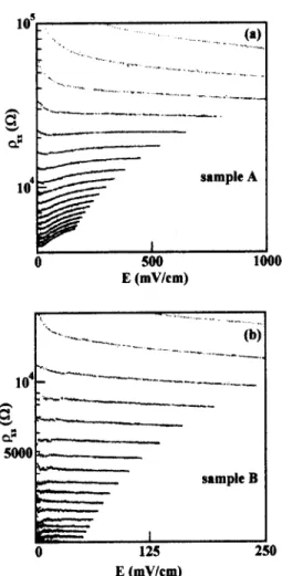
A similar feature is observed for the electric-eld (E) dependence of
xxfor a xed T. Fig. 2 shows
XX
vs. E traces for dierent N
s plotted from the original ivs. V curves. Again, sample A [Fig. 2(a)] exhibits a
region where
xx decreases for decreasing E (metallic),
in addition to the usual insulator behavior is present. Sample B, in other hand, shows no signs of a metal-lic phase, consistent with the T-dependence data. The
xx vs. N
s traces for increasing current (not shown)
exhibit a crossing point similar to the one in Fig. 1(a), atN
c= 1 :2910
11cm,2.
To further reinforce that our data shows an actual MIT we carried out a scaling analysis. According to Ref. 4, the resistivity is expected to scale with temper-ature as
xx( T;N
s) = f jj=T 1 z (2) and with electric eld as
xx( E;N
s) = g jj=E 1 (z +1) ; (3)
where = (N s
,N
c) =N
c,
(z) is the correlation
length (dynamical) exponent [16]. Comparing the re-sults of both scaling processes it is possible to determine the exponents separately. Let us focus on the data of Fig. 2(a). Scaling according to (3) would be success-ful when by choosing the appropriate exponent 1
(z +1)
all the curves collapse into two distinct (metallic and insulator) branches. Fig. 3 shows
xx as a function of j j
T 1
(z +1)
corresponding to the best collapse of the data of Fig. 2(a), which yields(z+1) = (4:50:3).
Apply-ing the same procedures to the T dependence of xx,
we nd z = (2:60:8) (the large error bar reects
the uncertainty inN
c, as discussed above). The nal
values for the scaling exponents arez= (1:41:2) and = (1:91:1), in the same range as those reported
for Si MOSFET's [4]. They also approach the theoret-ical valuesz= 1 (interacting system [16]) and= 4=3
744 Brazilian Journal of Physics, vol. 29, no. 4, December, 1999
Figure 2. Nsdependence ofxxas a function of the electric
eld for samples (a) A and (b) B.N
s values, from top to
bottom: (a) 0.75 to 3.2210
11cm,2; (b) 0.87 to 3.11 10
11
cm,2.
There are also dierences with respect to the previ-ous MIT. First, the metallic phase is not destroyed by a parallel magnetic eld up to 12 T. Second, samples from the same wafer but with lower dot density didn't displayed any MIT, making it clear that a high SAQD density is needed for this phenomenon. At present we don't have a full understanding of the metallic phase in sample B14. Its high density of SAQD means a high number of negatively charged scattering centers (up to 2 electrons per dot [15]), which goes against the main assumption of a recent model for Si MOSFET proposed by Altshuler and Maslov [17]. In this paper the authors propose that charge traps in the oxide layer could be neutralized as N
s increases, leading to less scattering
and thus driving the MIT. In our case the situation is opposite. Since the wafer is homogeneous except for the SAQD layer and no MIT was found for low dot density samples, the dominant scattering mechanism are the SAQD, which are populated before the 2DEG starts to
form. Thus the higher the SAQD density the higher is the scattering [15] and the suggestion of Ref. 17 is dif-cult to apply. The quantum dots lled with electrons could enhance spin interactions, recently suggested to be essential to the formation of a metallic phase [12]. We have also proposed an explanation in terms of qua-sibound minibands that might form in the continuum of the quantum dots and within the range of the Fermi energy [14]. These states could scatter resonantly the electrons of the gas [18], thus increasing the resistivity. Decreasing the temperature would decrease the number of available states for scattering and thus the resistiv-ity would decrease, giving rise to the observed metallic phase.
Figure 3. Resistivity of sample A as a function of the scal-ing argument to show the collapse of the traces into metallic and insulator branches.
In summary, our experimental data clearly show the occurrence of a MIT at B = 0 in a 2DEG under the in-uence of InAs SAQD. A scaling analysis yields results that are in agreement with previously reported values. We suggest that the special type of disorder in our sam-ples (the SAQD) might be responsible for the observed metallic phase. In this sense, the MIT in 2D systems remains a topic far from being understood, requiring more experimental as well as theoretical work.
References
[1] E. Abrahams, P. W. Anderson, D. C. Licciardello, and T. V. Ramakrishnan, Phys. Rev. Lett.42, 673 (1979).
[2] S. V. Kravchenko, G. V. Kravchenko, J. E. Furneaux, V. M. Pudalov, and M. D'Iorio, Phys. Rev. B50, 8039
(1994).
[3] S. V. Kravchenko, W. E. Mason, G. E. Bowker, J. E. Furneaux, V. M. Pudalov, and M. D'Iorio, Phys. Rev. B51, 7038 (1995).
[4] S. V. Kravchenko, D. Simonian, M. P. Sarachik, W. Mason, and J. E. Furneaux, Phys. Rev. Lett.77, 4938
(1996).
[5] D. Simonian, S. V. Kravchenko, M. P. Sarachik, and V. M. Pudalov, Phys. Rev. Lett.79, 2304 (1997).
[6] D. Popovic, A. B. Fowler, and S. Washburn, Phys. Rev. Lett.79, 1543 (1997).
[7] J. Lam, M. D'Iorio, D. Brown, and H. Lafontaine, Phys. Rev. B56, R12741 (1997).
[8] M. Y. Simmons, A. R. Hamilton, M. Pepper, E. H. Lindeld, P. D. Rose, D. A. Ritchie, A. K. Savchenko, and T. G. Griths, Phys. Rev. Lett.80, 1292 (1998).
[9] Y. Hanein, U. Meirav, D. Sahar, C. C. Li, D. C. Tsui, and H. Shtrikman, Phys. Rev. Lett.80, 1288 (1998).
[10] A. M. Finkel'stein, Zh. Eksp. Teor. Fiz.84, 163 (1983)
[Sov. Phys. JETP57, 97 (1983)].
[11] V. Dobrosavljevic, E. Abrahams, E. Miranda, and S. Chakravarty, Phys. Rev. Lett.79, 455 (1997).
[12] V. M. Pudalov, JETP Lett.66, 175 (1997).
[13] S. He and X. C. Xie, Phys. Rev. Lett.80, 3324 (1998).
[14] E. Ribeiro, R. Jaggi, T. Heinzel, K. Ensslin, G. Medeiros-Ribeiro, and P. M. Petro, Phys. Rev. Lett.
82, 996 (1999).
[15] E. Ribeiro, E. Muller, T. Heinzel, H. Auderset, K. En-sslin, G. Medeiros-Ribeiro, and P. M. Petro, Phys. Rev. B58, 1506 (1998).
[16] S. L. Sondhi, S. M. Girvin, J. P. Carini, and D. Shahar, Rev. Mod. Phys69, 315 (1997).
[17] B. L. Altshuler and D. L. Maslov, cond-mat/9807245. [18] T. V. Shahbazyan and S. E. Ulloa, Phys Rev. Lett.79,