Brazilian Journal of Physics, vol. 36, no. 2A, June, 2006 369
Conductance of Three-Dimensional Cross Junctions in the
Quantum Ballistic Regime
Luis C. O. Dacal1 and Erasmo A. de Andrada e Silva 2
1Instituto de Estudos Avanc¸ados - IEAv - CTA, C. P. 6044, 12228-001, S ˜ao Jos´e dos Campos - SP, Brazil and 2Instituto Nacional de Pesquisas Espaciais - INPE, C. P. 515, 12201-970, S ˜ao Jos´e dos Campos - SP, Brazil
Received on 4 April, 2005
The influence of dimensionality on the conductance of semiconductor cross junctions is investigated in the effective mass approximation and quantum ballistic regime. Our calculations exhibit some similar features for both two- and three-dimensional models, namely the conductance peaks before the fundamental eigenenergy of the quantum wire that represents the sidearms and the zero conductance dip. Despite this, we show that, in general, the conductance and the electronic wave function are strongly affected when the third spatial dimension is taken into account. In other words, we prove that two-dimensional models are not suitable for representing this kind of system.
Keywords: Influence of dimensionality; Conductance; Effective mass approximation
I. INTRODUCTION
The experimental observation of conductance quantization in semiconductor point contacts [1, 2] was one of the most im-portant manifestations of quantum mechanics in mesoscopic systems. The measurement of integer numbers of a quantum of conductance (G0=2e2/h) is a consequence of the cur-rent equipartition in a small number of propagating modes [3]. Very early, this phenomenon was satisfactorily repro-duced through two-dimensional (2D) models [4, 5].
More recently, significant attention has been devoted to electronic conductance in quantum cross junctions [6] and four terminal systems [7]. What is more, this geometry has been exploited in proposals for spintronic devices [8, 9], in which, spin is the essential property for device operation [10]. Despite the fact that spin-orbit interaction implies spin and spatial coordinates mixing [11], the theoretical works keep on employing 2D models [8, 9].
In this work, we show that, even in absence of spin effects, the conductance of cross junctions obtained through three-dimensional (3D) models is qualitatively distinct from that given by 2D ones.
II. MODEL
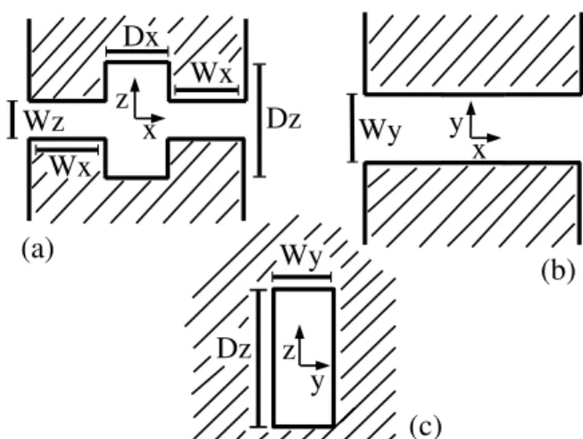
We consider a cross junction limited by infinite potential barriers. Figure 1 shows the cross-sections of the 3D system at y=0 (a), z=0 (b) and x=0 (c) planes. The axes origin is the center of the cross and the 3D model has specular symmetry with respect to the xz, xy and yz planes. Figure 1-(a) repre-sents the 2D system.
The effective mass and envelope function approximations are used throughout this paper. We consider ballistic transport regime and a GaAs structure, what meansm∗=0.067 for the channel and contacts.
Let us assume the electron incident from the left (x<0), with energy E0. The use of infinite barriers uncouples the electron dynamics in the three directions. As a consequence,
a combination of quantum well and free particle eigenstates is used to build the wave function in each junction region, namely contacts, sidearms and central region. For exam-ple, the electronic wave function in the source reservoir (x<
−Wx−Dx/2 ) is given by:
ΨL(~r) =
eikxx+ikzzφl(y) +
+
∑
n
φn(y)Z +∞
−∞ dk ′ z
n
An(k′z)e−ik
′
xx+ik′zzo, (1)
where~k= (kx,kz)is the initial wave vector andφi(y)is theith quantum well eigenstate in the source contact (see section III). An(kz′)are the coefficients of the reflected partial waves due to the electron scattering at the channel entrance. Notice that energy conservation imposes sum overall transverse states, which means evanescent modes are also included.
Fig. 1. Schematic representation of the cross junction system. Three cross-sections are shown: at y=0 plane (a), at z=0 plane (b) and at x=0 plane (c). Figure (a) also represents the 2D model.
370 Luis C. O. Dacal and Erasmo A. de Andrada e Silva
of continuity of the wave function and the flux at each inter-face, one obtains a system of equations that determines the wave function coefficients, like theAn(k′z)in equation 1 [12]. Considering zero temperature and a weak potential difference between the contacts, the conductance can then be calculated through equation 12 of reference [5]. The mathematical de-tails will be published elsewhere.
III. RESULTS AND DISCUSSION
The dimensions of the 3D system analyzed here areWx= 500 ˚A,Wy=200 ˚A,Wz=1000 ˚A,Dx=1000 ˚A andDz=1800 ˚A (see figure 1). The convergence of the calculated conduc-tance was obtained using, in the channel region, a basis set with 8 and 3 quantum well states for the z and y directions, respectively. In order to obtain these results, we used a wide quantum well (>>Wy) to discretize the contacts continuum in y direction. This allowed us to access the 2D to 3D crossover through the increase of this quantum well width. When it is equal toWy, we verified that the 2D results are re-obtained just shifted in energy through the fundamentalWy quantum well eigenvalue. It proves that this energy is the suitable one for shifting the 2D results when comparing them with the 3D ones. As a first result, we reproduced previous 2D calculations for the above parameters [5].
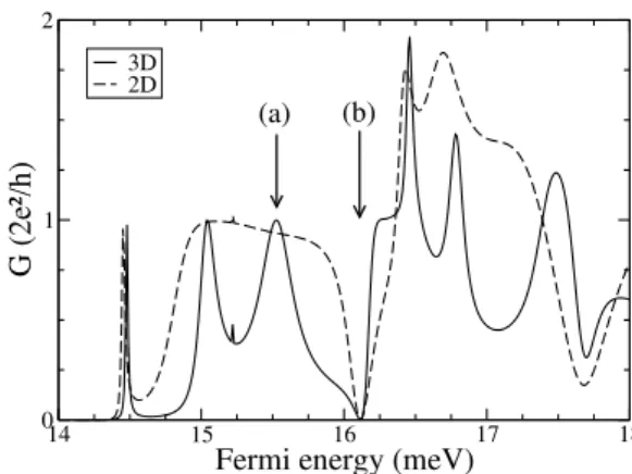
In Figure 2 we show the calculated conductance for the above mentioned 2D and 3D systems as a function of the elec-tronic Fermi energy. It is important to say that our calculations exhibit a smooth transition from 2D to 3D results (not shown), proving that the obtainedqualitativedifferences are not model artifacts.
At the same time, some features are present in both 2D and 3D calculations, namely the zero conductance at 16.11 meV and the first narrow peaks. These peaks appear, in figure 2, at 14.48 meV (3D) and 14.455 meV (2D), that is below the fundamental eigenenergy of the quantum wire that represents the sidearms, but above the corresponding one for the central region of the cross junction [5]. This is an explicit indication of evanescent modes contribution to the cross junction prop-erties. On the other hand, the zero conductance occurs at the same energy for both systems. This kind of interference effect was previously observed [5, 13, 14].
Despite these similarities, figure 2 shows that, in general, the conductance of 2D and 3D cross junctions are qualita-tivelydifferent. This is a consequence of the extreme sensitiv-ity of these systems to their geometric characteristics. Small changes in their shape and dimensions will induce a tremen-dous effect on the conductance and wave function [15]. As an example, in figure 3, we show the|Ψ(x)|2in the central region of the cross junction for the 2D (dashed line) and 3D (full line) systems considered in figure 2, where the chosen energy is highlighted by the arrow (a), namely 15.53 meV. As one can see, the square of the wave function for the 3D sys-tem indicates a much more localized state if compared to the 2D case. Considering that the 2D and the 3D systems exhibit
equivalent densities of probability when the contact width in y is equal toWy(not shown), one can conclude that the main cause for the different behaviors of 2D and 3D cross junc-tions is the electron scattering at the entrance and exit of the channel, introduced in the 3D model when the contact width becomes much bigger thanWy.
14 15 16 17 18
Fermi energy (meV) 0
1 2
G (2e²/h)
3D 2D
(a) (b)
Fig. 2. Conductance of a cross junction as a function of Fermi en-ergy. Results for 2D (dash line) and 3D (full line) systems are shown. The junction dimensions are :Wx=500 ˚A,Wy=200 ˚A,Wz=1000
˚A,Dx=1000 ˚A,Dz=1800 ˚A. The arrows (a) and (b) indicate the
energy values used in figures 3 and 4 respectively. The fundamen-tal eigenenergy of theWy=200 ˚A quantum well was added to the
energy scale of the 2D results.
-400 -200 0 200 400
Position in x (Å) 40
60 80 100
Normalized
|ψ(
x
)|
² (x100)
3D 2D
Fig. 3. The normalized probability density in the central region of the cross junction as a function of x for the 2D (dashed line) and 3D (full line) systems considered in the previous figure. The chosen energy is 15.53 meV, as indicated by arrow (a) in figure 2.
Brazilian Journal of Physics, vol. 36, no. 2A, June, 2006 371
for 2D and 3D cross junctions, namely a strongly localized state in the central region of the system.
-400 -200 0 200 400
Position in x (Å) 0
20 40 60 80 100
Normalized
|ψ(
x
)|
² (x100)
3D 2D
Fig. 4. The as same figure 3, but for 16.11 meV as indicated by arrow (b) in figure 2.
Despite these similarities, we can say that, in general, cross junctions can not be properly described through 2D models.
Consequently, the current use of 2D simulations for spintronic devices [8, 9] must be reviewed.
IV. CONCLUSIONS
We employed the effective mass approximation to calculate the conductance of semiconductor cross junctions in the quan-tum ballistic regime. We obtainedqualitativelydistinct results for the conductance and wave function when 2D and 3D mod-els are considered. Moreover, we argue that the main reason for these differences is the electron scattering at the entrance and exit of the channel. To sum up, our results prove that 2D models are not suitable for cross junction description.
Acknowledgments
This work was supported by FAPESP (Brazil) and CNPq (Brazil).
[1] B. J. van Wees, H. van Houten, C. W. J. Beenakker, J. G. Williamson, L. P. Kouwenhoven, D. van der Marel, and C. T. Foxon, Phys. Rev. Lett.60, 848 (1988).
[2] D. A. Wharam, T. J. Thornton, R. Newbury, M. Pepper, H. Ahmed, J. E. F. Frost, D. G. Hasko, D. C. Peacock, D. A. Ritchie, and G. A. C. Jones, J. Phys. C21, L209 (1988).
[3] C. W. J. Beenakker and H. van Houten, Solid State Physics44,
1 (1991).
[4] George Kirczenow, Phys. Rev. B39, 10452 (1989).
[5] Karl-Fredrik Berggren and Zhen-li Ji, Phys. Rev. B43, 4760
(1991).
[6] C. H. Yang, M. J. Yang, K. A. Cheng, and J. C. Culbertson, Phys. Rev. B66, 115306 (2002).
[7] C.-T. Liang, O. A. Tkachenko, V. A. Tkachenko, D. G. Bak-sheyev, M. Y. Simmoms, D. A. Ritchie, and M. Pepper, Phys. Rev. B70, 195324 (2004).
[8] E. N. Bulgakov, K. N. Pichugin, A. F. Sadreev, P. Stˇreda, and P.
ˇ
Seba, Phys. Rev. Lett.83, 376 (1999).
[9] L. Sheng, D. N. Sheng, and C. S. Ting, Phys. Rev. Lett.94,
016602 (2005).
[10] I. ˇZuti´c, J. Fabian, and S. Das Sarma, Rev. of Modern Phys.76,
323 (2004).
[11] E. A. de Andrada e Silva and G. C. La Rocca, Phys. Rev. B67,
165318 (2003).
[12] J. A. Brum, Phys. Rev. B43, 12082 (1991).
[13] A. R. Rocha and J. A. Brum, Braz. Jour. Phys.32 (2A), 296
(2002).
[14] D. G. Ravenhall, H. W. Wyld, and R. L. Schult, Phys. Rev. Lett.
62, 1780 (1989).
[15] K.-F. Berggren, C. Besev, and Zhen-Li Ji, Physica ScriptaT42,