L.M. Camarinha-Matos et al. (Eds.): DoCEIS 2014, IFIP AICT 423, pp. 585–591, 2014. © IFIP International Federation for Information Processing 2014
Constant G
mOperational Amplifier, at 0.4 V Operation,
Using the Low-Voltage DTMOS Technique
Joana Correia2, Nuno Mancelos2, and João Goes1,2
1
Centre for Technologies and Systems (CTS) – UNINOVA
2
Dept. of Electrical Engineering (DEE), Universidade Nova de Lisboa (UNL) Campus FCT/UNL, 2829-516, Caparica, Portugal
{jm.correia,n.mancelos}@campus.fct.unl.pt, [email protected]
Abstract. The use of the dynamic threshold MOS (DTMOS) technique is evaluated in a two-stage rail-to-rail Input/Output, constant ܩ amplifier. The proper choice of specific transistors in which the technique should be used is presented, as well as the resulting improvements, mainly regarding stability of the circuit at low voltage operation. The DTMOS technique is used in the NMOS transistors of the folded-cascode input stage, allowing the circuit to be stable at VDD = 0.4 V, with equivalent gain and gain-and-bandwidth product (GBW) values achieved with the same ܸ value, for the initial circuit operating at 0.8 V. The implemented changes allow the circuit to be stable at low voltage operations without requiring any increase in the cascoded-Miller compensation capacitors, saving circuit area and, consequently, cost.
Keywords: Low-voltage DTMOS technique, Low supply voltage OPAMP, Low-voltage OPAMP stability issues.
1
Introduction
The general tendency for reducing the supply voltage in ICs represents a challenge for analog amplifier designers, in terms of maintaining required gain levels, bandwidth (BW) and stability. In terms of stability and frequency compensation, several techniques can be implemented, but the solutions represent an increase of the circuit area, since they often include the need of additional capacitors.
The main objective of this work is to improve the gain, GBW and stability of the original amplifier, and to guarantee that the OTA still works, with reasonable performance, when operating at much lower supply voltages.
The DTMOS technique was the technique chosen to reach the objectives, and consists in connecting the bulk of a transistor to its gate terminal. This allows the bulk voltage to be variable, instead of being fixed at ground or VDD (NMOS or PMOS,
respectively) [2]. The transistor suffers from body-effect, in this configuration, since the voltage between the source and bulk terminals is not zero. However, the transcondutance that is a result of the body-effect contributes, positively, to the total transcondutance of the transistor, being this contribution an increase of approximately 20-to-30% of the transcondutance of the transistor. This means that in the DTMOS configuration, the body-effect of a transistor is not a degrading factor in its ܩ, but rather an improvement.
The disadvantages of using the DTMOS technique are the increase of the parasitic capacitances in the transistor, which can ultimately lead to a loss of circuit BW, and the possibility of a latch-up problem. In the case of this particular application and circuit, the latch-up situation is not a real problem, because there won’t be sufficient voltage to trigger the effect, since the intended test supply voltages will be lower than 0.7 V, which is the typical problematic threshold that allows that effect to be a problem. In terms of the increase of the parasitic capacitances, and consequent decrease in BW, the situation can be dealt with separately, although the changes in the parasitic capacitances are not relevant enough to reflect some problematic difference in terms of the BW.
2
Relationship to Collective Awareness Systems
Collective Awareness Systems that are capable of harnessing collective intelligence, allowing the creation of a network of distributed knowledge and data from real environments, include a multitude of individual subsystems that must be able to collect and transmit the actual information that is shared in the system. These subsystems may include a wide range of different devices and applications, but they usually consist in wireless and portable devices [3] for which concerns like power consumption and autonomous lifetime are very pertinent.
3
Amplifier Description
3.1 Initial Amplifier
The 0.8 V, rail-to-rail Input/Output, constant ܩ OTA, whose schematic is presented in Fig. 1, consists of two stages.
Fig. 1. Initial operational amplifier
The rail-to-rail folded-cascode input stage includes two differential pairs in parallel, consisting of the transistors M1, M2 (NMOS differential pair), M3 and M4 (PMOS). This configuration allows rail-to-rail operation at the input. For high common-mode voltages at the input, the NMOS differential pair is on, while for low common-mode voltages it is the PMOS differential pair that is on. For medium levels of the common-mode voltages, both differential pairs are on, increasing the current flowing to the summing circuit and consequently increasing the ܩ. To avoid this increase in the transcondutance, since it is desirable to have it constant for the whole range of common-mode voltages, the current switches M5 to M8 are added. The following folded-cascode configuration is responsible for the summing of the signals (current) coming from the complementary differential pairs.
The class AB output stage features, as stated above, the cascaded-Miller frequency compensation technique, which includes the capacitors CM1 and CM2. Class AB operations are made possible by M19 and M20. These transistors are driven by the signal currents coming from transistors M14 and M16 and are polarized by the diode-connected transistors M22, M23, M25 and M26. The output transistors M27 and M28 are in common-source configuration to allow rail-to-rail operations at the output. The M27 transistor functions at the positive swing, while M28 takes care of the negative swing. The frequency of non-dominant pole is shifted to higher frequencies by the cascoded-Miller frequency compensation technique.
3.2 Proposed Modifications in the Original Amplifier
of the PMOS and NMOS devices, respectively from ܸ and VSS, and re-connect them to the gate terminal [4, 5].
Many possible configurations have been simulated and evaluated, using the DTMOS technique applied to different sets of transistors. The best results, taking into account simplicity and gain results, were achieved using the DTMOS technique only in the NMOS cascode devices M13 and M14. Notice that the DTMOS technique also has the benefit of reducing the threshold voltage of the transistor. Since NMOS transistors have a higher threshold voltage than PMOS, it is understandable that it is preferable to use the DTMOS technique in the NMOS cascode transistors rather than in the PMOS. This requires fabrication processes either with triple-well or with deep-Nwell but this is clearly the case, for all state-of-the-art deep nano-scale CMOS technologies.
4
Amplifier Performance
4.1 Electrical Simulations of the Original Amplifier Circuit
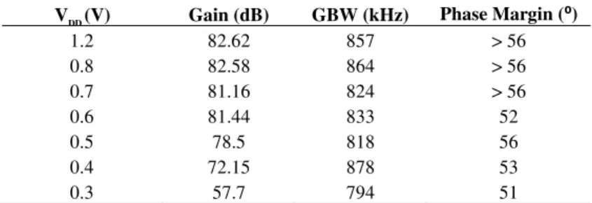
The simulation results achieved with the initial configuration of the circuit ported into the 130 nm CMOS technology (the original circuit, without the use of the DTMOS technique) are presented in Table 1. The presented results include simulations run under different supply voltages, focusing on the values of DC gain, GBW and Phase Margin (PM).
Table 1. Simulated results for the initial configuration of the amplifier circuit
VDD(V) Gain (dB) GBW (kHz) Phase Margin (⁰)
1.2 82.62 857 > 56
0.8 82.58 864 > 56
0.7 81.16 824 > 56
0.6 81.44 833 52
0.5 78.5 818 56
0.4 72.15 878 53
0.3 57.7 794 51
4.2 Re-Design of the Amplifier Using DTMOS
For the circuit amplifier including the proposed changes, the same simulations have been carried-out, under the same conditions (common-mode voltages at 55 % of ܸ, the PM measured with a closed-loop gain of 6 dB). The results are summarized in Table 2.
Table 2. Results for the new circuit configuration (DTMOS)
VDD (V) Gain (dB) GBW (kHz) Phase Margin (⁰)
1.2 80.37 887 > 60 (higher)
0.8 79.54 844 > 60 (higher)
0.7 79.14 902 (higher) > 60 (higher) 0.6 79.5 872 (higher) 57 (higher) 0.5 77.14 909 (higher) 61 (higher) 0.4 72.45 (higher) 924 (higher) 60 (higher) 0.3 58.82 (higher) 794 (same) 59 (higher)
As it can be observed in Table 2, there are just minor improvements in the DC gain and in the GBW. The most significant improvement is the PM parameter, particularly at very low supply voltages below 0.6 V. Since the values are superior to 55o, the OTA circuit is now stable for those ܸ values and can operate down to 0.3 V.
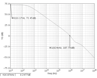
Fig. 2. Gain trace
by itself, a significant reduction in the supply voltage) and because it presents good gain, GBW and PM results, in comparison to the results achieved by the original circuit, for that same ܸ.
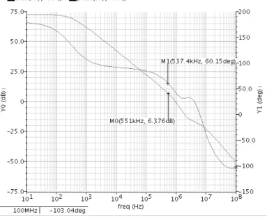
Fig. 3. Gain and Phase traces
5
Conclusions
It has been demonstrated in this paper that, using DTMOS in a couple of specific devices of a two-stage rail-to-rain Input/Output, constant Gm OTA can improve its
stability whilst operating at very low supply voltages. The proper choice of specific transistors in which the technique should be used has been presented, as well as the resulting improvements. The implemented changes allow the circuit to be stable at low voltage operations without requiring any increase in the cascoded-Miller compensation capacitors, saving circuit area and, consequently, cost.
The significant supply voltage reductions that can be achieved with this DTMOS technique are, therefore, quite promising for the hardware implementations of Collective Awareness Systems, in which amplifiers are of paramount importance, and where power consumption and cost (silicon area) are limiting factors.
References
1. Citakovic, J., Riis Nielsen, I., Hammel Nielsen, J., Asbeck, P., Andreani, P.: A 0.8V, 7μA, Rail-to-Rail Input/Output, Constant Gm Operational Amplifier in Standard Digital 0.18μm
2. Chatterjee, S., Pun, K.P., Stanić, N., Tsividis, Y., Kinget, P.: Analog Circuit Design Techniques at 0.5V. Springer (2007)
3. Bicocchi, N., Fontana, D., Mamei, M., Zambonelli, F.: Collective Awareness and Action in Urban Superorganisms, Italy (2013)
4. Abdollahvand, S., Gomes, A., Rodrigues, D., Januário, F., Goes, J.: Design of Robust CMOS Amplifiers Combining Advanced Low-Voltage and Feedback Techniques. In: Camarinha-Matos, L.M., Shahamatnia, E., Nunes, G. (eds.) DoCEIS 2012. IFIP AICT, vol. 372, pp. 421–428. Springer, Heidelberg (2012)