Carlos Manuel Ferreira Carvalho
MestreCMOS indoor light energy harvesting
system for wireless sensing
applications
Dissertação para obtenção do Grau de Doutor em Engenharia Electrotécnica e de Computadores
Orientador: Prof. Doutor Nuno Filipe Silva Veríssimo Paulino, Professor auxiliar, FCT/UNL
Júri:
Presidente: Prof. Doutor Luís Manuel Camarinha-Matos
Arguentes: Prof. Doutor Jorge Manuel dos Santos Ribeiro Fernandes Prof. Doutor João Carlos da Palma Goes
Vogais: Prof. Doutor Marcelino Bicho dos Santos
Prof. Doutor Nuno Filipe Silva Veríssimo Paulino Prof. Doutor João Pedro Abreu de Oliveira Prof. Doutor Vítor Manuel da Silva Costa
CMOS indoor light energy harvesting system for wireless sensing applications
Copyright © Carlos Manuel Ferreira Carvalho, Faculdade de Ciências e Tecnologia, Universidade Nova de Lisboa.
A Faculdade de Ciências e Tecnologia e a Universidade Nova de Lisboa têm o direito, perpétuo e sem limites geográficos, de arquivar e publicar esta dissertação através de exemplares impressos reproduzidos em papel ou de forma digital, ou por qualquer outro meio conhecido ou que venha a ser inventado, e de a divulgar através de repositórios científicos e de admitir a sua cópia e distribuição com objetivos educacionais ou de investigação, não comerciais, desde que seja dado crédito ao autor e editor.
A
CKNOWLEDGMENTS
After such a long journey, there are many who have contributed to the accomplishment of this thesis. I hope I do not omit anyone. If so, please forgive me, because certainly it is not on purpose. All of those who are mentioned here are important, according to their respective context so, when more than one name appears listed, the order of the list is not relevant.
First of all, I would like to enormously thank to my supervisor, Dr. Nuno Paulino. If it wasn’t because of him, the work that I developed during the last five years would not have happened. In that case, it would be very likely for me to think that the theme of Energy Harvesting was a subject for others to take care of, and not me. More than a supervisor, he has been someone who shed a lot of light over my knowledge about Electronics. I would like to thank him for all his help and patience, especially when helping me sorting out problems, when sometimes things appeared to be stuck at a dead end. More than a supervisor, he has also been a friend.
I would also like to thank to the members of my Thesis Accompanying Committee, Dr. João Goes, Dr. Jorge Fernandes and Dr. Nuno Paulino, for taking all their time and attention in the analysis of the working plan of my thesis, and for suggesting the necessary improvements to make it a better work, with an increased scientific added value.
Also, I’d like to express an increased acknowledgment to Dr. João Goes, for having accepted me into his research group, for providing me the necessary computational and laboratorial conditions to perform my work at UNINOVA and for having shared so much interesting and valuable knowledge during his classes and in our conversations.
Another person to whom I wish to thank is Dr. Guilherme Lavareda, for his cooperation regarding the subject of photovoltaic cells and for sharing so much valuable information. I’d like to thank him dearly for having manufactured the cells that were used to test the prototype system, as well as to all the persons involved in this manufacturing.
Being a teacher, the opportunity to have periods in which I could fully devote myself to work on my Doctoral Program was very important. As such, I would like to thank to the Instituto Politécnico de Lisboa (IPL) for granting me a PROTEC scholarship, allowing me to have a teaching dispensation for half a year, each year, during the last four years. Without this scholarship, my Ph.D. work would have been a lot harder.
Also, I would like to appreciate for all the funding related to the papers that I have published, namely, the support provided by the Portuguese Foundation for Science and Technology (FCT/MCTES), under project PEst-OE/EEI/UI0066/2011, and to the CTS multiannual funding, through the PIDDAC Program funds. I am also very grateful for the grant SFRH/PROTEC/67683/2010, financially supported by the IPL – Instituto Politécnico de Lisboa. As I am teaching, the task of moving forward through my Ph.D. work was lightened by the department to which I belong to (Área Departamental de Engenharia de Electrónica e Telecomunicações - ADEETC) in Instituto Superior de Engenharia de Lisboa (ISEL), which provided for the means to link up and synchronize my PROTEC scholarship with my teaching activities. Thus, I thank for all the coordination work carried out by the department’s council of coordinators, which allowed that, during the semesters in which my dispensation was in effect, the teaching work that would have been assigned to me, was ensured by another colleague of mine. I would like to thank to all my colleagues, who directly or indirectly, contributed to make it possible, in particular, the direction of the departmental area, Dr. Paulo Marques and Prof. Nuno Cota, and other accountable persons with responsibility roles, such as Prof. Miguel Gomes, Prof. Dora Gonçalves, Prof. João Martins, Dr. Jorge Pais, Dr. Alessandro Fantoni, Dr. José Nascimento, Dr. Carlos Meneses and Dr. Arnaldo Abrantes.
The Ph.D. colleagues are a very important source of help, encouragement and also of good moments to help easing the stress. Thus, I would like to thank to my fellow colleagues sharing, for so many days, the same open-space room at the UNINOVA building. As such, here goes my kind thank to Somayeh Abdollahvand, Michael Figueiredo, Iuri Bastos, João Ferreira, João Melo, Edinei Santin, Blazej Nowacki, João Casaleiro and José Lameiro. To the latter, I’d like to thank him for his important collaboration regarding the Hill Climbing method. A special and meaningful thank to Edinei, who helped me so much during the layout process, even when I didn’t have the dare to interrupt him one more time, and for having stayed helping me, sometimes up until 4 a.m., even without being asked to do so. In addition, thanks a lot for his outstanding layout tutorial, which he took the time to write some time after, and which he put available to the entire group. Also, a special thank to our colleague Taimur Gibran, from INESC-ID, for providing an initial script to draw the padring, and to Michael for having explored it, so that I could change it according to my needs.
I’d like to address a very special acknowledgment, with no exceptions, to all of my fellow colleagues at Centro de Estudos e Desenvolvimento de Electrónica e Telecomunicações (CEDET), in ISEL, for their constant support and encouragement and for being there for me, during all my Doctoral Program. Some of those who are part of this team are themselves involved in their own Ph.D. A special remark is due to António Couto Pinto, for his personalized lecture about CMOS layout, to Tiago Oliveira for having drawn and manufactured the PCB that was used as support to test the prototype of the integrated CMOS photovoltaic cell, and once again to Tiago Oliveira and João Casaleiro for the manufacturing of the daughter board and for the personalized lecture, and hints, about how to use the PCB layout software when I had to draw the mother board that allowed me to test the complete Energy Harvesting system.
Also, I would like to thank to my colleagues Dra. Paula Louro and Dr. Miguel Fernandes for putting at my disposal, during the time that I needed, the light measuring equipment, as well as its accessories, which I used to perform the indoor light availability study.
I would also like to address a very meaningful thank to my friends, who have supported and incited me, in spite of this enterprise having stolen most of the time that I could eventually take to be with them.
At last, but for sure, not at least, a very warm feeling of gratitude to my family. Thanks to my mother just for being who she is, and for supporting me all the time in everything, no matter what. Although my father is no longer among us, I know that, in spirit, he also has supported me, and so, I also would like to profoundly thank him.
The best I saved for the very end. The biggest and warmest feeling of gratitude that I can express goes to my wife, Rute, and to our little son, Gonçalo, whom I apologize for not having played with as many times as he (and myself) wanted to. I must dearly thank Rute for all her love and for the patience that she had during the time that my Ph.D. lasted. I thank her for carrying the heavy burden of having me obsessed with my Ph.D., which restrained me, and us, from doing so many things that we would like to have done. This is some sort of acknowledgment, and of apologize as well, because although being physically present, for so many times it was as if I was not, because of all the stress an anxiety that overwhelmed me. Also, I thank her for freeing me from so many tasks, which I would normaly do, transferring the work to herself, so that I could devote my spare time, and my focus, to my work. Above all, I thank her for having been such a strong support and inspiration, and for never having stopped to belive that I could make it until the end.
Abstract
This research thesis presents a micro-power light energy harvesting system for indoor environments. Light energy is collected by amorphous silicon photovoltaic (a-Si:H PV) cells, processed by a switched-capacitor (SC) voltage doubler circuit with maximum power point tracking (MPPT), and finally stored in a large capacitor. The MPPT Fractional Open Circuit Voltage (VOC) technique is implemented by an asynchronous state machine (ASM) that creates
and, dynamically, adjusts the clock frequency of the step-up SC circuit, matching the input impedance of the SC circuit to the maximum power point (MPP) condition of the PV cells. The ASM has a separate local power supply to make it robust against load variations. In order to reduce the area occupied by the SC circuit, while maintaining an acceptable efficiency value, the SC circuit uses MOSFET capacitors with a charge reusing scheme for the bottom plate parasitic capacitors. The circuit occupies an area of 0.31 mm2 in a 130 nm CMOS technology. The system was designed in order to work under realistic indoor light intensities. Experimental results show that the proposed system, using PV cells with an area of 14 cm2, is capable of starting-up from a 0 V condition, with an irradiance of only 0.32 W/m2. After starting-up, the system requires an irradiance of only 0.18 W/m2 (18 µW/cm2) to remain in operation. The ASM circuit can operate correctly using a local power supply voltage of 453 mV, dissipating only 0.085 µW. These values are, to the best of the authors’ knowledge, the lowest reported in the literature. The maximum efficiency of the SC converter is 70.3% for an input power of 48 µW, which is comparable with reported values from circuits operating at similar power levels.
Keywords — CMOS integrated circuits, Energy harvesting, Maximum Power Point Tracking (MPPT), Power conditioning, Photovoltaic cells, Wireless sensor networks.
Resumo
Esta tese de investigação apresenta um sistema de colheita de energia luminosa, de micro potência, para ambientes interiores. A energia luminosa é recolhida por células fotovoltaicas de silício amorfo (a-Si:H PV), processada por um circuito duplicador de tensão com condensadores comutados (SC), com seguimento do ponto de máxima potência (MPPT) e, finalmente, armazenada num condensador com um valor grande. A técnica MPPT da tensão de circuito aberto fracional é implementada através de uma máquina de estados assíncrona (ASM) que gera e, dinamicamente, ajusta a frequência de relógio do circuito SC ampliador, conjugando a impedância de entrada do circuito SC com a condição de ponto de máxima potência (MPP) das células PV. A ASM é alimentada por uma fonte de alimentação local separada, para torná-la robusta a variações da carga. De maneira a reduzir a área ocupada pelo circuito SC, mantendo simultaneamente um valor de eficiência aceitável, o circuito SC usa condensadores MOSFET com um esquema de reutilização de carga dos condensadores parasitas da armadura inferior. O circuito ocupa uma área de 0.31 mm2 numa tecnologia CMOS de 130 nm. O sistema foi projetado de maneira a operar sob intensidades luminosas realistas em interiores. Resultados experimentais mostram que o sistema proposto, usando células PV com uma área de 14 cm2, é capaz de arrancar, a partir de uma condição de 0 V na saída, com uma irradiância de apenas 0.32 W/m2. Após o arranque, o sistema precisa de uma irradiância de apenas 0.18 W/m2 (18 µW/cm2) para se manter a funcionar. O circuito da ASM consegue operar corretamente, usando uma tensão de alimentação local de 453 mV, dissipando apenas 0.085 µW. Estes valores são, tanto quanto os autores têm conhecimento, os mais baixos reportados na literatura. A eficiência máxima do conversor SC é de 70.3%, para uma potência de entrada de 48 µW, a qual é comparável com valores reportados de circuitos a operar com níveis de potência semelhantes.
Palavras-chave — Circuitos integrados CMOS, Colheita de energia, Seguimento do ponto de máxima potência (MPPT), Processamento de energia, Células fotovoltaicas, Redes de sensores sem fios.
C
ONTENTS
Abstract ... vii
Resumo ... ix
1 Introduction ... 1
1.1 Motivation and context ... 1
1.2 Original contributions ... 4
1.3 Thesis organization... 6
2 Energy Harvesting Electronic Systems ... 7
2.1 Introduction ... 7
2.2 Available energy sources ... 8
2.2.1 Mechanical ... 8
2.2.1.1 Electromagnetic conversion ... 9
2.2.1.2 Piezoelectric conversion ... 10
2.2.1.3 Electrostatic conversion ... 11
2.2.2 Thermal gradients ... 12
2.2.3 Radio Frequency electromagnetic energy ... 15
2.2.4 Human generation... 18
2.2.5 Microbial fuel cells ... 23
2.2.6 Light ... 25
2.3 Comparison of harvestable energy sources ... 32
2.4.1 Introduction ... 33
2.4.2 Energy neutrality ... 34
2.4.3 Examples of WSN powered by harvested energy ... 34
2.4.3.1 Health condition monitoring ... 34
2.4.3.2 Forest surveillance and monitoring ... 35
2.4.3.3 Energy and environment monitoring in buildings ... 36
2.4.3.4 WSNs in automotive applications... 36
2.4.3.5 Structural health monitoring (SHM) ... 38
2.4.3.6 Wireless networks for localization or study of animals ... 40
2.5 Conclusions ... 41
3 Photovoltaic Cell Technologies ... 43
3.1 Introduction ... 43
3.2 Concepts and parameters regarding PV cells ... 44
3.2.1 Standard illumination conditions ... 44
3.2.2 Fill factor ... 45
3.2.3 Efficiency ... 45
3.2.4 Peak watt ... 46
3.3 Generation of electric power in semiconductor PV cells ... 46
3.3.1 Efficiency limit according to Shockley and Queisser ... 49
3.4 Types of PV cells ... 50
3.4.1 First generation PV cells ... 50
3.4.1.1 Monocrystalline PV cells ... 50
3.4.1.2 Polycrystalline PV cells ... 51
3.4.1.3 Emitter wrap through (EWT) ... 52
3.4.2 Second generation PV cells ... 53
3.4.2.1 Amorphous silicon ... 54
3.4.2.2 Cadmium telluride or cadmium sulphide/cadmium telluride... 55
3.4.2.3 Copper indium diselenide or copper indium gallium diselenide ... 55
3.4.3.1 Compound semiconductor ... 56
3.4.3.2 Dye-sensitized cells ... 57
3.4.3.3 Organic cells ... 57
3.4.3.4 Carbon nano tubes ... 58
3.4.3.5 Quantum dots ... 59
3.4.4 Comparison of the different PV technologies ... 59
3.5 Integrated CMOS PV cell prototype ... 61
3.5.1 Electrical model of a CMOS PV cell ... 61
3.5.2 Development and layout of an integrated CMOS PV cell ... 63
3.5.3 Experimental results of the prototyped integrated PV cell ... 66
3.5.4 Conclusions about the integrated PV cell ... 67
3.6 Indoor light energy availability study ... 67
3.6.1 Light power intensity measurements ... 68
3.6.2 Conclusions ... 70
4 Voltage Step-Up Circuits ... 71
4.1 Introduction ... 71
4.2 Types of voltage converters... 71
4.2.1 Linear converters ... 72
4.2.2 Switched converters ... 73
4.3 Inductor-based converters ... 74
4.3.1 Voltage step-up circuits ... 75
4.3.1.1 Boost DC-DC voltage converter ... 76
4.3.1.2 Current-fed bridge DC-DC voltage converter ... 77
4.3.1.3 Inverse Watkins-Johnson DC-DC voltage converter ... 78
4.3.2 Voltage step-down circuits ... 79
4.3.3 Voltage step-up/down circuits ... 80
4.3.3.1 Buck-Boost DC-DC voltage converter ... 80
4.3.3.2 Non-inverting Buck-Boost DC-DC voltage converter ... 80
4.3.3.4 SEPIC DC-DC voltage converter ... 81
4.3.3.5 Zeta DC-DC voltage converter ... 82
4.4 Switched-capacitors (SC) DC-DC voltage converters... 84
4.4.1 Voltage step-up converter using the ladder topology ... 87
4.4.2 Voltage step-up converter using the Cockcroft-Walton topology ... 90
4.4.3 Voltage step-up converter using the Dickson charge pump topology ... 90
4.4.4 Voltage step-up converter using the Fibonacci topology... 92
4.4.5 Voltage step-up converter using the Parallel-Series topology ... 93
4.4.6 Voltage step-up converter using the Voltage Doubler topology ... 93
4.5 Energy storing devices ... 95
4.5.1 Batteries ... 96
4.5.2 Supercapacitors ... 98
4.6 Maximum Power Point Tracking (MPPT) techniques ... 101
4.6.1 Introduction ... 101
4.6.2 Quasi-MPPT techniques ... 103
4.6.3 True MPPT techniques ... 105
4.6.4 Critical analysis ... 106
4.7 Conclusions about this chapter ... 108
5 Proposed Energy Harvesting System ... 111
5.1 Introduction ... 111
5.2 SC Voltage Doubler ... 112
5.2.1 SC Voltage Doubler with charge reusing ... 118
5.2.1.1 Switch sizing... 122
5.3 Phase Controller ... 124
5.3.1 MPPT regulation using the Fractional Open Circuit Voltage ... 124
5.3.2 Asynchronous state machine (ASM) circuit ... 125
5.3.2.1 Determination of the optimum circuit parameters ... 129
5.4 Local Supply ... 134
5.5.1 Electrical structure and operating principle ... 135
5.6 Voltage limiter circuit ... 137
5.6.1 Motivation and background ... 137
5.6.2 Voltage limiter circuit architecture ... 139
5.6.3 Voltage Reference Circuit ... 139
5.6.4 Differential voltage amplifier ... 140
5.6.5 Stability analysis ... 141
5.6.6 Simulated performance of the voltage limiter ... 143
5.7 Conclusions ... 144
6 Layout Of The System ... 145
6.1 Introduction ... 145 6.2 SC Voltage Doubler ... 146 6.2.1 Switches ... 146 6.2.2 MOSFET capacitors ... 147 6.3 Phase Controller ... 149 6.3.1 Logic gates ... 149 6.3.2 Delay circuits ... 150
6.3.3 Voltage divider and its respective decoupling ... 152
6.3.4 Comparator circuits ... 152
6.4 Local Supply ... 154
6.5 Start Up circuit ... 155
6.6 Voltage Limiter circuit ... 155
6.6.1 Voltage Reference Circuit ... 155
6.6.2 Differential voltage amplifier ... 156
6.6.3 Complete layout of the Voltage Limiter circuit ... 156
6.7 Overall circuit and pin assignment ... 157
6.8 Extracted layout simulation ... 161
6.9 Conclusions ... 163
7.1 Experimental prototype ... 165
7.2 Experimental results ... 167
7.2.1 Experimental evaluation of the Start Up circuit ... 167
7.2.2 Experimental evaluation of the DC-DC converter ... 169
7.2.3 Experimental evaluation of the MPPT controller ... 174
7.2.4 Experimental results using the PV cells ... 176
8 Conclusions And Future Perspectives ... 179
8.1 Summary and achievements ... 179
8.2 Future perspectives ... 182
9 References ... 185
A Light Power Measuring Device ... A-1 A.1 Device overview ... A-1 A.2 Using the band-pass filters ... A-2
B Description Of The Manufactured PV Cell ... B-1 B.1 Amorphous silicon PV cell manufacturing procedure ... B-1 B.2 Electrical characterization of the PV cell prototype ... B-2 B.3 Discussion ... B-3
C Computation Of Power In A Circuit With A Switched-Capacitor ... C-1
D Evaluation Of The Hill Climbing MPPT Method ... D-1 D.1 Introduction ... D-1 D.2 MPPT regulation using the Hill Climbing method ... D-3 D.3 Phase generation and control ... D-4 D.4 Simulation results ... D-6 D.5 Conclusions ... D-8
L
IST OF
F
IGURES
Fig. 2.1 - Continuous down-scaling of micro-size computing systems [29]. ... 8
Fig. 2.2 - FEM model of an electromagnetic conversion device [8]. ... 9
Fig. 2.3 - Voltage generation mechanism in a piezoelectric harvester. ... 10
Fig. 2.4 - Simplified model of the piezoelectric harvester [38]... 10
Fig. 2.5 - Symbolic representation of the conversion mechanism using MEMS. ... 11
Fig. 2.6 - Electrical equivalent of the thermoelectric generator. ... 13
Fig. 2.7 - Typical structure of a semiconductor thermoelectric harvester a) [40] and b) [43]. ... 14
Fig. 2.8 - a) Electrostatic power generation principle under constant charge mode; b) complete harvester in operation: (left) in contact with heat source and (right) in contact with heat sink [46]. ... 15
Fig. 2.9 - NMOS full-wave rectifier. ... 16
Fig. 2.10 - Full-wave rectifier, acting as a field-to-voltage converter. ... 17
Fig. 2.11 - Inertial generator attached to the human body [59]. ... 20
Fig. 2.12 - Energy harvesting from electromagnetic waves using the human body [66]. ... 23
Fig. 2.13 - MFC structure and electrochemical reactions [68]. ... 24
Fig. 2.14 - Electrical model for a MFC. ... 25
Fig. 2.15 - The electromagnetic spectrum [72]. ... 26
Fig. 2.16 - Power spectral density of solar radiation [73]. ... 27
Fig. 2.17 - Photovoltaic solar electricity potential of Europe and some zones of the Middle East and the North of Africa (PVGIS © European Union, 2001-2012) [74], [75]. ... 27
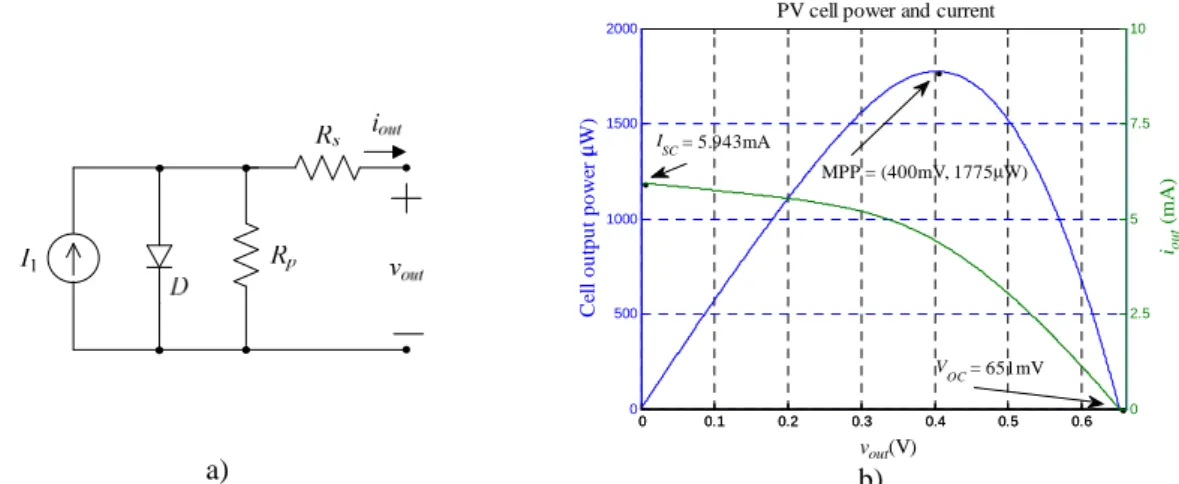
Fig. 2.19 - a) Equivalent electrical circuit of a PV cell, b) Example of typical current and power
curves, as a function of the output voltage. ... 30
Fig. 2.20 - Power spectral densities of light sources at various illuminances [80]. ... 31
Fig. 2.21 - Schematic assembly of a PEC [92]. ... 32
Fig. 2.22 - a) Wireless body area network architecture in medical healthcare system [60], b) Overall structure of a typical wireless sensor node of this WBAN [60]. ... 35
Fig. 2.23 - Conventional wired SHM system with a central monitoring station [98]. ... 39
Fig. 2.24 - Decentralized wireless SHM system employing hopping communications protocol [98]. ... 39
Fig. 2.25 - Reindeer wearing a collar containg the sensor node [99]. ... 40
Fig. 2.26 - Mounting of the sensor nodes in a) ZebraNet [93] and b) TurtleNet [93]. ... 41
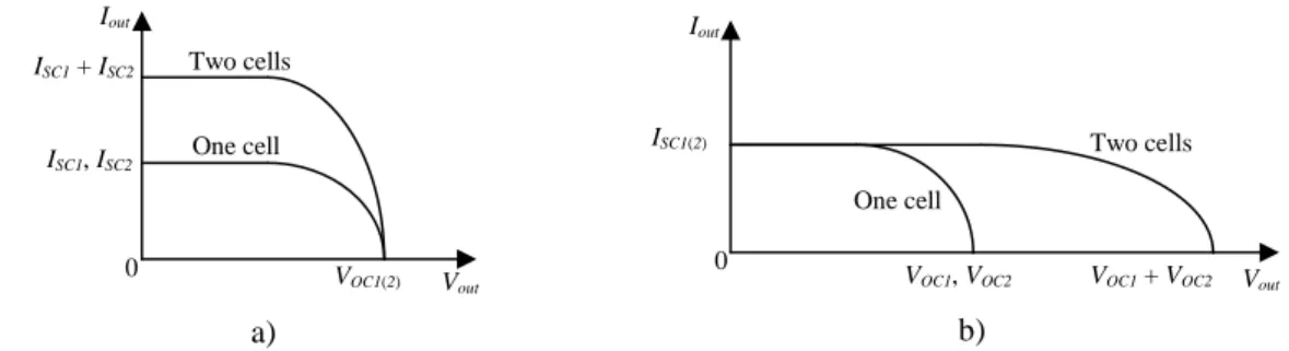
Fig. 3.1 - Connection of two identical PV cells: a) parallel; b) series. ... 44
Fig. 3.2 - Influence of irradiance and temperature on the PV cell current: a) increasing irradiance; b) increasing temperature. ... 44
Fig. 3.3 - Maximum power and fill factor. ... 45
Fig. 3.4 - Behavior of light inciding over a PV cell [101]... 46
Fig. 3.5 - Absorption coefficient for different semiconductor materials [73]. ... 47
Fig. 3.6 - Interaction of radiation with semiconductors, regarding energy bands. ... 47
Fig. 3.7 - Separation of holes and electrons in a PV cell [73]. ... 48
Fig. 3.8 - Efficiency limits of PV cells [73], considering: a) AM0 and b) AM1.5. ... 49
Fig. 3.9 - Efficiency/cost trade-off for the three generations of PV cell technologies (cost in US dollars, in 2003) [102]. ... 50
Fig. 3.10 - Monocrystalline PV module [73]. ... 51
Fig. 3.11 - Polycrystalline PV module [73]. ... 52
Fig. 3.12 - Schematic representation of an emitter wrap through PV cell [101]. ... 53
Fig. 3.13 - Cross section of a typical CdS/CdTe PV cell. ... 55
Fig. 3.14 - Cross section for a copper indium gallium diselenide PV cell. ... 56
Fig. 3.16 - Cross section of a dye sensitized PV cell [101]. ... 57
Fig. 3.17 - Structure of an organic PV cell [101]. ... 58
Fig. 3.18 - Single-walled and multi-walled carbon nano tubes [101]. ... 58
Fig. 3.19 - Timeline of PV cell energy conversion efficiencies (from the U.S. Department of Energy - National Renewable Energy Laboratory). ... 60
Fig. 3.20 - Power curve of two PV cells equivalent circuits connected in series, for different levels of illumination. ... 62
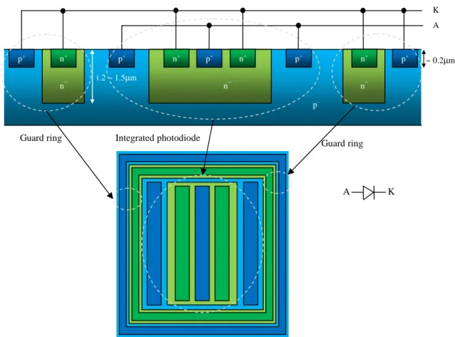
Fig. 3.21 - Layout of the integrated CMOS PV cell (left), integrated die that hosted the CMOS PV cell (middle) and photograph of the die containing the CMOS PV cell (right). ... 63
Fig. 3.22 - Simplified structure of the integrated photodiode. ... 64
Fig. 3.23 - Equivalent electrical circuit of the purpose required for the guard ring. ... 65
Fig. 3.24 - Schematic picture of the room where the indoor measurements took place. ... 68
Fig. 4.1 - Conceptual circuit for the linear series converter/regulator. ... 72
Fig. 4.2 - Conceptual circuit for the linear shunt converter/regulator. ... 73
Fig. 4.3 - Equivalent circuits for charging a) a capacitor or b) an inductor. ... 74
Fig. 4.4 - Instantaneous energy, as a function of time, for a) the capacitor and its series resistor and b) the inductor and its series resistor. ... 75
Fig. 4.5 - Boost (step-up) DC-DC voltage converter, using ideal elements. ... 76
Fig. 4.6 - Ideal voltage vL(t), as a function of time. ... 77
Fig. 4.7 - Current-fed bridge voltage converter. ... 78
Fig. 4.8 - Inverse Watkins-Johnson DC-DC voltage converter... 78
Fig. 4.9 - Buck (step-down) voltage converter. ... 79
Fig. 4.10 - Buck-Boost voltage converter. ... 80
Fig. 4.11 - Non-inverting Buck-Boost voltage converter. ... 80
Fig. 4.12 - Čuk voltage converter. ... 81
Fig. 4.13 - SEPIC voltage converter. ... 81
Fig. 4.14 - Zeta voltage converter. ... 82
Fig. 4.16 - a) Integrated metal track inductor; b) Application of integrated inductors in a layout of a monolithic converter [114]. ... 83 Fig. 4.17 - Main building blocks of a SC DC-DC voltage converter. ... 84 Fig. 4.18 - Electric model of a switched-capacitor DC-DC voltage converter. ... 85 Fig. 4.19 - Switched-capacitor DC-DC voltage step-up converter, using the ladder topology. .. 87 Fig. 4.20 - Ladder step-up converter, with lower VCR. ... 88 Fig. 4.21 - Ladder step-up converter, with a different VCR, for comparison. ... 89 Fig. 4.22 - Switched-capacitor DC-DC voltage step-up converter, using the Cockcroft-Walton topology... 90 Fig. 4.23 - Dickson charge pump step-up converter basic topology. ... 91 Fig. 4.24 - Switched-capacitor DC-DC voltage step-up converter, using the Fibonacci topology. ... 92 Fig. 4.25 - Switched-capacitor DC-DC voltage step-up converter, according to the Parallel-Series topology. ... 93 Fig. 4.26 - Switched-capacitor DC-DC voltage step-up converter, using the voltage doubler topology... 94 Fig. 4.27 - An example of a commercially available Li-on rechageable battery [132]. ... 98 Fig. 4.28 - Equivalent circuit model for a double layer capacitor. ... 98 Fig. 4.29 - Working principle of the supercapacitor [134]. ... 99 Fig. 4.30 - Charging and discharging mechanism of a supercapacitor [134]. ... 99 Fig. 4.31 - Examples of commercially available supercapacitors (50 F, 10 F and 1 F). ... 100 Fig. 4.32 - Fractional open circuit voltage relation between VOC and VMPP under various
conditions of a) illumination and b) temperature. ... 104 Fig. 5.1 - Architecture of the indoor light energy harvesting system. ... 111 Fig. 5.2 - Simplified schematic of the voltage step-up doubler converter, including the loading caused by the phase controller circuit (modeled as Cp). ... 113
Fig. 5.3 - Circuit during phase φ1. ... 113 Fig. 5.4 - Circuit during phase φ2. ... 114
Fig. 5.5 - a) Time evolution of voltages VIN and VOUT with fCLK = 459.1 kHz and RL = 16 kΩ and
b) Close-up of voltages VIN and VOUT in the steady-state zone. ... 116
Fig. 5.6 - a) Time evolution of voltages VIN and VOUT with fCLK = 200 kHz and RL = 110 kΩ and
b) Close-up of voltages VIN and VOUT in the steady-state zone. ... 117
Fig. 5.7 - A MOSFET capacitor, with explicit bottom plate parasitic capacitance. ... 118 Fig. 5.8 - Typical capacitance variation of a MOSFET capacitor of the 130 nm technology, as a function of the VGS voltage, with W = 50 µm and L = 2 µm. ... 119
Fig. 5.9 - Capacitance variation for CMOS, when using a MOSFET with W = 50 µm and L = 2 µm. ... 119 Fig. 5.10 - Variation of the bottom plate capacitance (Cp1) when using a MOSFET with W = 50 µm and L = 2 µm. ... 120 Fig. 5.11 - Ratio between the bottom and the main capacitance of a MOS capacitor like the one in Fig. 5.7, with W = 50 µm and L = 2 µm, using a 130 nm technology. ... 120 Fig. 5.12 - Schematic of the proposed step-up doubler SC converter, using MOS capacitors with charge reusing. ... 121 Fig. 5.13 - RC circuit using a transmission gate and a capacitor... 122 Fig. 5.14 - RON as function of W
-1
... 123 Fig. 5.15 - Closs as function of W. ... 123
Fig. 5.16 - State diagram of the algorithm performed by the ASM. ... 126 Fig. 5.17 - Phase controller schematic using Fractional VOC MPPT. ... 126
Fig. 5.18 - Time relation between the input and the output signals of the delay circuit. ... 127 Fig. 5.19 - Schematic of the delay circuit... 127 Fig. 5.20 - Schematic of the comparator circuits. ... 128 Fig. 5.21 - Current drawn by a logic inverter during a clock transition. During this transition, a current flows from VDD to VSS, when both transistors are ON. This draws a constant charge from VDD in each clock transition, being equivalent to a switched parasitic capacitor, whose value
varies with VDD. ... 129
Fig. 5.22 -
MPP
OUT
V as a function of RL. ... 130
Fig. 5.24 - Efficiency value, as a function of the ratio RL / RS. ... 132
Fig. 5.25 - MPP clock frequency, as a function of the switched capacitance (C1). ... 132
Fig. 5.26 - Efficiency, as a function of the switched capacitance (C1) value (the traces for the two different values of RS are overlapped). ... 133
Fig. 5.27 - Output voltages of the main and the Local Supply modules, as a function of the ratio between their respective switched capacitances. ... 135 Fig. 5.28 - Schematic of the start-up circuit. ... 136 Fig. 5.29 - An energy harvesting architecture that can host the voltage limiter described in this section (all of the modules are referenced to ground). ... 137 Fig. 5.30 - a) Available power from a prototype PV cell with 1 cm2, for different irradiance levels; b) Detail showing the power function that corresponds to the lowest irradiance level. 138 Fig. 5.31 - Architecture of the proposed voltage limiter circuit. ... 139 Fig. 5.32 - a) CMOS Voltage Reference Circuit; b) Output reference voltage (vREF), and supply
current, as a function of vdd. ... 140
Fig. 5.33 - Temperature dependence of the supply current, and generated voltage reference, for different supplying voltages, for the VRC being used. ... 140 Fig. 5.34 - Differential amplifier circuit: a) schematic, b) frequency response. ... 141 Fig. 5.35 - Small-signal model of the amplifier and the output M1 transistor. ... 141
Fig. 5.36 - Magnitude and phase functions of the feedback loop circuit of Fig. 5.31. ... 143 Fig. 5.37 - Simulated performance: a) DC sweep response; b) Dynamic transient response. .. 143 Fig. 6.1 - Entire die layout... 145 Fig. 6.2 - Layout of the switches of the SC voltage doubler: a) symbol and electric circuit; b) a single transmission gate and c) the whole set of switches that manages the step-up process in the upper branch of Fig. 5.12. ... 146 Fig. 6.3 - Layout of the MOSFET capacitors: a) concept; b) single structure; c) complete structure. ... 148 Fig. 6.4 - Logic inverter: a) logic symbol and electric circuit; b) layout. ... 149 Fig. 6.5 - AND logic gate: a) logic symbol and electric circuit; b) layout. ... 150 Fig. 6.6 - OR logic gate: a) logic symbol and electric circuit; b) layout. ... 150
Fig. 6.7 - S-R latch: a) logic symbol and internal logic circuit; b) layout. ... 151 Fig. 6.8 - Layout of the delay circuit, except for the MOSFET capacitor that defines the amount of delay. ... 151 Fig. 6.9 - a) Schematic and b) layout of the voltage divider that provides vB (95% of vin). ... 152
Fig. 6.10 - Layout of the comparator circuit. ... 153 Fig. 6.11 - Complete layout of the MPPT Fractional VOC phase controller circuit. ... 154
Fig. 6.12 - Layout of the local supply module. ... 154 Fig. 6.13 - Layout of the start-up circuit. ... 155 Fig. 6.14 - Layout of the voltage reference circuit. ... 155 Fig. 6.15 - Layout of the differential amplifier circuit. ... 156 Fig. 6.16 - Layout of the complete voltage limiter circuit. ... 156 Fig. 6.17 - Relative area occupied by each module. ... 157 Fig. 6.18 - Layout of the system and die photograph. ... 158 Fig. 6.19 - Pad ring and pin assignment. ... 158 Fig. 6.20 - Pin diagram for interconnection to the prototype PCB... 159 Fig. 6.21 - Array of buffers to drive the switches of both SC voltage doublers. ... 160 Fig. 6.22 - Layout of the set of output buffers. ... 160 Fig. 6.23 - Transient evolution of voltages vin, vdd and vout during the extracted layout simulation.
... 162 Fig. 7.1 - Establishment of initial conditions to the voltage doubler system. ... 165 Fig. 7.2 - Daughter board: a) PCB layout and bond connections; b) photograph of a fully assembled unit. ... 166 Fig. 7.3 - Complete PCB (mother board), during the tests campaign. ... 166 Fig. 7.4 - Experimental apparatus. ... 167 Fig. 7.5 - Experimental testing setup for the Start Up module. ... 167 Fig. 7.6 - Starting-up with VS = 2 V. CH1: vin, CH2: vdd, CH3: reset. ... 168
Fig. 7.8 - Starting-up with VS = 1.2 V. CH1: vin, CH2: vdd, CH3: reset, CH4: VS. vin rising is
slowed down,when compared to the previous situations. ... 169 Fig. 7.9 - Experimental setup. ... 170 Fig. 7.10 - a) Input, output and phase controller power as a function of RL for VS = 0.9 V and b)
as function of VS for RL = 13 kΩ. ... 171
Fig. 7.11 - a) Efficiency, as a function of RL, for VS = 0.9V and b) as function of VS for RL = 13 kΩ. ... 172
Fig. 7.12 - a) Local Supply output voltage (vdd), main output voltage (vout) and input voltage (vin)
as a function of RL for VS = 0.9V and b) as function of VS for RL = 13 kΩ. ... 173
Fig. 7.13 - a) Voltage conversion ratios associated to vdd and to vout, as a function of RL, for VS
= 0.9V and b) as function of VS, for RL = 13 kΩ. ... 173
Fig. 7.14 - a) Operating frequency (fCLK) as a function of RL for VS = 0.9V and b) as function of VS for RL = 13 kΩ. ... 174
Fig. 7.15 - Behavior of the MPPT circuit. CH1: phase φ1, CH2: phase φ3 CH3: vdd voltage and
CH4: vin voltage. ... 175
Fig. 7.16 - Detail allowing to see the three phase signals: CH1: phase φ1, CH2: phase φ3, CH3: phase φ2. ... 175 Fig. 7.17 - Input voltage tracking the vMPP voltage. CH1: vMPP voltage, CH2: vin voltage, CH3: vout voltage and CH4: vdd voltage ... 176
Fig. 7.18 - a) Photograph of the a-Si:H PV cells (the areas of the main and pilot PV cells are 14 cm2 and 2 cm2, respectively) and b) electrical characteristics (for minimum illumination). .... 176
Fig. 7.19 - Photograph of PV cells, daughter board and a 1 F supercapacitor, so as to show their relative size. ... 177 Fig. 7.20 - Voltage waveforms during start up for an irradiance level of a) 0.32 W/m2 and b) 4.97 W/m2. CH1: reset, CH2: vin, CH3: vdd and CH4: vout. ... 177
Fig. A.1 - Thorlabs PM100 digital power meter console and operating elements. ... A-1 Fig. A.2 - S120B silicon light sensor [170]. ... A-2 Fig. A.3 - Optical band-pass filter (centered at 450 nm). ... A-3 Fig. A.4 - Transmission functions for each of the band-pass filters used. ... A-3
Fig. B.1 - a) PV cell I(V) curve, measured in dark conditions (reverse bias corresponds to negative voltage) and b) Electrical model of the PV cell. ... B-2 Fig. B.2 - PV cell characteristic curves (measured and SPICE model) under different illumination intensities (left), zoomed for lower illumination intensities (right). ... B-2 Fig. C.1 - Simple circuit for the computation of power. ... C-1 Fig. C.2 - Switched-capacitor circuit simulated in Spectre. ... C-3 Fig. D.1 - Step-up SC voltage tripler circuit. ... D-2 Fig. D.2 - MPPT Control Module circuit. ... D-4 Fig. D.3 - Schematic of the phase generator. ... D-4 Fig. D.4 - Variable delay circuit. ... D-5 Fig. D.5 - Evolution of vin, vdd, vout and vVCO, during start-up and transient operation (illumination
of 100% and 17.5%, changing at 150 µs). ... D-6 Fig. D.6 - Evolution of vin, vdd, vout and vVCO, during start-up and transient operation (illumination
of 19% and 100%, changing at 600 µs). ... D-7 Fig. D.7 - Evolution of vin, vdd, vout and vVCO, during start-up and transient operation (Ilumination
of 100% and load resistance changing at 250 µs from 1 kΩ to 100 Ω). ... D-7 Fig. D.8 - Efficiency, circuit (input) power and load (output) power, as a function of the load resistance. ... D-8
L
IST OF
T
ABLES
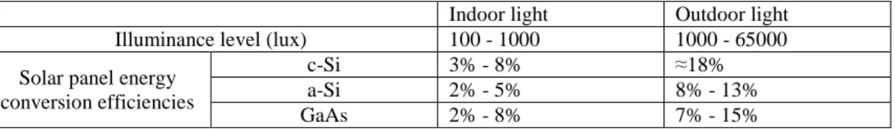
TABLE 2.1 - Demonstrated capability of some energy sources, regarding their density and performance, and examples of scenarios where to scavenge such energy sources. ... 33 TABLE 3.1 - Typical environment illuminance level and commercial available solar panel energy conversion efficiencies [80]. ... 46 TABLE 3.2 - Definition of the symbols present in Fig. 3.7, representing the energy levels. ... 49 TABLE 3.3 - Properties of some common PV cell materials. ... 56 TABLE 3.4 - PV cell electrical characteristics for different light intensities... 62 TABLE 3.5 - Absorption in Silicon, for various colors. ... 63 TABLE 3.6 - Positions where the measurements took place, referring to Fig. 3.24. ... 69 TABLE 3.7 - List of measured values, having sunny weather outside (except at 19h00m). ... 69 TABLE 3.8 - Summary of best and worst irradiance cases from the light power measurements. ... 70 TABLE 4.1 - Ideal voltage conversion ratios for switched-capacitor converters with one or two flying capacitors. ... 86 TABLE 4.2 - Comparison of recheargable battery technologies [93]. ... 97 TABLE 4.3 - Summary of the Hill Climbing algorithm. ... 105 TABLE 4.4 - Major characteristics of MPPT techniques [86]. ... 107 TABLE 5.1 - Comparison between theoretical and simulated values of VIN and VOUT. ... 117
TABLE 5.2 - Efficiency comparison of the circuit, with and without the charge reusing technique. ... 122
TABLE 6.1 - Partials and total layout areas. ... 157 TABLE 6.2 - Designation and functionality of each pin. ... 159 TABLE 7.1 - Summary of the study to determine the value of RS that yields the best efficiency.
... 171 TABLE 8.1 - Comparison with some state-of-the-art publications. ... 180
TABLE B.1 - Main properties of the constituent layers. ... B-1 TABLE B.2 - SPICE modelling parameters of the PV cell and maximum electrical power available for different illumination intensities (PV cell area = 0.49 cm2). ... B-3
TABLE C.1 - Values of the components of the circuit of Fig. C.2. ... C-3 TABLE C.2 - Results for the power computation, according to three different methods. ... C-4 TABLE D.1 - Steady-state performance of the step-up circuit. ... D-7
A
CRONYMS
a-Si:H –Hydrogenated amorphous silicon AC – Alternating current
ASM – Asynchronous state machine
BEEM – Building Energy and Environment Monitoring c-Si – Crystalline silicon
CCM – Continuous conduction mode
CMOS – Complementary Metal-Oxide-Semiconductor CPU – Central processing unit
DC – Direct current
DC-DC – Direct current to direct current DLC – Double layer capacitor
DUT – Device under test ESD – Electro static discharge EWT – Emmiter wrap through FF – Fill factor
IC – Integrated circuit I2C – Inter integrated circuit
LDO – Low drop out
MEMS – Micro electro mechanical system MFC – Microbial fuel cell
MOSFET – Metal-Oxide-Semiconductor field effect transistor MPP – Maximum power point
MPPT – Maximum power point tracking OTEC – Ocean thermal energy conversion PCB – Printed circuit board
PEC – Photosynthetic electrochemical cell PSD – Power spectral density
PV – Photovoltaic RF – Radio frequency
RFID – Radio frequency identification SLA – Sealed lead acid
SC – Switched-capacitor
SEPIC – Single-ended primary inductance converter SOI – Silicon-on-insulator
STC – Standard test conditions SHM – Structural health monitoring TEG – Thermoelectric generator UWB – Ultra wide band
VCR – Voltage conversion ratio VRC – Voltage reference circuit WBAN – Wireless body area network
WMSN – Wireless multimedia sensor network WSN – Wireless sensor network
Chapter 1
Chapter 1
Chapter 1
Chapter 1
IIII
NTRODUCTION
NTRODUCTION
NTRODUCTION
NTRODUCTION
1.1 Motivation and context
The capability of electronic circuits to obtain energy from the surrounding environment, for self powering, is an interesting feature that has gained increased attention [1], either for sensor networks [2], [3] or embedded systems [4]. This capability allows for electronic devices to operate without the need to be connected to the power grid, nor the replacement of batteries on a regular basis [1], [3], [5], [6]. This feature is especially important for sensor networks, because the remote sensor nodes can be deployed to any place where a sufficient amount of energy can be obtained from the environment. These networks can be used in a wide range of applications [3] and therefore, the design of low-cost energy harvesting devices and networks is attracting more attention [2]. This philosophy is promising to take over the powering paradigm, in opposition to traditional powering methods, involving batteries or a cord connection to the power grid. Moreover, if there is the intent of deploying a wireless sensor network (WSN) where the extension of the power grid is infeasible, or the replacement of batteries has a large cost, the use of self-powered nodes is the only option. Sensor networks that solely rely on grid connections are limited by having the sensors located close to a power outlet or from the power grid. Thus, if one wants ubiquity and pervasive operation, relying on the power grid is an evident limiting factor.
One step forward, towards unlimited sensor location, could be the use of batteries. This allows for complete freedom in the location of the sensors. However, one last obstacle remains,
which is the batteries themselves, because as their stored energy gets depleted, they need to be replaced. Eventually, this can be a problem if a large number of sensors are deployed and if they reside in places that are difficult to reach. As such, the trivial operation of battery replacement can become expensive and burdensome.
To achieve indefinite operation in inhospitable locations, the sensors must be powered in such a way that they can obtain their power directly from the surrounding environment. This kind of procedure is commonly known as energy harvesting, or energy scavenging. Besides its ubiquitous facet, energy harvesting also reveals to be interesting both in ecological and economical terms. Avoiding the need of batteries, for system main powering purposes, the sensor system will not be responsible for contributing to chemical pollution caused by disposing of batteries, or even their manufacturing, in the first place. In economical terms, not using batteries represents cost reduction both in devices and replacement procedures.
Energy harvesting systems can obtain energy from different sources: light (solar [5] or artificial [7]), electromagnetic emissions [8], mechanical movements (e.g. vibrations) [9], thermal gradients [10], etc. All of these sources share a common limitation: low energy density. This means that the electronic circuits inside the sensor node must operate using extremely low energy levels and must have efficiencies as high as possible. This poses significant design challenges. Furthermore, in many applications, the very limited available energy forces the circuits to remain in a power-down state for most of the time, until enough energy has been harvested and stored. Among all energy sources, light is the one with the highest density by volume unit, for low-power systems [5]. Moreover, photovoltaic (PV) cells are more compact devices than those that harvest energy from other sources and can be compatible with some CMOS processes [11].
In indoor environments, it can be preferable to have a sensor, or network of sensors, self supplied, in order to avoid the use of any cord connection. Using harvested energy, the costs of material like cable duct, the tangling of wires, or any other inconvenient can be avoided, in addition to having the freedom to put the nodes where exactly required. Energy can also be obtained from the light existing indoors, however, using indoor light to power an electronic application, represents an increased challenge. The levels of available light energy inside buildings are much lower than those that can be obtained outside and the available light energy in indoor environments can vary significantly, since the light from the Sun is attenuated and can be mixed with artificial light.
This thesis describes an indoor light energy harvesting system intended to power a sensor node, enabling a network similar to the one described in [12]. Although designed to cope with
indoor light levels, the system is also able to work with higher levels, making it an all-round light energy harvesting system.
A powered sensor circuit can work in an ON-OFF regime, with a low duty-cycle. When the voltage in a storage capacitor becomes larger than a certain value, the sensor circuit can be turned on, drawing current from the storage capacitor, thus reducing its voltage. This will control the maximum output voltage produced by the harvesting system.
The system that will be developed in this thesis should be fully integrated (except for the PV cells and the energy storing large value capacitor), to minimize size and cost.
The harvested energy can be stored, either in a supercapacitor [13], [14], or in a rechargeable battery [15]. The use of any of these devices enables the node to work when there is no energy available from the environment. In order to maximize the harvested power from a PV cell, it is necessary to use a DC-DC converter that can track the MPP of the PV panel. In this thesis, it is proposed to develop a MPPT DC-DC converter based on switched-capacitor (SC) networks instead of inductors [15], to reduce both the cost and volume of the system. The MPPT algorithm will be implemented in the analog domain to save power, putting aside any implementation based on a microcontroller. It is believed that by combining the experiences of specifically designing PV cells for this application, tailored to work in an indoor environment, and also designing optimized electronic circuits for energy conditioning at very low power levels, an innovative solution can be achieved.
Given that some amount of harvested energy is needed to power the control circuits, it is expectable that the efficiency, at this power level, will yield a lower value than that of a larger power application, using the same principles and algorithms. The maximum efficiencies are between 60% to 70% [13], [15]. One thing to keep in mind is that the total harvested energy must be such that it can be made useful for powering the desired application or circuit, and also to self-power the control circuitry that manages the harvester. This demand is formally stated in literature, as the Energy Neutrality [4], [16]. Generally speaking, the system will be able to work whenever it has the available energy to do it. If the system has the ability to permanently harvest enough energy from the environment, then it can permanently operate, although occasional interruptions may eventually exist. This means that interruptions will have to be tolerable, or even they can be a strategy of operation. There are a number of strategies that can be adopted, according to the type of system usage [16].
The objective of this thesis is not to develop a wireless node for a specific application, but to show that it is possible to manufacture the harvesting section, such that it can work with the available energy from its surroundings, proving that this concept can be viable. It is expected
that the developed system can be adapted to work with different types of sensors such as temperature, pressure, light, etc. If the purpose of the system is to transmit the light intensity received by the PV cells, then this information will be available from the operating frequency of the DC-DC converter. Such a node could prove its usefulness by monitoring the light conditions inside a room and, using this information, adjust the illumination to an optimal level, optimizing the electrical energy usage. This is why the system must be robust enough to operate in indoor environments, where the available light is substantially less than in outdoor scenarios [16].
Another strong motivation deals with economy and with environmental sustainability. As the overall system is intended to operate without the need of common batteries to get powered, it will pay off in the long term, since there is no need to buy additional powering components. Moreover, the power received from the surrounding environment, is zero-cost.
In addition to the economic benefit, not using batteries also means that it will not be necessary to use any process for recycling drained devices. This environmental aspect is particularly important, even though the most recent generation of batteries is progressively making use of less polluting materials. Yet a more primary consequence of avoiding battery powering, is the fact that batteries do not even need to be manufactured, in the first place.
According to the present trends, and thinking about a broader application, the node supplied by the proposed system could be a part of the Internet of Things (IoT).
1.2 Original contributions
The main contributions of the work carried out in this thesis are concentrated in the development and improvement of CMOS circuits for micro-power DC-DC converters to work with PV cells, including the implementation of MPPT algorithms using low-power controller circuits. These contributions have led to the production of various papers in conferences and journals of the area. The main contributions of this work are summarized next:
• A step-up micro-power converter for solar energy harvesting applications, based on a switched-capacitor voltage doubler architecture with MOSFET capacitors, was developed in [17]. The use of MOSFET capacitors results in an area approximately eight times smaller than when using MiM capacitors for a 0.13 µm CMOS technology. In order to compensate for the loss of efficiency, due to the larger parasitic capacitances, a charge reusing scheme is employed. An extended version of this work is provided in [18], presenting a more complete characterization and results.
• A DC-DC step-up micro-power converter, using a SC voltage tripler architecture, controlled by a MPPT based on the Fractional Open Circuit Voltage method, was developed in [19]. This circuit was designed in a 0.13 µm CMOS technology, in order to work with a a-Si PV cell. The use of this simpler method allowed for having a reduced power dissipation in the MPPT controller circuit. The system has a local power supply voltage, created using a scaled-down SC voltage tripler, controlled by the same MPPT circuit, to make the circuit robust to load and illumination variations. The SC circuits use a combination of PMOS and NMOS transistors to reduce the occupied area. The same charge reusing scheme is used just like before.
• A step-up micro-power converter using a SC voltage tripler, controlled by a MPPT circuit based on the Hill Climbing algorithm was developed in [20]. This circuit was designed in a 0.13 µm CMOS technology in order to work with an a-Si PV cell.
• An analysis of the pertinent issues about designing and developing a DC-DC converter for a low-cost, micro-power indoor light energy harvesting system, using CMOS technology, was published in [21]. From this analysis a possible solution is discussed.
• A voltage limiter circuit for indoor light energy harvesting applications was developed in [22]. This circuit ensures that, even under strong illumination, the generated voltage will not exceed the limit allowed by the technology, avoiding the degradation, or destruction, of the integrated die.
• A start-up circuit for the micro-power indoor light energy harvesting system was developed, manufactured in a 0.13 µm CMOS technology, and experimentally evaluated in [23]. This start-up circuit achieves two goals: firstly, to produce a reset signal, power-on-reset (POR), for the energy harvesting system, and secondly, to temporarily shunt the output of the PV cells to the output node of the system, which is connected to a capacitor. This capacitor is charged to a suitable value, so that a voltage step-up converter starts operating, thus increasing the output voltage to a larger value than the one provided by the PV cells.
• A micro-power light energy harvesting system for indoor environments, aimed to work under realistic indoor light intensities, was designed, manufactured and experimentally evaluated in [24]. In this system, light energy is harvested by a-Si:H PV cells, processed by a SC voltage doubler circuit with MPPT and, finally, stored in a large capacitor. The circuit occupies an area of 0.31 mm2 in a 130 nm CMOS technology. Experimental results show that the proposed system, using PV cells with an area of 14 cm2, is capable of starting-up from a 0 V condition, with an irradiance of only 0.32 W/m2. After
starting-up, the system requires an irradiance of only 0.18 W/m2 (18 µW/cm2) to remain in operation.
• A feasibility study, to check the most suitable PV technology and the levels of available indoor light energy (and their worst case), aiming to enable an indoor WSN, was made in [25]. It could be confirmed that a-Si PV cells are the most adequate for indoors.
1.3 Thesis organization
This thesis is organized as follows: Chapter 2 presents an overview about Energy Harvesting electronic systems, namely regarding energy harvestable sources and a comparison between them. Chapter 3 shows a study about PV cell technologies, an integrated CMOS PV cell that was actually implemented and a light energy availability assessment in indoor environments, in order to check the realistic conditions of the design. Chapter 4 shows the issues related to DC-DC converters, MPPT techniques and energy storing devices. In Chapter 5 it is presented the design of the proposed system. The step-up converter architecture, the design of the ASM that controls the switching and the MPPT technique than is jointly used are described. Chapter 6 presents the physical implementation of the the system, i.e. its layout in integrated circuit, using a CMOS technology. In Chapter 7, it is presented the experimental testbed, its details, and the results that were obtained from the complete manufactured prototype, composed by the integrated system and the PV cells. Finally, Chapter 8 presents the conclusions about this work, discussing the issues and the results that were shown, and future perspectives are also suggested. In Chapter 9, the complete list of literature references is given, which served to aid in the making of all of this work.
Additionally, there are four appendixes. In Appendix A, the light measuring device, used for the light availability study performed in Chapter 3, as well as its accessories, is presented so as to have an overview about it. Appendix B presents the manufacturing, characterization and analysis process of an amorphous silicon PV cell that has been specifically designed and manufactured for this work. The results about a prototype cell are presented, consisting on the parameters that can be used to model the cell for different ambient light intensities. In Appendix C it is presented a short study about how to use the waveform results given by the simulations in Spectre, so that the correct measurements about power can be computed, when dealing with SC circuits. Finally, in Appendix D, it is presented the simulated performance of a MPPT method, the Hill Climbing, firstly thought to be also included in this thesis. This inclusion did not happen but, as promising results about it had been published, it seemed worthy to briefly show the phase generator that was designed and the set of results that was achieved.
Chapter 2
Chapter 2
Chapter 2
Chapter 2
E
E
E
E
NERGY
NERGY
NERGY
NERGY
H
H
H
H
ARVESTING
ARVESTING
ARVESTING
ARVESTING
E
E
E
E
LECTRONIC
LECTRONIC
LECTRONIC
LECTRONIC
S
S
S
S
YSTEMS
YSTEMS
YSTEMS
YSTEMS
2.1 Introduction
This chapter presents a literature review about the various ambient energy sources that can be harvested and the description of some related systems. As such, Chapter 2 will provide a brief overview about each source and describe some systems that use that same energy source. This will be extended on to the domain of the wireless sensor networks and the aspects related to it, being presented some examples of energy harvesting powered WSN in different environments. A brief description of what is expected from each network and how it succeeds in harvesting the energy that enables it to work, will receive a particular focus.
Since light is the energy source being harvested, in order to power the system described in this research thesis, some more attention will be dedicated to the analysis of this source. Proceeding with this purpose, a more detailed overview about PV technologies will be given in Chapter 3. In addition, a more focused insight covering DC-DC converters, energy storing devices and MPPT techniques, will be given in Chapter 4, so as to complete the literature review opened up in the present chapter.
2.2 Available energy sources
In the surrounding environment, there are a number of possible energy sources that can be conveniently harvested, in order to power electronic applications [5]. Depending on whether a certain energy source is more abundant, that could be the preferred one.
However, another possible configuration that performs ambient energy scavenging relies on the conjunction of multiple energy sources, like in [3], [5], [10] and [26]-[29]. The latter is a highly miniaturized system, designed to have modularity, in the sense that one can add or remove IC layers, which communicate among themselves using the I2C protocol. This system occupies a volume of only 1 mm3, entering in the category of smart dust, which are wireless sensor nodes with perpetual energy harvesting. Next, Fig. 2.1 shows the evolution in terms of volume reduction that occurred over the past decades, in conformity with Bell’s law, as stated in [29]. This law is somewhat related to the well-known Moore’s law [30], although the latter may probably be reaching its limit [31].
Fig. 2.1 - Continuous down-scaling of micro-size computing systems [29].
The scavenged energy sources more commonly used are presented in this chapter and very briefly described and characterized in the following subsections, as a more detailed overview is outside the scope of this thesis. However, relevant references will be given, in order to aid in getting a broader insight about each source and related systems that are specifically designed to work with it.
2.2.1 Mechanical
Mechanical energy can be harvested from various natural sources, such as wind [32], wave motion [33], vehicle motion, or in general, any kind of vibrations or movement, namely, by resonance. There is an important issue specific to mechanical energy harvesting systems, which is the need to have rectifying circuits. As one is dealing with alternating signals, an AC to DC conversion must be carried out. The rectifiers can be passive or active. The former ones are
based on diode topologies, namely, rectifier bridges, while the latter ones employ some means of switching power conversion, as in [34].
There are several ways of converting mechanical energy into electrical energy, from which one can choose. This conversion can be done by using electromagnetic ([5] and [8]), piezoelectric [9] or electrostatic means [35]. According to [8], the most suitable materials to harvest mechanical energy are those that exploit the electromagnetic and the piezoelectric principles, possessing the highest power density, when compared to the electrostatic ones. Each of these materials has a different electrical behavior, and thus, when using any of them, a different electric interface must be used. Harvesters exploiting vibrations, presently have an efficiency ranging from 25% to 50% [36].
2.2.1.1 Electromagnetic conversion
In order to have the possibility to perform simulations, destinated to check any proof of concept, it is necessary to have a model of the harvester device. In the mechanical context, when dealing with electromagnetic conversion devices, it is usual to have finite element method (FEM) models, so as to have a suitable representation of the harvester. This model can be used in conjunction with electric circuits, in order to enable a simulation. For example, in [8], an electromagnetic energy harvester is studied using this approach. In Fig. 2.2 a), it is given an idea of how the FEM model looks like. Subsequently, this gives origin to a block diagram model at numerical level, which is shown in Fig. 2.2 b), and this one can then be translated to Spectre, for example, allowing for electric simulation. Also, it is to note in Fig. 2.2 b), how the kinematic variables are involved. Electromagnetic transducers generate a voltage offering a low impedance output.
a) b)
Fig. 2.2 - FEM model of an electromagnetic conversion device [8].
Tipically, electromagnetic conversion is used for larger power levels than the ones aimed by this thesis and, therefore, it will not be addressed further. Moreover, the cost of this type of converters is higher than for other types.
2.2.1.2 Piezoelectric conversion
There is a material, Lead Zirconia Titanate (PZT), widely used for this conversion, which is considered as the silicon counterpart of piezoelectric materials, when dealing with engineering applications, as it can be found in [1], [28] or [37].
A piezoelectric energy harvester is typically a cantilevered beam with one or two piezoceramic layers, which can vibrate in various vibration modes. The induced strain is converted into electrical charge, originating a voltage. The generated voltage is proportional to the force, and thus, to the vibration magnitude applied to the harvester. However, piezoelectric energy transducers are characterized by a high impedance output, unlike conventional voltage sources. This results in the need to use appropriate electric circuits that correctly interface with this type of transducer. The voltage generation mechanism is illustrated in Fig. 2.3.
Fig. 2.3 - Voltage generation mechanism in a piezoelectric harvester.
This kind of mechanism is bidirectional, such that by applying a voltage will result in a deformation, meaning that these materials can be used both as sensors or actuators.
The simplified electric model of a unimodal piezoelectric harvester is represented in Fig. 2.4 a).
a) b)
Fig. 2.4 - Simplified model of the piezoelectric harvester [38].
At the left hand side of Fig. 2.4 a), the mechanical part of the model is represented, where
R, L and C represent the mechanical parameters loss, mass and stiffness, respectively. The
transition from the mechanical to the electrical domain is modeled by a transformer with a ratio of n, where the conversion from stiffness to the current i is performed, instead of using the generated voltage directly. At the right hand side, i.e. in the electrical domain, Cp represents the
plate capacitance of the piezoelectric material. When at resonance, the whole circuit can be simplified to a current source in parallel with a capacitor and a resistor, in which the latter represents the losses. This model is depicted in Fig. 2.4 b). With this circuit, the MPP condition can be achieved if the load connected at the output is the conjugate of the impedance represented by Cp and Rp, i.e. the load must have an inductive component.
2.2.1.3 Electrostatic conversion
Micro electrical mechanical systems (MEMS) are well suited to collect mechanical energy. Devices using this kind of technology can be built so as to be compatible with CMOS integration, in order to lay out both the harvester and the energy processing system in the same die.
Basically, the harvester can consist of a simple variable plate-distance capacitor. The energy conversion can be achieved in two ways, either by varying the gap between the plates or varying their overlap. A simple way to illustrate this principle is by looking at Fig. 2.5, representing a rest position, from where the moving plate can suffer a translation along any of the axis, as a consequence of vibrations or any other motion.
Fig. 2.5 - Symbolic representation of the conversion mechanism using MEMS.
If this translation occurs along the y axis, the distance between plates will vary, and the capacitance will vary accordingly, in an inversely proportional way. On the other hand, if the translation occurs along the x or the z axis, the plate overlap will decrease and so will the resulting capacitance. If the capacitor is pre-charged and then kept open-circuited with a constant charge, the capacitance variation will change the voltage of the capacitor (VC) and,
consequently, the stored energy [39].
The variation of capacitance is given by the parallel plate capacitor equation,
d A
Cvar =ε0εr , (2.1)
and relies on modifying either the superposition area of the plates of the capacitor (A), the distance between plates (d) or even the dielectric constant of the insulation material between plates (εr), if a different material is inserted in between. ε0 is the dielectric constant of vacuum.
![Fig. 2.11 - Inertial generator attached to the human body [59].](https://thumb-eu.123doks.com/thumbv2/123dok_br/19199448.953176/52.892.259.641.126.364/fig-inertial-generator-attached-human-body.webp)
![Fig. 2.12 - Energy harvesting from electromagnetic waves using the human body [66].](https://thumb-eu.123doks.com/thumbv2/123dok_br/19199448.953176/55.892.275.623.130.363/fig-energy-harvesting-electromagnetic-waves-using-human-body.webp)
![Fig. 2.17 - Photovoltaic solar electricity potential of Europe and some zones of the Middle East and the North of Africa (PVGIS © European Union, 2001-2012) [74], [75]](https://thumb-eu.123doks.com/thumbv2/123dok_br/19199448.953176/59.892.255.648.747.1090/photovoltaic-electricity-potential-europe-middle-north-africa-european.webp)
![Fig. 2.22 - a) Wireless body area network architecture in medical healthcare system [60], b) Overall structure of a typical wireless sensor node of this WBAN [60]](https://thumb-eu.123doks.com/thumbv2/123dok_br/19199448.953176/67.892.168.709.408.632/wireless-network-architecture-medical-healthcare-overall-structure-wireless.webp)
![Fig. 3.9 - Efficiency/cost trade-off for the three generations of PV cell technologies (cost in US dollars, in 2003) [102]](https://thumb-eu.123doks.com/thumbv2/123dok_br/19199448.953176/82.892.265.626.495.759/fig-efficiency-cost-trade-generations-cell-technologies-dollars.webp)