Light-emitting thin-film field-effect transistors
8
0
0
Texto
(2) 374. P. STALLINGA, H.L. GOMES. across the device and no barriers exist at the contacts. No effects of the contacts are observed in MOS-FETs. In contrast, the source and drain contacts in TFTs are normally made of metal. Severe rectifying contact effects might be expected, similar to Schottky diodes. Recently, we have developed a model for the contacts in FETs, which explains how such metallic contacts cause a potential in the channel and the formation of a tiny residual barrier [7]. 2) The active layer in TFTs, as the name implies, is very thin. Recent studies of organic materials have shown that a single monolayer of active material is enough to make the device fully functional [8, 9]. Further layers on top of the first can serve as impurity diffusion barriers or help the mechanical stability and/or crystallinity, or prevent the formation of islands and interrupted current paths in the devices. It is only a continuous coverage of the insulator that is needed for the devices to work properly. 3) Most TFTs, especially the ones made of organic material, commonly work in accumulation. This means that the carriers of the channel are of the same type as the carriers in the material in its bulk form. MOS-FETs, on the other hand, work in inversion. The last two items cause severe doubts as to the validity of the application of MOS-FET models to TFTs. The band bending needed to drive the active layer into conduction by the formation of a free-charge channel is caused by the charges themselves, via Poisson’s equation; the potential is the double integral of charge where the integration is performed in the direction perpendicular to the interface. For films that are extremely thin, this integral is vanishing, yet they work. Still more severe is the problem with the formation of an accumulation channel in this model, even if the layers are thick. For such a channel there are no electronic states available to store immobile charge of the correct sign needed for the band bending. The only charge of correct sign is then the free charge which without any way to resist the field of the gate, would move towards the interface, only being stopped by the energetic barrier of the insulator. As an example, in a p-type accumulation FET the only electronic states, apart from those of the valence band, are acceptors, and these can only be negatively ionized, inappropriate for the building of the band bending of correct sign. In conclusion, in either TFTs or accumulation MOS-FETs, the whole induced charge is necessarily close to the interface and the MOS-FET model is inadequate.. 2. New model We developed a model [10, 11] for the description of an accumulation type TFT. It is based on the assumption that whole free charge is close to the interface. As a consequence, the entire charge induced feels only the insulator capacitance Cox = εox /dox , where εox is the permittivity of the insulator and dox its thickness. This then results in a simple charge-voltage relation, which at any place in the channel x is given by. ρ ( x ) = V ( x ) – V g C ox. (1).
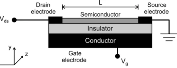
(3) Light-emitting thin-film field-effect transistors. 375. Fig. 1. Cross-section of a TFT consistent with the nomenclature used in the current work.. with ρ (x) and V (x) the local per-area charge density and potential at a point x in the channel, respectively (see Fig. 1 for a cross-section of a TFT and a description of the parameters used in this work), Vg – the tension at the gate. For a simple model, this charge is composed of only free holes p. Note the units of this charge density is coulomb per square meter because the active layer is treated as two-dimensional. The current Ix at a point x is proportional to the local charge density, the local field and the charge mobility µ p, multiplied by the channel width W and thus we get the following differential equations: C ox V ( x ) – V g p ( x ) = -----------------------------------------q. (2). ∂V ( x ) I x ( x ) = qWp ( x ) µ p -----------------∂x. (3). where q is the elementary charge. With boundary conditions V (0) = 0, V (L) = Vds the external voltage, and Ix(x) = Ids the external measured current for all x, the solution of the above set equations is: W 1 2 I ds = --------C ox µ p V g V ds – ----- V ds L 2. (4). where Vds and Vg are both negative for a p-channel. Figure 2 shows simulations of the I-V and transfer curves. This is exactly equal to the behavior of p-type inversion -channel MOS-FET which explains why the MOS-FET model is persistently used in literature to describe TFTs; empirically, the curves are the same. In a full article [10, 11], to be published elsewhere, we give a more detailed description of the TFT model. For example, we show that traps cause the existence of a threshold voltage, power-law transfer curves, temperature activation of current and mobility, and the observation of the Meyer–Neldel rule (which tells that the activation energy depends on bias). In summary, we found that the model explains all our data of TFTs of organic materials, where the MOS-FET model fails or needs ad-hoc additions and parameters. The model works equally well for ambipolar devices. In the preceding text it was assumed that the mobility of the free electrons was so low that they never contribute.
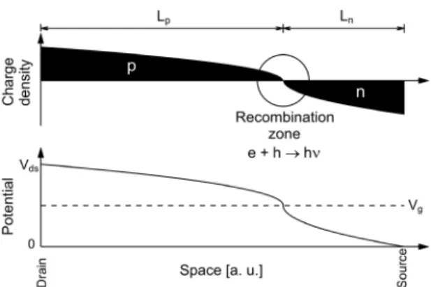
(4) 376. P. STALLINGA, H.L. GOMES. a. b. Fig. 2. I-V curves (Ids vs. Vds) of an ideal thin-film FET resulting from Eq. (4) (thin lines) – a; transfer curves – b. The parameters are: µ = 3×10⁻⁴ cm2/Vs, Cox = 160 µF/m2, W = 1 cm, L = 10 µm, Vt = 0. Absolute values for current and voltage. Thick lines indicate the saturation regime.. to current, µn ≈ 0, even when electrons are injected into the conduction band. For this reason, when the gate bias is positive, and no free holes but only immobile electrons, exist at any place in space, no current is possible. We will now extend the idea and show what happens when electrons have a mobility comparable to that of holes. When ignoring the subthreshold (“minority carrier”) concentrations, the basic equations are replaced by: V ( x ) > Vg :. C ox V ( x ) – V g p ( x ) = ----------------------------------------q. (5). n(x) = 0 V ( x ) < Vg :. p(x) = 0 – C ox V ( x ) – V g n ( x ) = -------------------------------------------q. (6). and dV ( x ) I x ( x ) = qW p ( x ) µ p + n ( x ) µ n -----------------dx. (7). with µ p and µ n being the field-effect mobility of holes and electrons, respectively. When the gate bias is outside the range 0–Vds it has only one type of charge throughout the device and it can be treated as a p-channel or n-channel device. A more complicated case exists when the gate bias is in the range between the drain and source potential. In this case, there exists a region of length Ln with free electrons and a region of length Lp with free holes, see Fig. 3. At the junction point the potential is equal to.
(5) Light-emitting thin-film field-effect transistors. 377. Fig. 3. Charge distribution and potential in an ambipolar TFT when the gate bias is in between the drain and the source bias. For such conditions, the device is in a dual-injection regime, with a zone of positive and a zone of negative charge. In this example: µ p = 2µ n, Vds > 0 and Vg = Vds/2.. the gate-bias. Diffusion carries the electrons to the hole channel and vice versa. Therefore there exists a zone of length approximately equal to the sum of the individual diffusion lengths of holes and electrons where both these carriers coexist and where the recombination takes place and light originates. When we assume that at this junction the electron-hole recombination is not the limiting factor, we can treat the electron channel and hole channel regions as an FET in saturation. Then, demanding equal current in both regions (e.g., for Vds > 0) and using the fact that the total length must be equal to the channel length Lp + Ln = L, we find for Vds > 0 2 1 W 2 I ds = ------ ------- C ox µ n V g + µ p V ds – V g 2 L. (8). In the same way we can find for Vds < 0 2 1 W 2 I ds = – ------ ------- C ox µ n V d s – V g + µ p V g 2 L. (9). Figure 4 shows the transfer curves of ambipolar devices. The thick parts of the curves indicate the dual-injection regime. Such curves can serve as rapid evaluation tools. The minimum of a particular transfer curve can be found by taking the derivative of Eqs. (8) or (9) and at the minimum this is zero:. µp. mi n. Vg. V ds < 0. = ---------------------- V ds µp + µn. V ds > 0. = ---------------------- V ds µp + µn. µn. mi n. Vg. (10). (11).
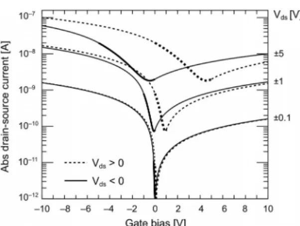
(6) 378. P. STALLINGA, H.L. GOMES. Fig. 4. Transfer functions for ambipolar devices for drain-source biases as indicated. The thick parts of the curves indicate the dual injection regime as shown in Fig. 3. The solid curves are for negative drain-source biases whereas the dashed curves are for positive Vds (µ n = 0.1µ p).. The ratio of the positions of the minima in positive and negative bias thus directly yields the ratio of electron and hole mobility. The device described above is based on a material that is ambipolar itself, with high values for both the electron and hole mobility. In other geometries, this limitation can be overcome. In one design, two layers are deposited, one on top of the other. One layer has high electron mobility while the other is a good hole conductor. The model described above is adequate for this geometry with a small modification. For the layer closest to the interface, the insulator capacitance is Cox. For the top layer, however, the effective capacitance is reduced and is a series capacitance of the insulator and the first layer. This capacitance has to substitute Cox in Eqs. (5) or (6), depending on which layer is the top one. A slightly more complicated solution compared to Eqs. (8) and (9) is then found. Care has to be taken to include in the design a barrier for carriers of the top layer to be prevented from moving into the bottom layer. This determines the preferred stacking order of the materials. Another geometry is a deposition of parallel or interdigitated tracks of hole and electron transport material. The fabrication of this device is rather complicated, but the above theory will work without modifications. There are many reports in literature about ambipolar TFTs. At the first sight, the curves presented here are slightly different from curves reported in literature. It has to be born in mind that the simulations assume a zero threshold voltage for both the n- and p-channel. In reality, this threshold voltage can be substantial and this distorts the figures. In the first instance, it will shift the transfer curves of Fig. 4 by the threshold voltage if Vt for hole conduction and electron-conduction are equal. The picture becomes more complicated when they are different. Even worse is the case when the threshold voltage is changing during the measurements, in so-called stressing [12]. This also allows for the n- and p-channel threshold voltages to be separated when the stressing is significant in the time scale of the measurements..
(7) Light-emitting thin-film field-effect transistors. 379. Fig. 5. Cross-section of a molecular FET consisting of three molecules with different electrical properties. Most organic materials are insulating and can serve as separator material. This is then sandwiched between a metallic molecule and a semiconducting molecule with an intermediate LUMO-HOMO energy separation, like most conjugated organic materials. The resulting device will behave as an accumulation type FET without restrictions. The symbols S, D and G denominate the source, drain and gate of the final transistor, respectively.. The new model presented has consequences for the lower limit of the size of the devices. In comparison, the principle of operation in standard MOS-FET devices is based on band bending caused by space charge. The extent of this space charge zone is a reciprocal square-root function of the donor density [5]. Therefore, there is a direct link between the acceptor concentration and the spatial extent Y of the band bending zone. A typical device of silicon (Eg = 1.15 eV, ε = 11.9 times the permittivity of vacuum), with a doping density ND = 1×1016 cm3, needs a thickness of at least Y = 400 nm and this is then a lower limit to the size of a device. With heavier doping, the limit can be somewhat lowered. Because the presented model does not need band bendings, there are no lower limits as to the dimensions of the devices, and the devices can therefore be as thin as desired. For example, a device with an insulator capacitance density of Cox = 100 µF/m2 with 1 V bias has a per-area charge density of 0.1 mC/m2. With a density-of-states of NV = 1.04×1019 cm–3 this can theoretically fit in less than 1 Å height. Thus, a device can be constructed of three molecules. The middle molecule should be an insulating one with a high LUMO-HOMO (lowest-unoccupied and highest-occupied molecular orbits, respectively) separation, representing a large bandgap, comparable in function to silicon oxide. On one side of this insulator there should be a “metallic” molecule, without a bandgap, taking the role of the gate, and on the other side a semiconductor, this material being the most critical in the device. An organic conjugated material can be used, and it has been shown that, for instance, a DNA molecule can serve as active layer [13]. Figure 5 gives a schematic representation of this molecular electronic device.. 3. Conclusions In conclusion, we presented a new model for light-emitting thin-film transistors where the current is only occurring in the first monolayer of the semiconductor and no space charge and band bendings exist. This model is applicable to FETs working in.
(8) 380. P. STALLINGA, H.L. GOMES. accumulation, for instance, most (organic) TFTs. We show how with the use of this model it is possible to fabricate ultra-small devices. Acknowledgements – This work was sponsored by project POCTI/FAT/47956/2002 and POSC research unit CEOT.. References [1] BABEL A., WIND J.D., JENEKHE S.A., Ambipolar charge transport in air-stable polymer blend thin-film transistors, Advanced Functional Materials 14(9), 2004, pp. 891–8. [2] YASUDA T., GOTO T., FUJITA K., TSUTSUI T., Ambipolar pentacene field-effect transistors with calcium source-drain electrodes, Applied Physics Letters 85(11), 2004, pp. 2098–100. [3] SIRRINGHAUS H., An equal-opportunity conductor, Nature Materials 2(10), 2003, pp. 641–2. [4] ROST C., KARG S., RIESS W., LOI M.A., MURGIA M., MUCCINI M., Ambipolar light-emitting organic field-effect transistor, Applied Physics Letters 85(9), 2004, pp. 1613–5. [5] SZE S.M., Physics of Semiconductor Devices, 2nd ed., Wiley 1981. [6] HOROWITZ G., Organic field-effect transistors, Advanced Materials 10(5), 1998, pp. 365–77. [7] STALLINGA P., GOMES H.L., to be published. [8] MUCK T., WAGNER V., BASS U., LEUFGEN M., GEURTS J., MOLENKAMP L.W., In situ electrical characterization of DH4T field-effect transistors, Synthetic Metals 146(3), 2004, pp. 317–20. [9] DINELLI F., MURGIA M., LEVY P., CAVALLINI M., BISCARINI F., DE LEEUW D.M., Spatially correlated charge transport in organic thin film transistors, Physical Review Letters 92(11), 2004, pp. 116802/1–4. [10] STALLINGA P., GOMES H.L., accepted for publication in Synthetic Metals (2006). [11] STALLINGA P., GOMES H.L., accepted for publication in Synthetic Metals (2006). [12] GOMES H.L., STALLINGA P., DINELLL F., MURGIA M., BISCARINI F., DE LEEUW D.M., MUCK T., GEURTS J., MOLENKAMP L.W., WAGNER V., Bias-induced threshold voltages shifts in thin-film organic transistors, Applied Physics Letters 84(16), 2004, pp. 3184–6. [13] WATANABE H., SHIMOTANI K., SHIGEMATU T., MANABE C., Electric measurements of nano-scaled devices, Thin Solid Films 438–439, 2003, pp. 462–6.. Received December 15, 2005.
(9)
Imagem

+2

Documentos relacionados
Consistent with the fact that the rate-limiting step was shifted at the level of the glycerol efflux, overexpression of FPS1 encoding the major glycerol facilitator ( Luyten et al.,
De acordo com os limites estabelecidos na Instrução Normativa n.51 (BRASIL 2002), as amostras de leite analisadas, pasteurizado tipo C padronizado, da região de
Investigamos como a América aparece em suas enunciações para identificarmos as razões que levaram ambos os autores a discursarem de maneira a abranger boa parte
A pesquisa que ora apresento, cuja base prática resultou na montagem do espetáculo “...é o que fica.”, investigou a presença dos modos de criação cênica a partir de
Including a MapReduce programming primitive in Prolog has three major benefits: (i) to make available a high-level abstract construct which implements the MapReduce functional
[4, 15], in order to do that the reaction time had to be decreased and the sample had to be submitted to a more intensive cleaning with toluene in order to remove the excess of
Cabe ao Farmacêutico perceber quais são as necessidades dos utentes e se a medicação é adequada à patologia em causa, pois muitas das vezes é o Farmacêutico que
Trata-se de um estudo ecológico de séries temporais, de caráter exploratório, com dados de 61.412 mil internações por ATT em população residente no Estado de
