Parylene C as substrate, dielectric and encapsulation for flexible electronics applications 1
Inês de Oliveira Martins
Licenciada em Ciências de Engenharia de Micro e Na notecnologias
Parylene C as s ubs trate, dielectric and
encaps u lation for flexible ele ctronics applications
Dissertação para obtenção do Grau de Mestre emEngenharia de Micro e Nanotecnologias
Orie nta dora : Profe ssora Doutora Joa na Dória Va z P into,
Profe ssora Auxiliar, FCT-UNL
J úri:
Pres idente : Profes s or Doutor Rodrigo Fernão Pa iva Martins Argue nte: Profes s or Doutor Henrique Le one l Gomes
Vogal: Profes s ora Doutora J oana Dória Va z Pinto
Parylene C as substrate, dielectric and encapsulation for flexible electronics applications iii Parylene C as substrate, dielectric and encapsulation for flexible electronics applications
Copyright © Inês de Oliveira Martins, Faculdade de Ciências e Tecnologia, Universidade Nova de Lisboa.
Parylene C as substrate, dielectric and encapsulation for flexible electronics applications v
“Never let your fear decide your fate.”
Parylene C as substrate, dielectric and encapsulation for flexible electronics applications vii
Acknowledgement
Parece que chegou ao fim mais uma longa etapa que só se tornou possível devido ao contributo de pessoas com quem convivi ao longo destes anos e particularmente ao longo destes meses.
Em primeiro lugar quero agradecer à minha instituição, a Faculdade de Ciências e Tecnologia da Universidade Nova de Lisboa, e ao Departamento de Ciências dos Materiais que me fizeram crescer como pessoa e como estudante.
Queria também agradecer ao professor Rodrigo Martins e à professora Elvira Fortunato pois sem eles não existiria a oportunidade de me formar no curso de Engenharia de Micro e Nanotecnologias, nem a possibilidade de desenvolver os meus conhecimentos num local tão privilegiado como o CENIMAT.
Um especial agradecimento à minha orientador Joana Pinto por toda a dedicação, paciência e orientação ao longo da realização desta tese. É com toda a certeza que digo que não é possível existir melhor orientadora. Obrigada pela motivação, pela confiança e por sempre acreditar em mim.
Gostaria também de agradecer ao grupo de trabalho, nomeadamente ao professor Pedro Barquinha, professora Rita Branquinho e professor Rui Igreja por todas as opiniões e criticas que contribuíram para a concretização deste trabalho.
A toda a equipa do CENIMAT pelo bom ambiente e espirito de entreajuda. Aos meus colegas do open space por toda a diversão e brincadeira, bom ambiente e festa, mas também pela ajuda que sempre disponibilizaram ao longo dos meses. Um especial agradecimento ao Emanuel por estar sempre disponível a ajudar e tirar qualquer duvida.
Aos meus compinchas do almoço Cátia, Tiggus e Pinela, por ouvirem as minhas queixas e lamurias. Um agradecimento muito especial à Cátia que sempre me acompanhou e ajudou ao longo deste percurso sempre com uma musiquinha para cantar.
À minha família da Caparica, Chico, Xana, Alex, Jolu, Crespo e David obrigado por estes 5 anos, que venham muitos mais.
Às minhas grandes amigas piteckas, que apesar de longe estão sempre presentes, em particular à Rita e à Ticas pela amizade e por me compreenderem sempre que reclamava. Aos meus amigos de infância, Hugo, Nani e Mónica por todo apoio e amizade ao longo da vida.
Obrigada Viorel por todo o apoio e força especialmente durante este semestre, sei que consigo ser muito chata, mas tu aturas-me sempre, obrigada por isso.
Parylene C as substrate, dielectric and encapsulation for flexible electronics applications ix
Abstract
Flexible electronics have received a lot of attention in recent days due to the several possible applications that can be envised. The aim of this work was to produce thin film transistors (TFTs) fully conformal and flexible suitable for skin electronics applications. For that, parylene C was used as a flexible substrate and, since parylene has good electrical properties, being a good insulator, it was also used as dielectric and encapsulation layers of the TFTs, combining all parylene C qualities in one device. Parylene is a semicrystalline polymer, so to study how some parameters such as thickness and temperature influence the crystallinity, X-ray diffraction (XRD) analysis was performed.
For parylene as TFT dielectric layer it was concluded that the optimum thickness was between 200 and 300 nm, reaching TFT mobilities between 10 and 15 cm2V-1s-1, ON/OFF ratio higher than 106 and
low leakage current smaller than 10-10 A. The use of parylene as a encapsulation layer improves the
behavior of the TFTs with more stability and less variability between similar devices. The use of parylene as a substrate does not affect greatly the performance of the devices being a promising material for electronic skin due to its conformal properties. Finally, the peel off of the films was studied and it was concluded that the better option consists in depositing a polyvinyl alcohol (PVA) film at the glass carrier before the parylene substrate deposition.
Parylene C as substrate, dielectric and encapsulation for flexible electronics applications xi
Resumo
A eletrónica flexível tem recebido muita atenção nos últimos anos devido às possíveis aplicações que permite antever. O objetivo deste trabalho foi criar transístores de filme fino (TFTs) completamente conformáveis e flexíveis aptos para aplicações do tipo skin electronics. Para isso utilizou-se parileno C como substrato flexível e, uma vez que o parileno tem boas propriedades elétricas sendo um bom isolante, foi também utilizado como camada dielétrica do TFT e como camada de passivação, combinando assim todas as qualidades do parileno C num único dispositivo.
O parileno é um polímero semicristalino, e foram feitas análises de difração de Raios-X (DRX) de forma a avaliar como certos parâmetros influenciam a cristalinidade, tais como temperatura e a espessura do filme.
Para a camada dielétrica do TFT obteve-se uma espessura ótima entre os 200 e 300 nm, atingindo-se mobilidades nos TFTs entre 10 e 15 cm2V-1s-1, razões On/Off superiores a 106 e correntes de fuga
reduzidas, inferiores a 10-10 A. Como camada de passivação o parileno mostrou melhorar o
comportamento dos TFTs e quando usado como substrato não interfere no desempenho dos dispositivos sendo um material promissor para dispositivos do tipo pele eletrónica. Por fim fizeram-se testes de descolagem dos filmes de parileno e concluiu-se que a melhor opção consiste em depositar uma camada de álcool polivinílico (PVA) no vidro de suporte antes da deposição do parileno como substrato.
Parylene C as substrate, dielectric and encapsulation for flexible electronics applications xiii
Abbreviations
CENIMAT Centro de Investigação de Materiais CVD Chemical Vapor Deposition
e-skin Electronic skin FET Field Effect Transistor IGZO Indium Gallium Zinc Oxide MIM Metal-Insulator-Metal PPX Poly(para-xylylenes) PVA Polyvinyl Alcohol
RFID Radio-Frequency Identification SEM Scanning Electron Microscopy TFT Thin Film Transistor
UV Ultraviolet
Parylene C as substrate, dielectric and encapsulation for flexible electronics applications xv
Symbols
ε0 Vacuum permittivity
κ Dielectric constant
µFE Field-effect mobility
µSat Saturation mobility
ρ Resistivity
A Area
C Capacitance
C/A Capacitance per unit area
Ci Gate dielectric capacitance per unit area
d Dielectric thickness
f Frequency
gm Transconductance
I Current
IDS Drain to source current
IG Leakage/gate current
ISat Saturation current
J Current density
L Channel length
m Mass
ON/OFF Ratio between the maximum of IDS and the minimum
S Subthreshold slope
V Voltage
VDS Drain to source potential
VGS Gate voltage
Parylene C as substrate, dielectric and encapsulation for flexible electronics applications xvi
VT Threshold voltage
Parylene C as substrate, dielectric and encapsulation for flexible electronics applications xvii
Table of Contents
Parylene C as substrate, dielectric and encapsulation for flexible electronics applications xix
List of Figures
Figure 1.1-Three most common parylene types. Adapted from [17] ... 2
Figure 1.2 -Different TFT structures. From [28]... 3
Figure 1.3 – Typical TFT curves. a) transfer curve, b) output curve ... 5
Figure 2.1 - Parylene deposition system. From [41]. ... 8
Figure 3.1 - Calibration of the parylene deposition system. Relation between the dimer mass and the parylene film thickness ... 9
Figure 3.2 - Diffractogram from XRD analysis for different parylene thicknesses ... 10
Figure 3.3 –In situ XRD analysis with temperature. a) Diffractograms for different temperatures. b) Dependence with temperature of the intensity and width of the parylene peak. c) Dependence with temperature of the angle 2θ of the parylene peak ... 11
Figure 3.4 - Stress/strain curve of parylene ... 12
Figure 3.5 – Study of the electrical properties of the MIM capacitors. a) Relation between capacitance and area for different parylene thicknesses. b) Capacitance per unit area-thickness for different sizes capacitors. c) Influence of electric field on the current density for the 1.5×1.5 mm2 size capacitor with 0.96µm thick parylene and photograph of MIM capacitors fabricated. d) Relation between capacitance per unit area and frequency for 1.5×1.5 mm2 size capacitor with 0.96µm thick parylene. ... 14
Figure 3.6 – Transfer curves of the TFTs using different dielectric thicknesses; a) corresponding to 0.2g of dimer. b) corresponding to 0.5g of dimer. c) corresponding to 1.0g of dimer. d) corresponding to 1.5g of dimer ... 17
Figure 3.7- Electrical characterization of the TFTs with a dielectric thickness corresponding to 0.3g dimer mass. a) Output curve. b) Transfer curve. ... 18
Figure 3.8- Transfer curves of TFTs with VDS=7V, from UV-ozone tests performed before parylene deposition with different exposure times: a) no exposure; b) 5 min; c) 15 min and d) 30 min. ... 19
Parylene C as substrate, dielectric and encapsulation for flexible electronics applications xx
[43], c) Bottom gate configuration characterized after one month, d) Top gate configuration
characterized after one month. ... 21
Figure 3.10 – Bottom gate samples after the high temperature annealing, formation of the bubbles on the contacts and channel. ... 22
Figure 3.11 – Electrical characterization of TFTs, a) without encapsulation layers, b) after the deposition of parylene encapsulation layer ... 23
Figure 3.12 – Transfer curves of a TFT with a VDS=7V. a) on corning glass substrate, b) on parylene substrate. ... 24
Figure 3.13- Substrate cracks due to heating. a) Optical microscope image of the edge of the substrate. b) SEM image of the parylene substrate among the TFTs ... 25
Figure 3.14 – Photograph of the peel-off method with the Kapton tape. ... 26
Figure 3.15- Peel-off of a sample with a PVA film under the parylene C, different phases of the peel-off. ... 26
Figure 3.16 – Parylene film with 1 µm thick as substrate with TFTs. ... 27
Figure 3.17 - TFT’s schematic with the thickness of all parylene layers defined. ... 27
Figure 3.18 – Electrical characterization of TFTs, a) before the peel-off of the substrate, b) after the peel-off. ... 28
FigureA.0.1 – Schematic of the several depositions during the TFTs fabrication ... 35
Figure B.0.1 - Shadow mask used to produce the MIM capacitors. ... 37
Parylene C as substrate, dielectric and encapsulation for flexible electronics applications xxi
List of Tables
Table 3.1- Electrical characterization of MIM capacitors with five different insulator thicknesses, for the capacitor size 1.5×1.5 mm2 ... 13
Table 3.2 – Electrical characterization of TFTs with different parylene dimer masses and consequently different dielectric thicknesses. ... 16
Table 3.3 – Electrical characterization of TFTs with different UV-ozone exposure times. ... 19 Table 3.4 - Electrical characterization of the bottom gate sample one month after the production . 21 Table 3.5 – Parameters extracted from the electrical characterization of the TFTs before and after the encapsulation ... 23
Table 3.6 - Parameters extracted from the electrical characterization of the TFTs on corning glass and on parylene C substrate ... 24
Table C.1 – Transfer curves of the TFTs produced for the thickness study of the dielectric layer, on the left the best TFT for each thickness and each size, on the right all the TFTs for each condition. .. 39
Parylene C as substrate, dielectric and encapsulation for flexible electronics applications xxiii
Motivation and Objectives
Parylene C is a polymer with very well-known properties and used mainly as a good encapsulation material especially for biomedical applications since it is an inert biocompatible and biostable material, and is also a good barrier to the diffusion of atmospheric species [1–4].
In the past years it has received attention as a gate dielectric for thin-film transistors (TFTs), mainly in organic devices due to parylene C good electrical properties [5–9].
Other properties of interest of parylene C is the flexibility, bendability and conformability. These characteristics allows it to be used as substrate in numerous applications, for example large-area flexible displays, RFID tags and flexible sensors that can be applied in wearable electronics, smart labels or electronic skin [10–12].
For flexible electronics, normally organic layer materials are used not just for the dielectric but also for the substrate and active layers due to interface and compatibility between the layers [2, 5, 7, 8].
Even though organic TFTs are receiving a lot of attention they have some flaws mostly because of the organic semiconductor used, such as their low mobility and instability. These can be overcome by combining inorganic semiconductors, like mixed metal oxides such as In-Ga-Zn-O (IGZO) having high mobility, and organic insulators making an hybrid device [13].
The main purpose of this dissertation is to combine all the advantages of parylene C in one device (in this case a TFT) using IGZO as the semiconductor and parylene C layers as the substrate, the dielectric and the encapsulation layer. For that, a study of the electrical and physical properties of the material will be conducted, and trough MIM capacitor structures, the electrical properties such as dielectric capacitance and current density will be studied.
Parylene C as substrate, dielectric and encapsulation for flexible electronics applications 1
1.
Introduction
1.1
Flexible electronics
Flexible electronic circuits, using thin-film transistors (TFTs) have received increasing attention in the last decades once devices started to be produced on polymeric substrates at very low cost [12].
Flexible can mean many qualities: bendable, conformally shaped, elastic, lightweight, roll-to-roll manufacturable, and area [12]. These qualities allow various possible applications, such as large-area flexible displays, RFID tags, wearable electronics, and biomedical devices for example e-skin sensors. These applications are not possible with wafer-based electronics because silicon based technology are rigid and fragile, require sophisticated microfabrication techniques such as high temperature and high vacuum processing steps. In addition the cost of production is very high so it is normally applied to small area devices [2, 5, 10, 13, 14].
The flexibility of the devices does not rely only on the substrate since all the materials used to fabricate the device must comply with bending to some degree without losing their function [12].
There are two approaches to make flexible electronics, one is to transfer the completed circuit to a flexible substrate and the other is to fabricate the devices or circuits directly on the flexible substrate [12, 14].
The first flexible device reported in 1960s was a solar cell, and the approach used to produce the solar cell was the transfer technique: the solar cell was fabricated on a Si wafer that were first thinned to 100 µm and then they were transferred and bonded to a flexible substrate [14, 15].
In this dissertation, the method that will be used to fabricate the TFTs will be the second approach producing the device directly on the parylene C substrate. This approach requires more attention because the processing steps need to be compatible with the polymer substrate, as an example the process temperatures need to be low so it can be tolerated by the polymer [12, 14].
The substrate needs to be bonded to a rigid carrier such as glass or silicon wafer during the processing because organic polymers typically have high coefficient of thermal expansion and low dimensional stability, and this strategy will improve the dimensional stability [16]. Other reason for the need of the rigid carrier is the thin thicknesses that are desired for some applications.
Parylene C as substrate, dielectric and encapsulation for flexible electronics applications 2
1.2
Parylene
Parylene is a common generic name for poly(para-xylylenes) polymers also known as PPX, and are part of a family of semi-crystalline thermoplastic polymers [17, 18].Parylene consists of a linear chain of benzene rings with two methylene groups replacing 2 hydrogen atoms on opposite sides of the benzene ring serving as coupling links for the polymer [19].
There are over 20 parylene derivatives depending on the molecules that replace some of the hydrogen atoms but the three most common types of parylenes, are presented on Figure 1.1, they are parylene D with two chlorines on the benzene ring, parylene C with one chlorine on the benzene ring and parylene N with no chlorines on the benzene ring [17, 20].
Parylene N Parylene C Parylene D
Figure 1.1-Three most common parylene types. Adapted from [17]
The discovery of the parylene polymer was made by Michael Szwarc in 1947 as one of the thermal decomposition products of the common solvent p-xylene at temperatures over 1000°C. Summing up, Michael Szwarc deduced that it had been formed p-xylylene by the polymerization of p-xylene [21, 22]. The reaction done by Szwarc had a small reaction yield, and in 1960s William Gorham developed an more efficient alternative to the Szwarc method that involved the pyrolysis of the dimer form of the material [17, 22].
Nowadays the method in use is the Gorham vapor-deposition process, being the method used in this dissertation to deposit parylene C, that is the most popular type of parylene due to his properties and cost.
The deposition of parylene allows coating any geometry with a uniform and conformal thickness, making parylene C a pin hole free material [14].
Physically, parylene C has a lot of similarities with most of the polymers, it is lightweight, flexible, mechanically strong and optically transparent [9, 14, 18]. Additionally, it is a good barrier to moisture and gases due to his low permeability, it has good dielectric properties and does not react with most chemicals [18, 23, 24]. Another advantage of parylene C is its biostable and biocompatible characteristics [24, 25].
Parylene C as substrate, dielectric and encapsulation for flexible electronics applications 3
of the TFTs and the mechanical properties such as flexibility and high mechanical strength for substrate applications.
1.3
Operational principle of TFT
A TFT is a field effect transistor (FET) with three terminals the gate, source and drain. It has a semiconductor layer between the source and the drain electrodes and a dielectric placed between the gate electrode and the semiconductor [26]. The gate controls the current that flows between the source and the drain depending on the electric field applied vertically where, the current modulation is achieved by the capacitive injection of carriers close to the dielectric and semiconductor interface, known as field effect [27, 28]. This field effect is only possible due to the parallel plate capacitor structure formed by the gate electrode, the dielectric and the semiconductor [29].
There are several structures of TFTs, as shown in Figure 1.2, according to the position of the layers, if the source and drain electrodes are on the same side of the semiconductor as the gate electrode it is denominated coplanar structure, if the electrodes source and drain and gate are in opposite sides it is identified as staggered [6, 28, 29]. In addition, within each structure there are two possible configurations, top gate and bottom gate, depending on the position of the gate electrode, whether the electrode is on top or bottom of the structure [26, 28, 29]. In this dissertation, the TFTs produced will be mainly staggered bottom gate, but a short study of the performance differences between staggered bottom gate and staggered top gate will also be made. In addition, an insulating layer can also be deposited above on the staggered bottom gate structure to protect or encapsulate the semiconductor, and the effect of this layer will be also studied.
Parylene C as substrate, dielectric and encapsulation for flexible electronics applications 4
Considering a n-type semiconductor, and assuming ideal TFTs, these can work in enhancement mode if the threshold voltage (VT) is positive or depletion mode if the VT is negative [26]. The VT can be
defined as the voltage that is necessary to apply on the gate electrode to form a channel.
If the gate voltage (VGS) is higher than VT, it is created an electron accumulation layer at the dielectric
and semiconductor interface, and a large current start flowing from the drain to the source (IDS),
depending on the drain to source potential (VDS). This state is designated by on-state. If by the contrary
VGS < VT there is a low IDS and this situation corresponds to the off-state of the TFT [26, 30].The
on-state involves two regimes depending on the VDS value:
• The linear regime, if VDS < VGS - VT, being IDS described by:
𝐼𝐷𝑆=𝑊𝐿 𝐶𝑖𝜇𝐹𝐸[(𝑉𝐺𝑆− 𝑉𝑇)𝑉𝐷𝑆−12 𝑉𝐷𝑆2] (1.1)
Where Ci is the gate dielectric capacitance per unit area, µFE is the field-effect mobility, W is the
channel width and L is the channel length [26]. When VDS is very low, the previously expression (1.1)
can be simplified as:
𝐼𝐷𝑆=𝑊𝐿 𝐶𝑖𝜇𝐹𝐸(𝑉𝐺𝑆− 𝑉𝑇)𝑉𝐷𝑆 (1.2)
• The saturation regime, if VDS > VGS - VT, being IDS described by:
𝐼𝐷𝑆=12 𝐶𝑖𝜇𝑆𝑎𝑡𝑊𝐿 (𝑉𝐺𝑆− 𝑉𝑇)2 (1.3)
where 𝜇𝑆𝑎𝑡 is the saturation mobility [26].
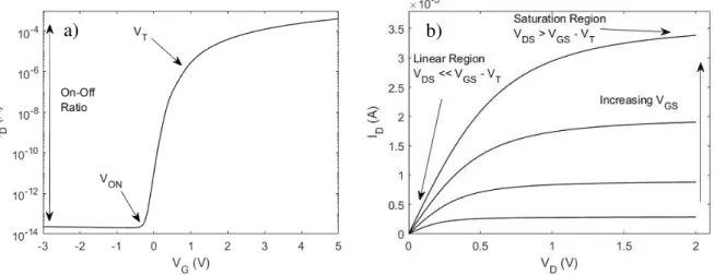
Through electrical characterization of a TFT, two common curves can be obtained: the transfer curve and the output curve. From these curves, many important TFT static characteristics can be extracted as graphically represented on Figure 1.3 and they can be summarized:
• Mobility (µ) that is related with the efficiency of carrier transport in a material, affecting directly the maximum IDS and operating frequency of devices. It can be extracted using different
methods, described below:
o Field effect mobility – obtained by the transconductance (gm) at low VDS.
𝜇𝐹𝐸 = 𝑔𝑚
𝐶𝑖𝑊𝐿 𝑉𝐷𝑆 (1.4)
with, 𝑔𝑚= 𝜕𝐼𝐷𝑆
𝜕𝑉𝐺𝑆
Parylene C as substrate, dielectric and encapsulation for flexible electronics applications 5
𝜇𝑆𝑎𝑡=
(𝜕√𝐼𝜕𝑉𝐷𝑆
𝐺𝑆 )
1
2 𝐶𝑖𝑊𝐿
2
(1.5)
• Subthreshold slope (S) indicates the necessary VGS to increase IDS by one decade, it is given by
the inverse of the maximum slope of the transfer characteristic.
𝑆 = (𝜕 log 𝐼𝜕𝑉 𝐷𝑆
𝐺𝑆 | 𝑚𝑎𝑥)
−1
(1.6)
• On/Off ratio is the ratio between the maximum of IDS and the minimum.
• Turn-on voltage (VON) is the value of VGS at which IDS starts to increase, i.e., the VGS below
which the transistor is fully turn-off.
Figure 1.3 – Typical TFT curves. a) transfer curve, b) output curve
The extraction of these parameters allows the characterization of the device performance. For the well established technology on CENIMAT based on IGZO semiconductor and sputtered oxides dielectrics, VON close to zero, On/Off ratios of near 106-107 and mobilities of 20 were achieved.
1.4
Hybrid TFTs
Flexible devices fabricated on polymeric substrates are expected to meet the emerging requests for flexible electronic applications and, this technology cannot be accomplished with silicon based electronics [31]. The conventional TFTs are inorganic based on silicon and compound semiconductors for its attractions such as high carrier mobilities, but like mentioned before the flexibility required for the flexible electronic applications cannot be obtained with silicon based technology and it has a high temperature processing [13, 32].
Organic TFTs have received a lot of attention mostly due to their low temperature processing, low-cost fabrication process and compatibility with plastics, however, they have several flaws like
Parylene C as substrate, dielectric and encapsulation for flexible electronics applications 6
environmental instability, low mobility and low on/off ratio [13]. The mentioned flaws are mostly due to the organic semiconductors, which are highly sensitive to oxygen species present in ambient air [13]. So, to reach the high carrier mobilities and the mechanical flexibility, the compound semiconductors can be combined with organic insulators. Taking advantage of good insulating properties that polymeric dielectrics have, leading to a low leakage organic gate dielectric, and the high mobility that oxide semiconductors have [11, 32].
Parylene C as substrate, dielectric and encapsulation for flexible electronics applications 7
2.
Materials and Methods
2.1
Production Techniques
To produce the devices presented in this work several fabrication techniques were used.
For the parylene deposition (substrate, dielectric and encapsulation layers), a special CVD system was used. For the TFT devices the semiconductor IGZO film was produced by sputtering in a magnetron sputtering system PVD AJA ATC 1300F with near 40 nm of thickness. The contacts with 100 to 200 nm were produced by thermal evaporation of aluminum. All the steps of the process are explained on a schematic on Appendix A.
All layers except the parylene layers were patterned using shadow masks already existed at CENIMAT, but it was necessary to develop new masks to open access to the contacts by dry etching and to produce different area MIM capacitors. The drawings of these masks can be consulted on Appendix B.
To study the parylene as dielectric, the parylene thickness was varied between 100 nm and 1.5µm and in addition it was conducted an UV-Ozone (Novascan PSD-UV) exposure study, being the time of exposure varied between 0 min and 30 min.
2.1.1
Parylene Deposition System (CVD)
The parylene C thin films are produced by chemical vapor deposition (CVD) using a Specialty Coating System Model PDS 2010 Labcoter 2. The CVD system is composed of three main chambers: a vaporization chamber, a pyrolysis chamber also known as the furnace and a polymerization chamber. A vacuum system will insure vacuum during the polymerization/deposition process and a cold trap before the vacuum pump will avoid contamination of the pump by trapping the parylene molecules, as presented on Figure 2.1.
Parylene C as substrate, dielectric and encapsulation for flexible electronics applications 8 Figure 2.1 - Parylene deposition system. From [41].
In this work, the furnace was set to 690 ºC, the evaporation chamber was cycled until a maximum temperature of 175 ºC, the pressure inside the chamber was kept at near 16 mTorr (2.1 Pa). The mass of the dimer was varied depending on the thickness desired. Silquest A-174 silane (3-methacryl-oxypropyl-trimethoxy-silane), an adhesion promoter that improves the adhesion of parylene to the materials where it will be deposited was also used for the dielectric and encapsulation layers [35]. For the substrate layer, it is not necessary the use of the adhesion promoter since the aim is to peel off the substrate.
2.2
Characterization Techniques
For every parylene deposition a piece of silicon was placed close to the sample with a part covered with Kapton tape. The thickness of the film was measured with a profilometer Ambios XP-Plus 200 Stylus.
To do the structural characterization of the films a XRD diffractometer from PANalytical, model
X’Pert Pro was made to make X-ray diffraction analysis in Bragg-Brentano geometry with Cu Kα line radiation (λ=1.5406 Å).
For the mechanical characterization a Miniature Materials Tester – Minimat was used to perform tensile tests on parylene films.
In order to get a better view of the morphology of the layers, scanning electron microscopy (SEM) was performed using an Zeiss Auriga CrossBeam system. Optical microscopy using a Leica M80 was also used in order to see if there were any flaws at the contacts and the substrate.
The electrical characterization of the MIM capacitors was performed using a semiconductor parameter analyzer (Keysight B1500A) connected to a probe station (Cascade EPS150 triax), measuring
both the capacitance−voltage, in the range of -2V to 2V, and capacitance-frequency characteristics, in the range of 0.1 Hz to 1 MHz, of the devices.
The TFTs were electrically characterized using a semiconductor parameter analyzer (Agilent 4155C) linked to a microprobe station (Cascade Microtech M150) and controlled by the software Metrics ICS. The measurements were conducted in a dark environment at room temperature. This characterization
Parylene C as substrate, dielectric and encapsulation for flexible electronics applications 9
3.
Results and Discussion
3.1
Parylene C Characterization
3.1.1
Mass-thickness calibration
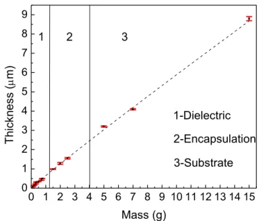
Parylene polymerizes at room temperature covering all the available surfaces on the deposition chamber. Therefore, the thickness of the film deposited on a run depends on the amount of samples/surfaces present, the pressure achieved during the deposition, the vacuum level and therefore is not a very precise variable. The control of the thickness is therefore done by controlling the amount of dimer that is inserted on the system, and thus a calibration is required. For that, during several depositions of parylene the thickness of the obtained films was always measured and a correlation between the dimer mass and the thickness can be obtained, as represented on Figure 3.1. In order to describe this relation a nonlinear regression was applied resulting in the following power function that has the better approximation to the experimental data with a R2 of 0.9964:
𝑦 = 652.20 𝑥0.96 (3.1)
In the above expression y represents the thickness of the deposited film in nanometers and x is the dimer mass in grams.
This relation can have some error, since for the same dimer mass the thickness is not exactly always the same. One factor that can influence the thickness of the deposited film is the cleanliness of the parylene deposition system, mainly the polymerization chamber.
0 1 2 3 4 5 6 7 8 9 10 11 12 13 14 15 0
1 2 3 4 5 6 7 8 9
3 2
3-Substrate 2-Encapsulation
T
hi
c
k
nes
s
(
m)
Mass (g)
1-Dielectric 1
Parylene C as substrate, dielectric and encapsulation for flexible electronics applications 10
The aim of this thesis is to use parylene C in three different layers of TFTs, each layer has a different function and therefore it needs to have different thicknesses. As represented on Figure 3.1, the dielectric layer is the thinner, for the substrate it is necessary to have sufficiently thick film to achieve good physical properties. The encapsulation layer has a thickness in between the other two layers just enough to have a good encapsulation.
3.1.2
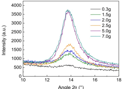
Structural Characterization
As mentioned before, parylene is a semi-crystalline polymer. In order to prove the crystallinity of parylene C it was performed an XRD analysis for different parylene thicknesses with a range of angle 2θ between 10° and 40° from this analysis it was only obtained one peak that is represented at the diffractogram at Figure 3.2. The peak is around 14° and represents the parylene C crystalline plane (0 2 0) of the monoclinic structure [36].
10 12 14 16 18
0 500 1000 1500 2000 2500 3000 3500 4000
0.3g 1.5g 2.0g 2.5g 5.0g 7.0g
Intens
ity
(a.u.)
Angle 2 (°)
Figure 3.2 - Diffractogram from XRD analysis for different parylene thicknesses
The results of the XRD analysis shows an increase of the crystallinity with the parylene thickness, what is expected since the amount of material is higher, what consequently causes an increase of the amount of crystalline material. The degree of crystallinity is one of its most important physical parameters, for semi-crystalline polymers as parylene, since it reflects the sample’s morphology and
determines various mechanical properties, such as the Young’s modulus and yield stress.
Parylene C as substrate, dielectric and encapsulation for flexible electronics applications 11
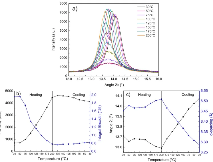
The XRD results, Figure 3.3 a), shows a peak at 13.74°, representing the parylene C crystalline plane (0 2 0). These results exhibit how the temperature influence the crystallinity. From the diffractogram on Figure 3.3 a) it can be observed the increase of the peak’s intensity and a shift of the peak for lower 2θ
angles while the temperature is raised. The decrease of 2θ represents an increase of the plane spacing and therefore indicates a dilation of the lattice. When the temperature is ramped down, the peak shifts to higher 2θ values, indicating a contraction of the lattice.
12.0 12.5 13.0 13.5 14.0 14.5 15.0 15.5 16.0 0 1000 2000 3000 4000 5000 6000 7000 8000 30°C 50°C 75°C 100°C 125°C 150°C 175°C 200°C
Angle 2 (°)
Intensi
ty
(a.u.
)
a)
30 50 75 100 125 150 175 200 175 150 125 100 75 50 30
0 1000 2000 3000 4000 5000 Temperature (°C) Intens ity (a.u.) 0.6 0.8 1.0 1.2 1.4 1.6 1.8 2.0 Cooling Integral Breadth (°2 ) Heating b)
30 50 75 100 125 150 175 200 175 150 125 100 75 50 30
13.6 13.7 13.8 13.9 14.0 14.1 c) An gl e 2 (°) Temperature (°C) 6.25 6.30 6.35 6.40 6.45 6.50 6.55 Cooling Heating d-spac ing (Å )
Figure 3.3 –In situ XRD analysis with temperature. a) Diffractograms for different temperatures. b) Dependence with
temperature of the intensity and width of the parylene peak. c) Dependence with temperature of the angle 2θ of the parylene
peak
Looking at Figure 3.3 b), it is possible to see that the intensity of the peak increases when the sample is heated, and when the temperature starts to decrease there is a little decreasing of the intensity followed by the 2θ shift. Even when the temperature decreases to the starting temperature the crystallinity remains relatively constant during the cooling. In the same figure, it is represented how the temperature influences the integral breadth (the width of a rectangle possessing the peak area and the peak intensity), confirming the conclusions about the crystallization.
Parylene C as substrate, dielectric and encapsulation for flexible electronics applications 12
cool down there is a shift of the angle to the right, what means the angle 2θ increases, so the d-spacing decreases, existing a compression on the crystalline plane (0 2 0) of approximately 0.25 Å. Although there is expansion and compression of the crystalline lattice on the plane (0 2 0) the final state is much compressed than the initial state.
3.1.3
Mechanical characterization
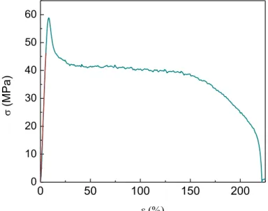
As mentioned at section 1.2, parylene mechanical properties are very important when used as substrate. To mechanically characterize parylene it was used 9 µm thick films to perform five tensile mechanical tests by applying a tensile load so the strain velocity is constant, obtaining stress/strain curves, an example is presented at Figure 3.4. From these results is possible to determine important mechanical properties such as Young’s modulus, yield strength and yield strain.
0 50 100 150 200
0 10 20 30 40 50 60
(MPa)
Figure 3.4 - Stress/strain curve of parylene
From the obtained stress/strain curve it can be observed an abruptly decrease right on the transition from the elastic region and the plastic region. After this decrease, the film starts to deform with a constant stress applied. This behavior have already been reported at [24].
From the analysis of the curve’s slope in the elastic deformation region, the Young’s modulus of the
material can be obtained. From the several tests performed, the mean Young’s modulus obtained was
0.79 GPa, being all the values between 0.45 GPa and 1.19 GPa. These values are smaller than the one reported on the datasheet of 2.8 GPa [37]. Although the value obtained is not close to the theoretical value, it is high enough for the desired applications, such as electronic skin.
Parylene C as substrate, dielectric and encapsulation for flexible electronics applications 13
words, represents the strain where there is the transition from elastic to plastic region. This value is smaller than 2.9% that was reported on the datasheet [37].
The difference on the young’s modulus might be due to assembly problems during the tests, since the film reach the yield stress for a value really close to the reported value, but the young’s modulus is
smaller than the expected, meaning that for the same stress there is more strain. The cause of the higher strain may be due to the slip of the film from the system claws and considering the small thickness of the film it is difficult to handle the films during the assembly.
Despite the results are not in full accordance with the datasheet, very similar results can be seen on [38].
3.1.4
Electrical characterization
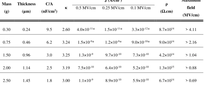
In order to study the electrical properties of parylene C samples composed of MIM capacitors with five different thicknesses were produced. The samples were produced using the shadow masks presented on Appendix B, where six capacitors with different areas were patterned (2×2 mm2, 1.5×1.5 mm2, 1×1
mm2, 0.75×0.75 mm2, 0.5×0.5 mm2 and 0.25×0.25 mm2). The samples were submitted to C-V, C-f, I-V
and breakdown measurements. From the C-V curves made at 100 kHz it was possible to determine the capacitance per unit area (C/A) and the dielectric constant (κ). To have a better understanding how the capacitance changes with the frequency, C-f curves with low frequency were made using a lock in system and a bridge system, allowing to assess the capacitance per unit area of the dielectric used in the TFT devices. The resistivity (ρ) is extracted from the I-V curves and from the breakdown measurement the breakdown field and current density (J) was obtained. A summary of these results for each thickness is presented on Table 3.1, for the 1.5×1.5 mm2 size capacitor.
Table 3.1- Electrical characterization of MIM capacitors with five different insulator thicknesses, for the capacitor size 1.5×1.5
mm2
Mass (g)
Thickness (µm)
C/A (nF/cm2) κ
J (A/cm2)
ρ (Ω.cm)
Maximum field (MV/cm)
0.5 MV/cm 0.25 MV/cm 0.1 MV/cm
0.30 0.24 9.5 2.60 4.0×10-11* 1.5×10-11* 3.3×10-12* 8.7×1014 > 4.11
0.75 0.46 6.2 3.24 1.5×10-9* 1.2×10-9* 9.0×10-10* 9.0×1014 > 2.16
1.50 0.96 3.0 3.25 1.3×10⁻⁹ 9.7×10⁻¹⁰ 7.3×10⁻¹⁰ 4.2×10¹⁴ > 1.04
2.00 1.14 2.5 3.19 7.5×10⁻¹⁰ 6.4×10⁻¹⁰ 5.2×10⁻¹⁰ 1.3×10¹⁵ > 0.88
2.50 1.45 1.8 3.00 1.1×10⁻⁹ 8.9×10⁻¹⁰ 5.9×10⁻¹⁰ 6.7×10¹⁴ > 0.69
Parylene C as substrate, dielectric and encapsulation for flexible electronics applications 14
From a quick analysis of the Table 3.1 results it can be concluded that the values of κ and ρ are close to the expected when compared to the theoretical values given by PARA TECH-Parylene Coating Industry Leader, κ=3.10 at 1 kHz and ρ=1×10¹⁵Ω.cm [39]. Concerning the dielectric strength, the
breakdown was not reached in any sample, when measured up to 100V, meaning that the parylene films produced have good dielectric strength and can withstand an electric field higher than 4.11 MV/cm.
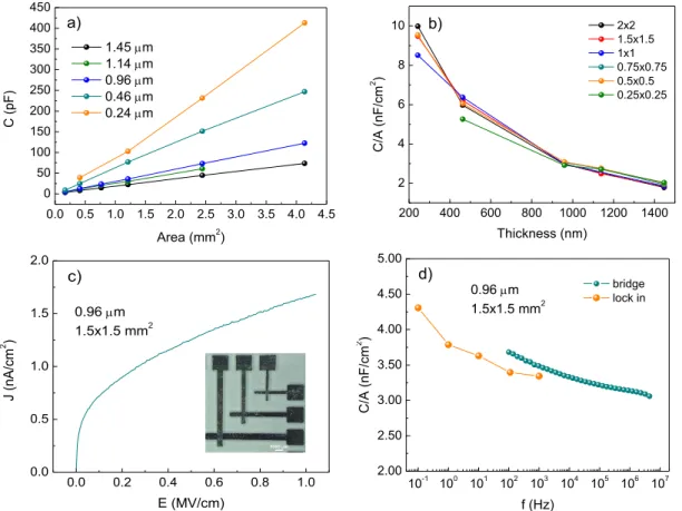
From the Figure 3.5 a) it is possible to observe the capacitance increase with the area, as it is supposed to as given by the parallel plate capacitor expression (3.1). This expression is also dependent of the dielectric thickness, so if the thickness increases the capacitance and consequently the capacitance per unit area decreases, this relation is represented at Figure 3.5 b).
𝐶 = 𝜀0𝜅𝐴𝑑 (3.1)
Where C is the capacitance, 𝜀0 represents the vacuum permittivity, κ is the parylene dielectric constant, A is the MIM capacitors area and d the parylene thickness.
0.0 0.5 1.0 1.5 2.0 2.5 3.0 3.5 4.0 4.5 0 50 100 150 200 250 300 350 400 450 C (pF )
Area (mm2) 1.45 m
1.14 m 0.96 m 0.46 m 0.24 m a)
200 400 600 800 1000 1200 1400 2 4 6 8 10 C/A (nF /c m 2 ) Thickness (nm) 2x2 1.5x1.5 1x1 0.75x0.75 0.5x0.5 0.25x0.25 b)
0.0 0.2 0.4 0.6 0.8 1.0
0.0 0.5 1.0 1.5 2.0 J (nA/c m 2 ) E (MV/cm) c)
0.96 m 1.5x1.5 mm2
10-1 100 101 102 103 104 105 106 107 2.00 2.50 3.00 3.50 4.00 4.50 5.00
0.96 m 1.5x1.5 mm2
C/A (nF /c m 2 ) f (Hz) bridge lock in d)
Figure 3.5 – Study of the electrical properties of the MIM capacitors. a) Relation between capacitance and area for different
parylene thicknesses. b) Capacitance per unit area-thickness for different sizes capacitors. c) Influence of electric field on the
current density for the 1.5×1.5 mm2 size capacitor with 0.96µm thick parylene and photograph of MIM capacitors fabricated.
d) Relation between capacitance per unit area and frequency for 1.5×1.5 mm2 size capacitor with 0.96µm thick parylene.
Parylene C as substrate, dielectric and encapsulation for flexible electronics applications 15
The Capacitance per unit area-frequency curve at Figure 3.5 d), illustrates how the capacitance per unit area of the MIM capacitor with 0.96 µm thickness changes with the frequency. Figure 3.5 d) shows that the capacitance per unit area decreases with the frequency. Additionally, it is possible to compare the κ values for different frequencies, with κ=4.10 at 1Hz and at 100kHz, for the bridge measure κ=3.48 and for the Keysight measure κ=3.25, as shown at Table 3.1. For the static characterization of TFTs, the values of capacitance per unit area at low frequency (50 Hz) are required.
From the electrical characterization, it can be concluded that parylene has good dielectric properties, leading to a low leakage currents, a good performance and expected behavior of the MIM capacitors, even on small thicknesses, since parylene can withstand high electric fields. In addition, the films are conformal and pinhole free making possible the production of big area capacitors.
3.2
Parylene as dielectric on TFTs
3.2.1
Thickness study
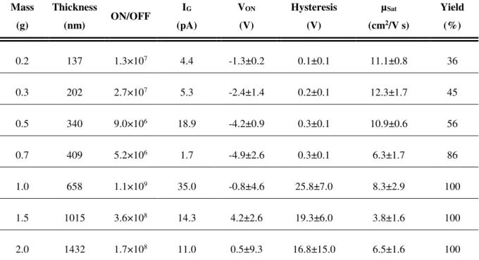
To do the calibration of the system it was needed to do several depositions with different thicknesses, and these depositions were an opportunity to study how the thickness of the dielectric can affect the behavior of the TFTs. And from that, get an idea which thickness is the best to continue the work. For the study, seven samples with different dielectric thicknesses were produced and annealed at 150°C during 1h where, each sample had two sized TFTs having the same W/L ratio (W/L=1000/100 and W/L=500/50).
To resume the main conclusions the larger TFTs are analyzed in this section but, for additional information such as the curves of the different sizes for each thickness and the parameters extracted from each condition the Appendix C can be consulted.
Parylene C as substrate, dielectric and encapsulation for flexible electronics applications 16
Table 3.2 – Electrical characterization of TFTs with different parylene dimer masses and consequently different dielectric
thicknesses.
Mass (g)
Thickness
(nm) ON/OFF
IG
(pA)
VON
(V)
Hysteresis (V)
µSat
(cm2/V s)
Yield (%)
0.2 137 1.3×10⁷ 4.4 -1.3±0.2 0.1±0.1 11.1±0.8 36
0.3 202 2.7×10⁷ 5.3 -2.4±1.4 0.2±0.1 12.3±1.7 45
0.5 340 9.0×10⁶ 18.9 -4.2±0.9 0.3±0.1 10.9±0.6 56
0.7 409 5.2×10⁶ 1.7 -4.9±2.6 0.3±0.1 6.3±1.7 86
1.0 658 1.1×10⁹ 35.0 -0.8±4.6 25.8±7.0 8.3±2.9 100
1.5 1015 3.6×10⁸ 14.3 4.2±2.6 19.3±6.0 3.8±1.6 100
2.0 1432 1.7×10⁸ 11.0 0.5±9.3 16.8±15.0 6.5±1.6 100
The results from Table 3.2, shows that the variation of the thickness causes changes in the TFTs parameters. For start, the most noticeable change is the rise of the hysteresis value with the increase of the thickness, not only the hysteresis value increases but also the standard deviation, this effect is easily observed at Figure 3.6. Other parameter that is influenced by the thickness is the VON, becoming more
negative for higher thicknesses, in this case the standard deviation also increases with the thickness. These results along with the decreasing of the mobility for higher thicknesses, shows that as dielectric thickness increases the performance of the device gets worse, once the ideal TFTs should have a hysteresis, VON value and VT value near zero, and a high mobility. The mobility decrease is expected,
because for lower thicknesses the gate dielectric capacitance is higher, meaning an increase of the carriers close to the dielectric and semiconductor interface, causing a bigger field effect what leads to an increase of the mobility and the need of more negative tensions to turn off the transistor.
For lower thicknesses, higher gate currents (IG) were expected, but the results show that for every
thickness the IG is low, in the order of the pA. This proves that even as a thin dielectric, parylene is a
Parylene C as substrate, dielectric and encapsulation for flexible electronics applications 17
-3 -2 -1 0 1 2 3
10-14 10-13 10-12 10-11 10-10 10-9 10-8 10-7 10-6 10-5 10-4 IDS (A)
VGS (V)
VDS= 6V m = 0.2g
a)
-6 -4 -2 0 2
10-14 10-13 10-12 10-11 10-10 10-9 10-8 10-7 10-6 10-5 10-4 IDS (A)
VGS (V)
VDS= 6V m = 0.5g
b)
-30 -20 -10 0 10 20 30
10-14 10-13 10-12 10-11 10-10 10-9 10-8 10-7 10-6 10-5 10-4 IDS (A)
VGS (V)
VDS= 10V m = 1.0g
c)
-20 -10 0 10 20 30
10-14 10-13 10-12 10-11 10-10 10-9 10-8 10-7 10-6 10-5 10-4 IDS (A)
VGS (V)
VDS= 10V m = 1.5g
d)
Figure 3.6 – Transfer curves of the TFTs using different dielectric thicknesses; a) corresponding to 0.2g of dimer. b)
corresponding to 0.5g of dimer. c) corresponding to 1.0g of dimer. d) corresponding to 1.5g of dimer
Additional information can also be extracted from Figure 3.6, such as the direction of the hysteresis. In the TFTs with thinner dielectric the hysteresis has a clockwise direction, in contrast for TFTs of 1.0g or more the hysteresis has an anticlockwise direction, which may indicate ionic drift.
To obtain the curves of 1.0g, 1.5g and 2.0g, it was necessary to apply a higher range of VGS, even
though the VON value is positive or near zero.
From the comparison between the two sizes of TFTs for the same thickness, there is no big differences on the results. Conclusions can be taken only on the hysteresis value that is higher for the smaller TFTs, this can be confirmed at Appendix C.
Parylene C as substrate, dielectric and encapsulation for flexible electronics applications 18
0 1 2 3 4 5 6 7
0 5 10 15 20 25 30 35 40 IDS ( A)
VDS (V)
a)
VGS= -1V to 7V
-2 0 2 4
10-14 10-13 10-12 10-11 10-10 10-9 10-8 10-7 10-6 10-5 10-4 I DS (A)
VGS (V)
V
DS=7V
m = 0.3g
b)
Figure 3.7- Electrical characterization of the TFTs with a dielectric thickness corresponding to 0.3g dimer mass. a) Output curve. b) Transfer curve.
From the output curve it can be easily concluded from which values the saturation region begins and, with that choose the gate tension used to extract the transfer curve on the saturation region.
The results from the TFT with a dielectric thickness corresponding to 0.3g dimer mass are presented in Figure 3.7 and shows a good behavior of the TFT achieving a mobility of 12 cm2.V-1s-1 a hysteresis
of 0.2 V and an ON/OFF ratio of 3×10⁷. However, the yield of working devices is 45 %., meaning that
more than half of the measured devices (the number of devices measured can be consulted at Appendix C) had high leakage currents making it impossible to obtain the TFT curves. This may be due to a poor adhesion of parylene with aluminum. Previous results from MIS structures with and without adhesion promotor showed that if the adhesion is bad, the field created can damage the parylene layer and increase leakage [6].
3.2.2
UV-Ozone surface treatment
To improve the adhesion between the aluminum of the gate electrode and parylene, the gate contacts were exposed to a UV-ozone atmosphere before the deposition of the parylene. The aim of this exposure was to oxidize or enhance the aluminum surface [40–42]. This AlOx layer will increase the creation of
bonds with the adhesion promoter (Silquest A-174 silane), and consequently improve the adhesion between the contacts and the dielectric layer [41]. A better adhesion can represent an improvement of the samples yield and a lower dispersion of the results for the same sample.
Parylene C as substrate, dielectric and encapsulation for flexible electronics applications 19
-4 -2 0 2 4 6
10-14 10-13 10-12 10-11 10-10 10-9 10-8 10-7 10-6 10-5 10-4 IDS (A)
VGS (V) t = 0 min
a)
-4 -2 0 2 4 6
10-14 10-13 10-12 10-11 10-10 10-9 10-8 10-7 10-6 10-5 10-4
t = 5 min
IDS
(A)
VGS (V)
b)
-4 -2 0 2 4 6
10-14 10-13 10-12 10-11 10-10 10-9 10-8 10-7 10-6 10-5 10-4 I DS (A)
VGS (V)
t = 15 min c)
-12 -10 -8 -6 -4 -2 0 2 4 6 10-14 10-13 10-12 10-11 10-10 10-9 10-8 10-7 10-6 10-5 10-4 I DS (A)
VGS (V) t = 30 min
d)
Figure 3.8- Transfer curves of TFTs with VDS=7V, from UV-ozone tests performed before parylene deposition with different
exposure times: a) no exposure; b) 5 min; c) 15 min and d) 30 min.
Observing Figure 3.8 an increment of the dispersion for the same sample can be seen. This refutes the idea that the exposure to UV-ozone improves the TFTs performance. In addition, the results from Table 3.3 proves that exposure worsens the TFTs performance.
Table 3.3 – Electrical characterization of TFTs with different UV-ozone exposure times.
Time (min)
VT
(V) ON/OFF ISat (µA) IG (pA) VON (V) S (V/dec) Hysteresis (V) µSat
(cm2/V s)
Yield (%)
0 4.2±0.2 9.3×10⁷ 3.9 4.4 0.0±0.6 0.16±0.06 1.2±0.2 4.0±1.4 89
5 3.5±0.2 1.5×10⁸ 11.1 3.3 -1.2±0.5 0.23±0.11 0.9±0.2 7.4±0.7 100
15 3.0±0.2 1.4×10⁸ 14.6 3.2 -2.3±0.8 0.27±0.05 0.8±0.2 6.8±1.1 100
Parylene C as substrate, dielectric and encapsulation for flexible electronics applications 20
On Table 3.3, can be observed that the VON value becomes more negative with exposure time as well
as standard deviation. In contrast, there is an improvement on the hysteresis, that means the decreasing of the hysteresis value. And the mobility of the samples exposed increases comparing to the not exposed sample, being the mobility values similar among the exposed samples. This behavior might be due to the formation of AlOx during the exposure, that will increase the capacitance of the dielectric since AlOx
has a larger κ than the parylene. As mentioned before the capacitance increase will influence the mobility and also the VON value.
Although the hysteresis decreases with exposure time, when it comes to the other parameters the difference is not substantial. Making not exposing possibly the best option, once the VON value has more
impact on the device performance than the hysteresis. The yield increase with exposure time indicating that adhesion plays an important role for the TFTs operation.
3.2.3
Top Gate vs Bottom Gate structures
As mentioned before, the parylene deposition is by a special CVD process. This process is not aggressive for the material where the parylene will be deposited because it is not a physical process. This allows the production of TFTs with the configuration staggered top gate since the semiconductor layer is not damaged by the parylene deposition process as it would be for common sputtered dielectrics, overcoming the main difficulty of producing staggered top gate TFTs that is to have a dielectric deposition process compatible with the semiconductor layer. The top gate configuration also has the advantage to encapsulate the active layer with the dielectric layer.
For this study two configurations, staggered bottom gate and staggered top gate, were made at the same time, where only the semiconductor layer deposition was not the same for both configurations. The TFTs produced have a dielectric thickness of approximately 250 nm and were accidentally annealed at 195°C during 1h.
Parylene C as substrate, dielectric and encapsulation for flexible electronics applications 21 -10 -8 -6 -4 -2 0 2 4 6
10-13 10-12 10-11 10-10 10-9 10-8 10-7 10-6 10-5 10-4 10-3 10-2 IDS (A)
VGS (V) VDS=7V
a)
-10 -8 -6 -4 -2 0 2 4 6 10-13 10-12 10-11 10-10 10-9 10-8 10-7 10-6 10-5 10-4 10-3 10-2 IDS (A)
VGS (V) VDS=7V
b)
-2 0 2 4 6
10-13 10-12 10-11 10-10 10-9 10-8 10-7 10-6 10-5 10-4 10-3 10-2
VDS=7V
ID S
(A)
VGS (V)
c)
After 1 month
-10 -8 -6 -4 -2 0 2 4 6 10-13 10-12 10-11 10-10 10-9 10-8 10-7 10-6 10-5 10-4 10-3 10-2
After 1 month
IDS
(A)
VGS (V) VDS=7V
d)
Figure 3.9 - Transfer curves of bottom gate configuration and top gate configuration. a) Bottom gate configuration
characterized after the production, representation of all layers of the device from [43], b) Top gate configuration characterized
after the production, representation of all layers of the device from [43], c) Bottom gate configuration characterized after one
month, d) Top gate configuration characterized after one month.
The TFTs were measured after the production and approximately one month later, as presented at Figure 3.9, the results show that after a month the bottom gate TFTs have a typical transfer curve, with lower drain current and channel modulation, and the top gate TFTs remain too conductive. These results prove that the parylene dielectric layer really encapsulates the semiconductor on the top gate configuration, since there was not any alteration of the top gate TFT behavior after an exposure to atmospheric conditions.
At Table 3.4 are the parameters extracted from the curves of the bottom gate TFTs.
Table 3.4 - Electrical characterization of the bottom gate sample one month after the production
VT
(V) ON/OFF ISat (µA) IG (pA) VON (V) S (V/dec) Hysteresis (V) µSat
(cm2/V s)
Yield (%)
Parylene C as substrate, dielectric and encapsulation for flexible electronics applications 22
After one month, the bottom gate TFTs present good parameters, such as good ON/OFF ratio, low gate current, VON value near zero, low hysteresis and high mobility.
Although the bottom gate TFTs behave properly and have good parameters, the yield was very low (33% having 12 devices measured). One reason that might justify the low yield is the high annealing temperature that caused bubbles on the TFTs contacts and channel, Figure 3.10.
Figure 3.10 – Bottom gate samples after the high temperature annealing, formation of the bubbles on the contacts and
channel.
The bubbles formed on the sample were not present on the substrate and, it could only be observed on the TFTs. Additionally, the TFTs are also with scratches what might be due to different thermal expansion coefficients. The bubble formation could lead to short circuits in the TFTs which caused a high gate current.
3.3
Parylene as encapsulation layer
From the top gate TFTs it was proven that the parylene dielectric layer encapsulates the semiconductor. Since the results shows that parylene have low permeability able to encapsulate the active layer, this material can be used as encapsulation layer on bottom gate TFTs. Furthermore, it has been reported that parylene as encapsulation layer increases the electrical stability since parylene effectively block the diffusion of atmospheric species to IGZO, it also neutralizes defects at the channel surface [44].
To study how the parylene encapsulation layer affects the bottom gate TFTs performance, a sample of bottom gate TFTs were produced and characterized and then it was encapsulated with an additional layer of parylene and characterized again.
The TFTs produced have a dielectric thickness of approximately 450 nm and were annealed at 150°C during 1h. The thickness was higher than the optimal defined at section 3.2.1, due to problems on the system cleanliness. For the encapsulation a parylene film with approximately 1.5µm was used.
Parylene C as substrate, dielectric and encapsulation for flexible electronics applications 23
-6 -4 -2 0 2 4
10-14 10-13 10-12 10-11 10-10 10-9 10-8 10-7 10-6 10-5 10-4 IDS (A)
VGS (V)
VDS=7V
a)
-2 0 2 4
10-14 10-13 10-12 10-11 10-10 10-9 10-8 10-7 10-6 10-5 10-4 IDS (A)
VGS (V)
VDS=7V
b)
Figure 3.11 – Electrical characterization of TFTs, a) without encapsulation layers, b) after the deposition of parylene
encapsulation layer
From Figure 3.11 it is possible to see a shift of the VON to more positive values, what represents an
improvement of the TFT operation. All the changes of the TFT parameters are presented at Table 3.5.
Table 3.5 – Parameters extracted from the electrical characterization of the TFTs before and after the encapsulation
VT
(V) ON/OFF ISat (µA) IG (pA) VON (V) S (V/dec) Hysteresis (V) µSat
(cm2/V s)
Before 2.1±0.6 2.4×10⁶ 5.7 5.4 -3.0±1.6 0.42±0.04 0.5±0.1 8.2±1.3
After 3.0±0.1 1.2×10⁶ 1.8 3.9 0.1±0.2 0.32±0.09 0.6±0.3 6.0±0.7
The TFTs encapsulation causes several changes on the TFT parameter, as can be seen on Table 3.5, the VON value becomes more near zero and has less dispersion, the S decreases and the leakage current
also decreases what suggest an improvement of the TFT performance. But not all changes are for the best, there is a slight decrease of the saturation current and the mobility decreases as well. Further tests and the production of new devices will allow to clarify this phenomenon or to conclude if these results was due to sample handling instead.
From these results, despite not all the parameters improve it can be concluded that after the encapsulation the TFTs have a better performance since the improvements are more significant than the worsening.
3.4
Parylene as substrate
Parylene C as substrate, dielectric and encapsulation for flexible electronics applications 24
parylene C substrate. All the layers of the TFTs were produced in the same depositions. Both samples were annealed at 150°C during 1h.
The Figure 3.12 shows the difference of a device transfer curve of each sample.
-4 -2 0 2 4 6
10-14 10-13 10-12 10-11 10-10 10-9 10-8 10-7 10-6 10-5 10-4 IDS (A)
VG (V)
a)
-4 -2 0 2 4
10-14 10-13 10-12 10-11 10-10 10-9 10-8 10-7 10-6 10-5 10-4 IDS (A)
VGS (V)
b)
Figure 3.12 – Transfer curves of a TFT with a VDS=7V. a) on corning glass substrate, b) on parylene substrate.
Observing Figure 3.12 there is no big differences between the two samples, the more evident difference is the ON/OFF ratio, being smaller for the sample with the parylene substrate.
Table 3.6 - Parameters extracted from the electrical characterization of the TFTs on corning glass and on parylene C substrate
VT
(V) ON/OFF ISat (µA) IG (pA) VON (V) S (V/dec) Hysteresis (V) µSat
(cm2/V s)
Corning
glass 2.6±0.3 2.8×10
7 13.6 2.6 -3.7±1.0 0.22±0.24 1.1±0.2 7.9±0.7
Parylene C 2.6±0.8 2.6×10⁶ 4.9 4.5 -2.0±1.1 0.35±0.14 0.6±0.3 7.6±0.5
From Table 3.6 it is easier to compare the results, and there are actually more differences in addition to the ON/OFF ratio. The saturation current is lower on the TFTs with parylene substrate what directly influences the ON/OFF ratio. The VON is less negative and the hysteresis is lower for the sample with
the parylene substrate what show some advantages of using the parylene as a substrate. The S is higher than the one of the corning glass sample but the difference is not that significant.
Parylene C as substrate, dielectric and encapsulation for flexible electronics applications 25
When using parylene as substrate it is very important to use relatively low annealing temperature. From a sample annealed at 195°C, Figure 3.13, it is possible to prove that high annealing temperature can damage the sample.
Figure 3.13- Substrate cracks due to heating. a) Optical microscope image of the edge of the substrate. b) SEM image of the parylene substrate among the TFTs
At Figure 3.13 it can be seen the substrate of a sample after 1h under 195°C, the substrate shows some cracks, what might be due to the difference of the thermal expansion coefficients of the parylene and the carrier. As seen at section 3.1.2 the parylene expand and compress with temperature, and the final state is more compressed than the initial state and, this behavior can justify why the parylene cracks when annealed at 195ºC.
These substrate cracks might affect the TFT performance and the most critical consequence is the impossibility of using as a flexible substrate, since it is not physically stable without the carrier.
3.5
Peel off from the carriers
The final step to achieve a fully conformal and flexible device is to do the substrate peel off. In order to obtain a thin film detached from the carrier several tests were conducted. For this tests parylene films were deposited on glass without using the adhesion promoter.
The first attempt to do the peel off was simply using the tweezer and try to pull the film, this attempt was not successful, since the tweezer damage the film due to the very low thickness. Moreover, the film breaks during the pull out because the force applied at the film is not uniform.
To try to solve the problems caused by the tweezer, another method was tried. This method consists at making a window with Kapton tape around the film and then pull the tape, it was adapted from [38], as can be seen at Figure 3.14.
Parylene C as substrate, dielectric and encapsulation for flexible electronics applications 26
Figure 3.14 – Photograph of the peel-off method with the Kapton tape.
With this method it was possible to peel-off a parylene film as thin as 1µm thick, as shown in the Figure 3.14. When the sample is heated it is not possible to peel-off with this method since the film gets stuck to the glass when the tape is pulled, only the parylene in contact whit the tape is removed and the film inside of the window remained on the glass.
The last approach was an adaptation of [45], and started by depositing a film of polyvinyl alcohol (PVA) on the glass carrier before the parylene deposition. After the parylene deposition, to peel-off the film, is necessary to immerse the sample in water so the PVA can dissolve and the parylene film start to detach from the glass.
Figure 3.15- Peel-off of a sample with a PVA film under the parylene C, different phases of the peel-off.
In fact, the parylene film did not detached from the glass just by putting the sample in water. It was needed to heat the water to help the dissolution of the PVA and to use the tweezer to pull the film while it was on the water, as seen at Figure 3.15. This method is less destructive to the film than the method using only the tweezer and the method with the tape and it can also peel thin films, such as the one in Figure 3.15, with 3µm thick.
Parylene C as substrate, dielectric and encapsulation for flexible electronics applications 27
Considering the TFTs produced at section 3.4, where a parylene film with 1µm thick is already used as substrate without the PVA layer below, the peel-off of these films was made using the method with the tape.
Figure 3.16 – Parylene film with 1 µm thick as substrate with TFTs.
Since the sample was annealed so the TFTs were characterized, the film did not peel as well as at Figure 3.14, and it break during the peel-off. From this attempt a small sample was obtained, as it can be seen at Figure 3.16 the sample is really conformal and highly flexible. The parylene substrate have a good adhesion to the skin and it is ergonomic what makes a good candidate to skin electronics.
3.6
Parylene as dielectric, encapsulation and substrate
To fully complete the objectives, devices with parylene as substrate, dielectric layer and encapsulation layer were produced. Initially it was deposited a PVA layer before the start of the TFTs production in order to help the peel off the devices after all layers are deposited. It can be observed a schematic of all layers on Figure 3.17, in addition it can be seen the thicknesses of each layer of parylene C.
Figure 3.17 - TFT’s schematic with the thickness of all parylene layers defined.
These devices were characterized before and after the off by the PVA method. After the peel-off the film shrinks and to be able to electrically characterize it was necessary to glue the sample with Kapton tape to a glass in order to flatten the sample.
![Figure 1.1-Three most common parylene types. Adapted from [17]](https://thumb-eu.123doks.com/thumbv2/123dok_br/16698378.743911/26.892.140.767.380.546/figure-common-parylene-types-adapted.webp)
![Figure 1.2 -Different TFT structures. From [28].](https://thumb-eu.123doks.com/thumbv2/123dok_br/16698378.743911/27.892.213.720.735.1062/figure-different-tft-structures-from.webp)