Novembro, 2014
Vasco Alexandre Violante Rodrigues
Licenciatura em Ciências de Engenharia em Micro e Nanotecnologias
Digital Microfluidic devices: the role of the dielectric layer
Dissertação para obtenção do Grau de Mestre em Engenharia de Micro e Nanotecnologias
Orientador: Professor Doutor Rui Igreja, Dep. Ciência dos Materiais, FCT-UNL Co-orientador: Professor Doutor Hugo Águas, Dep. Ciência dos Materiais, FCT-UNL
Júri:
Presidente: Prof. Doutor Rodrigo Ferrão de Paiva Martins Arguente: Doutora Rita Maria Mourão Salazar Branquinho
D
IGITAL
M
ICROFLUIDICS
:
T
HE ROLE OF THE
DIELECTRIC LAYER
© Vasco Alexandre Violante Rodrigues
Faculdade de Ciências e Tecnologia
Universidade Nova de Lisboa
A
GRADECIMENTOS
É com enorme satisfação que vejo cumprida mais uma etapa da minha vida, tendo sido esta porventura uma das mais exigentes até ao momento. A conclusão deste trabalho encerra em si um capítulo que começou por ser caracterizado por grande incerteza, tendo eu pertencido ao reduzido grupo de pessoas que ingressou pela primeira vez no Mestrado Integrado em Engenharia de Micro e Nanotecnologias, e é com alegria que pertenço ao grupo ainda mais restrito de pessoas que o conclui agora, cinco anos volvidos.
No desenvolvimento deste trabalho, com um papel importantíssimo para que este pudesse ser realizado com qualidade e rigor, contei com o apoio do meu orientador, Professor Doutor Rui Igreja, ao qual agradeço verdadeiramente. Sem o seu apoio e metodologias de trabalho, não teria sido possível cumprir algumas das principais metas propostas, e reconheço hoje que deveria ter tido em maior consideração todos os seus alertas. Agradeço a oportunidade que me deu de desenvolver este trabalho com alguma liberdade e por ter sido um orientador na verdadeira acepção da palavra. Agradeço também ao meu co-orientador, Professor Doutor Hugo Águas, por todas as contribuições para o meu trabalho, e por ter manifestado sempre disponibilidade para me auxiliar em qualquer necessidade ou dúvida. Estendo os agradecimentos ao Professor Doutor Ricardo Franco e à sua equipa, pelo seu prezado auxílio nos testes biológicos para concretização da prova de conceito e pelas sugestões sempre úteis que proporcionou ao longo de todo o trabalho, que acompanhou desde o início. Quero ainda agradecer a todas as pessoas do Centro de Investigação de Excelência CENIMAT que me auxiliaram ao longo do trabalho, em especial à Doutora Joana Pinto por todo o apoio nas deposições e à Investigadora Daniela Gomes pela ajuda na obtenção de imagens de microscopia electrónica de varrimento.
Às pessoas com as quais partilhei o meu local de trabalho nos últimos meses, agradeço especialmente à Inês Cunha pela infinidade de vezes que me emprestou o cartão para acesso à câmara limpa, e ao João Resende, que apesar de chegar mais tarde, rapidamente se juntou ao grupo.
Aos meus inicialmente apenas colegas com que entrei no curso e hoje verdadeiros amigos com os quais passei alguns dos melhores momentos da minha vida, não há palavras para agradecer a todos vós: Ana Correia, Paul Grey, Miguel “Rambo” Soares, Daniel “Caril” Matos e Gonçalo Rodrigues. Sei que esta amizade se irá prolongar muito para além da faculdade, independente do que a vida trouxer a cada um de nós.
À minha família não tenho como agradecer o suficiente. O apoio dos meus pais e irmã em todos os momentos, e todos os seus esforços para que pudesse ter uma educação que me permitisse alcançar os meus objectivos, são algo que nunca poderei retribuir. Se em algum momento pensarem se haveria algo mais que pudessem ter feito, acreditem que já fizeram demasiado e nada mais vos poderia ter pedido. A todas as pessoas que aqui não referi mas que me ajudaram a crescer ao longo deste percurso de uma ou de outra forma, agradeço profundamente, mesmo que nunca cheguem a ler estas linhas. A todos o meu sincero obrigado!
A
BSTRACT
Digital microfluidics (DMF) is a field which has emerged in the last decade as a re-liable and versatile tool for sensing applications based on liquid reactions. DMF allows the discrete displacement of droplets, over an array of electrodes, by the application of voltage, and also the dispensing from a reservoir, mixing, merging and splitting fluidic operations. The main drawback of these devices is due to the need of high driving volt-ages for droplet operations. In this work, alternative dielectric layers combinations were studied aiming the reduction of these driving voltages. DMF chips were designed, pro-duced and optimized according to the theory of electrowetting-on-dielectric, adopting different combinations of parylene-C and tantalum pentoxide (Ta2O5) as dielectric
ma-terials, and Teflon as hydrophobic layer.
With both devices’ configurations, i.e., Parylene as single dielectric, and multilayer
chips combining Parylene and Ta2O5, it was possible to perform all the fluidic
opera-tions in the microliter down to hundreds of nanoliters range.
Multilayer chips presented significant reduction on driving voltages for droplet op-erations in silicone oil filler medium: from 70 V (parylene only) down to 30 V (parylene/Ta2O5) for dispensing; and from 50 V (parylene only) down to 15 V
(parylene/Ta2O5) for movement. Peroxidase colorimetric reactions were successfully
performed as proof-of-concept, using multilayer configuration devices.
Keywords: Digital microfluidics; dielectrics; electrowetting-on-dielectric; parylene-C; tantalum pentoxide.
R
ESUMO
A microfluídica digital é um campo que emergiu na última década como uma ferramenta fiável e versátil para utilização no ramo das aplicações em sensores baseados em reacções no estado líquido. A microfluídica digital permite a movimentação de gotas sobre uma matriz de eléctrodos, por aplicação de tensão, e ainda as operações fluídicas de extracção a partir de reservatórios, mistura, fusão e separação. O principal inconveniente destes dispositivos deve-se à necessidade de aplicar tensões elevadas para executar operações fluídicas. Neste trabalho, foram estudadas combinações de camadas dieléctricas alternativas com vista a reduzir as tensões de operação. Os dispositivos foram projectados, produzidos e optimizados de acordo com os princípios deredução do ângulo de contacto com aplicação de tensão em dieléctricos, utilizando diferentes combinações de parileno-C e pentóxido de tântalo (Ta2O5) como materiais dieléctricos,
e Teflon como camada hidrofóbica.
Com ambas as configurações de dispositivo, i.e., tendo o Parileno como único
dieléctrico e multicamadas combinando Parileno e Ta2O5, foi possível executar todas as
operações fluídicas na escala dos microlitros até às centenas de nanolitros.
Os dispositivos multicamada possibilitaram a redução significativa das tensões de actuação para as operações fluídicas realizadas em meio de óleo de silicone: de 70 V (apenas parileno) para 30 V (parileno/Ta2O5) na operação de extracção de gotas de um
reservatório; e de 50 V (apenas parileno) para 15 V (parileno/Ta2O5) para
movimentação de gotas.
Foram ainda realizadas com sucesso reacções colorimétricas de peroxidase utilizando uma configuração multicamada como prova de conceito.
Palavras-chave: Microfluídica digital; dieléctricos; electrowetting-on-dielectric;
parileno-C; pentóxido de tântalo.
L
IST OF ACRONYMS
ABTS – 2,2'-azino-bis(3-ethylbenzthiazoline-6-sulphonic acid ALD – Atomic Layer Deposition
BST – Barium Strontium Titanate BZN – Barium Zinc Niobate CA – Contact Angle
CEMOP/UNINOVA – Centro de Excelência de Optoelectrónica e Microelectrónica de Processos
CENIMAT/I3N – Centro de Investigação de Materiais/ Instituto de Nanoestruturas, Nanomodelação e Nanofabricação
CL – Load Capacitance CT – Tune Capacitance DEP – Dielectrophoresis DI – Deionized
DMF – Digital microfluidics DNA – Deoxyribonucleic Acid EW – Electrowetting
EWOD – Electrowetting on dielectric FIB – Focused Ion Beam
ITO – Indium Tin Oxide
LPCVD – Low-Pressure Chemical Vapor Deposition
MOCVD – Metal Organic Chemical Vapor Phase Deposition PBS – Phosphate buffered saline
PTFE – Polytetrafluoroethylene RPM – Revolutions per minute
SEM – Scanning Electron Microscope
L
IST OF SYMBOLS
t – Thickness of the dielectric V – Voltage
VT – Threshold voltage (V)
wt/wt – Mass fraction (weight/weight) XC – Capacitive reactance
γ – Interfacial energy, surface tension
γLG – Liquid–vapor interfacial energy
γSG – Solid–vapor interfacial energy
γSL – Solid–liquid interfacial energy
δ – Loss angle
θ0 – Non-actuated or initial angle
θC – Equilibrium contact angle
θV – Actuated angle
σ1 – Conductivity of the liquid
ωC – Critical frequency
𝜺𝜺0 – Permittivity in vacuum (8.854x10⁻¹² Fm-1)
𝜺𝜺1 – Dielectric constant of the liquid
𝜺𝜺r – Relative permittivity, dielectric constant
I
NDEX
AGRADECIMENTOS ... I
ABSTRACT ... III
RESUMO ...V
LIST OF ACRONYMS ... VII
LIST OF SYMBOLS ... IX
INDEX ... XI
LIST OF FIGURES ... XIII
LIST OF TABLES ... XVII
MOTIVATION ... XIX
1. INTRODUCTION ... 1
1.1 ELECTROWETTING-ON-DIELECTRIC (EWOD) ... 1
1.2 DIGITAL MICROFLUIDICS ... 1
1.3 THE ROLE OF THE DIELECTRIC LAYER ... 3
2. MATERIALS AND METHODS ... 7
2.1 PROPERTIES OF THE COMPOSING LAYERS ... 7
2.2 DEVICE FABRICATION ... 8
3. RESULTS AND DISCUSSION ... 11
3.1 ELECTROWETTING-ON-DIELECTRIC AND DIELECTRIC BREAKDOWN ... 11
3.1.1 Theoretical EWOD for parylene-C only and parylene/Ta2O5 multilayer devices ...12
3.1.2 Dielectric breakdown voltage ...12
3.1.3 EWOD experimental data vs. theoretical curves ...13
3.1.4 Frequency effect ...15
3.2 DIELECTRIC TESTS WITH PARYLENE-C AND TA2O5... 16
3.2.1 Parylene-C dielectric tests ...17
3.2.2 Tantalum pentoxide dielectric tests ...19
3.3 DEVICE STRUCTURE AND OPERATIONAL CONDITIONS ... 21
3.3.1 Structural analysis ...21
3.3.2 Further device specifications ...23
3.3.2.1 Shape, size and spacing of electrodes ... 24
3.3.2.2 Filler medium ... 25
3.3.2.3 Channel gap ... 26
3.4 FLUIDIC OPERATIONS ... 27
3.4.1 The role of the dielectric layer ...28
3.5 PROOF-OF-CONCEPT ... 30
4. CONCLUSIONS AND FUTURE PERSPECTIVES ... 31
4.1 CONCLUSIONS ... 31
4.2 FUTURE IMPROVEMENTS AND PERSPECTIVES ... 32
5. BIBLIOGRAPHY ... 33
6. APPENDIX ... I APPENDIX A ... i
APPENDIX B ... ii
APPENDIX C ... iii
APPENDIX D ... iv
APPENDIX E ... v
APPENDIX F ... vi
APPENDIX G ... vii
L
IST OF
F
IGURES
Fig. 1.1 – a) Illustration of the triphase contact line; b) Water drop over a hydrophobic surface. Top: without applied voltage (high contact angle). Bottom: with applied voltage (decrease in the contact angle value).3 ... 1 Fig. 1.2 – DMF device, where the array of electrodes is presented. Fluidic operations
also observable. Adapted from 5. ... 2 Fig. 2.1 – Patterning of the electrodes: A – Square electrodes with 30 μm gap between
electrodes; B - Square electrodes with 50 μm gap between electrodes; C -
Interdigital electrodes with 30 μm gap between electrodes; D - Interdigital
electrodes with 50 μm gap between electrodes... 8 Fig. 3.1 – Contact angle measurements in a structure. The measurements were
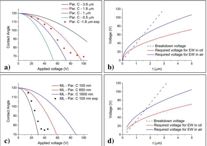
performed by introducing a needle in a 5 μL droplet of DI water with a resistivity of 15 MΩ.cm: a) high initial contact angle without voltage application, ≈118.8º; b) contact angle after applying 70 Vdc on the droplet, obtaining a final contact angle of approximately 78.7º. ... 11 Fig. 3.2 – a) Theoretical EWOD effect for different thicknesses of parylene-C and a
hydrophobic coating of 50 nm Teflon AF 1600, and experimental plot for a 1.8 μm
layer in air medium; b) Dielectric breakdown of parylene-C with Teflon AF in silicone oil and air as filler mediums; c) Theoretical EWOD effect for different combinations of Tantalum pentoxide and parylene-C coated with 50 nm of Teflon AF 1600, and experimental plot for 200 nm Ta2O5 and 100 nm of parylene-C in air
medium; d) Dielectric breakdown for different combinations of Tantalum
pentoxide and parylene-C, in silicone oil and air as filler mediums. ... 14 Fig. 3.3 – Effect of applied frequency in EW, considering a fixed value of voltage
(sinusoidal wave with 50 V of amplitude), for a 2 μL DI water with resistivity of
ca.12 MΩ.cm. The effects of volume loss and contact angle hysteresis are not to
be disregarded. These tests were performed on a layer of Parylene C without any hydrophobic coating, hence the lower initial contact angle (ca. 93-95o) comparing
to the ones verified when this type of coatings are present (ca. 120o). ... 16
Fig. 3.4 – Developed structures for the dielectric tests: a) Matrix structure for the dielectric test of Ta2O5, responsible for the distinguishable brown tone; b) Cross
structure for the dielectric test of parylene-C. ... 17 Fig. 3.5 – a) Capacitance measurements of a 550-600 nm Parylene-C layer for a range
of 100 Hz to 100 kHz; b) Loss tangent, or dielectric loss, experimental plot obtained for the measurements on the Parylene-C layer for a range of 100 Hz to 100 kHz. ... 18 Fig. 3.6 – a) Capacitance measurements of a 250 nm Ta2O5 layer for a range of 100 Hz
to 100 kHz; b) Loss tangent, or dielectric loss, experimental plot obtained on the 250 nm Ta2O5 layer for a range of 100 Hz to 100 kHz. ... 20
Fig. 3.7 – Device’s bottom plate architecture: a) Parylene-C as single dielectric covered with Teflon (not to scale); b) Multilayer dielectric structure, with Ta2O5 covering
the electrodes, followed by Parylene-C and Teflon (not to scale). ... 21 Fig. 3.8 – Device’s layered structure images acquired with SEM, after milling a select
area on a reservoir electrode recurring to FIB: a) different composing layers of the device, excepting the Teflon layer, which is harder to observe due to its
dimensions (ca. 50 nm, as previously mentioned); b) detail to show the thicknesses
of the deposited layers on glass: chromium – ≈390 nm; Ta2O5 – ≈260 nm and
Parylene-C – ≈715 nm. ... 22 Fig. 3.9 – Complete device and test platform. This platform allows for the test of
devices with up to 32 electrodes, as it is observable by the number of addressing voltage pins. The top-plate electrode is connected to ground voltage by the represented red cable. The Kapton tape spacers between bottom and top-plate are also visible. ... 24 Fig. 3.10 – Interdigital shape of electrodes and detail to exhibit the areas that facilitate
the droplet movement. ... 24 Fig. 3.11 – Fluidic operations performed with the produced devices. The devices were
composed by a 3.6 μm parylene-C dielectric layer, covered by 50 nm of Teflon, the
channel gap used was 100 μm and the electrodes were 30 μm spaced. The
operations were performed using silicone oil as filler medium. The used solutions had the concentration of 3 M NaCl in DI water with blue and red dye. The volumes
placed in the reservoirs were 1 μL, and the dispensed droplets’ volume varies in
the range from 200-300 nL. ... 27 Fig. 3.12 – Speed tests for two different devices. The experimental data represents an
average speed, considering the time a droplet required to completely move from one electrode to an adjacent one. ... 29 Fig. 3.13 – Progression of the peroxidase assay. On the left reservoir was placed the
enzyme solution, and on the right one ABTS with the substrate. In 1, the two droplets have been already dispensed from the respective reservoirs. From 2, where the droplets are merged, up to 5, as the reaction progresses, the green/blue characteristic tone gets more intense. ... 30 Fig. A.1 – Contact angle measurement system and modifications. ... ii Fig. A.2– Contact angle evolution of a 10 μL DI water droplet for 30 minutes... iii Fig. A.3 – SEM images for comparison between two different compositions of Teflon
AF: a) Teflon AF 2400; b) Teflon AF 1600. ... iv Fig. A.4 – Measured capacitance values before and after introducing changes in the
devices are illustrated for both materials. The experimental data obtained before the modifications is referred by the position on the array, being the first index the line and the second index the column. The experimental data after modifications is referred as Cs; a) Capacitance measurements of a 600 nm Parylene-C layer for a range of 1 kHz to 100 kHz; b) Capacitance measurements of a 200 nm Ta2O5 layer
for a range of 100 Hz to 100 kHz; c) Device array numeration; d) Illustration of the modification in the original structure: the black lines show the place where the electrode lines were interrupted in order to isolate the capacitor C11 from parasite effects of neighboring capacitors. ... v Fig. A.5 – A diagram of the complete DMF system is presented, illustrating how the
various building blocks are interconnected and showing images of the actual blocks used in the studies. ... vi
L
IST OF
T
ABLES
Table 1 – Figure of merit for different compositions of Parylene/Ta2O5 layers, with 50
nm of hydrophobic Teflon AF coating ... 28 Table A.1 - Dielectric materials used in DMF and some characteristics of interest. ... i
M
OTIVATION
This work was a part of a broader study towards the development of digital micro-fluidic devices and platforms, in order to better understand some of the features of this new field and considering its future applications in the sensors area, such as biological assays. Since this area was being introduced for the first time within the Department of Materials Science, all the work had to be build from the beginning, which included the design, production and optimization of DMF devices, considering a relatively short time span.
For the purposes of dissertation, initially there were essentially two main objectives, which were later extended to three. One of those main objectives, that could be consid-ered the basic objective, was the development of reliable devices where fluidic opera-tions could be performed, by using a dielectric layer composed uniquely of parylene-C. The other main objective consisted in reducing the actuation voltages (of the parylene-only devices), by introducing a material with a considerable higher dielectric constant. In the end, the material that was considered to develop a dielectric multilayer was tanta-lum pentoxide (Ta2O5), taking into account not only its appropriate intrinsic
characteris-tics, but also the fact that it is a well-known material within the group.
The third main objective, that was only defined when the work was already ongoing, was the possibility of performing a biological assay, in order to verify the suitability of the developed devices in future biological assays
Apart from knowing the first dielectric material to use in the early studies – parylene-C – and the basic physical concept that enables the operations with droplets – EWOD –, there were not any other preconceptions, and so several device and opera-tional conditions had to be defined along the studies.
.
a)
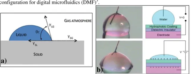
Fig. 1.1 – a) Illustration of the triphase contact line; b) Water drop over a hydrophobic surface. Top: without applied voltage (high contact angle). Bottom: with applied voltage (decrease in the contact angle value).3
b)
1.
I
NTRODUCTION
1.1
Electrowetting-on-dielectric (EWOD)
Electrohydrodynamic forces are responsible for the movement and control of liquid droplets1,2 and, as the name suggests, these operations occur by the presence of electric fields. In these devices, electro-capillarity effect, which arises from the distribution of free charge carriers between different phase media, can be designated electrowetting (EW). The applied electric field on a droplet that is in contact with a solid electrode acts on the triphase contact line (liquid droplet, gas atmosphere and solid hydrophobic lay-er), as illustrated in Fig. 1.1a. The free charge carriers in the droplet will then cause a contact angle reduction, i.e., wetting, that ultimately leads to droplet motion1. In order to
prevent the occurrence of electrolysis, a dielectric layer is inserted in between the drop-let and the electrode, leading to an increase in the actuation voltage. This is the most typical configuration of electrowetting, and it is designated by electrowetting-on-dielectric (EWOD) configuration (Fig. 1.1b.), which has become the most promising configuration for digital microfluidics (DMF)3.
1.2
Digital Microfluidics
Digital microfluidics, in a fundamental level, can be described as a liquid handling technique that allows a control over the movement of droplets, under the influence of electrical fields. DMF is a relatively recent field of studies, that shares some of the char-acteristics with microchannels based microfluidics, showing some interesting
vantages, in which one can refer the possibility of addressing individual reagents in a discrete way, i.e., independent of tubing networks4. The control of each droplet is made
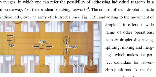
individually, over an array of electrodes (vide Fig. 1.2), and adding to the movement of
droplets, it offers a wide range of other operations, namely droplet dispensing, splitting, mixing and merg-ing5, which makes it a per-fect candidate for lab-on-chip platforms. To the fea-tures mentioned so far, re-duced volume is yet anoth-er charactanoth-eristic whanoth-ere DMF can offanoth-er advantages ovanoth-er othanoth-er techniques, since it is suit-able for nL to mL range in droplet volume, which can be translated to reagent reducing. Inclusively, fL droplet volume has already been reported in some studies, revealing this advantage of DMF6.
Due to the unique features this technology reveals, innumerous studies have been al-ready conducted to this date, in various fields, such as biology7,8, chemistry9,10 and med-icine11-13, to refer some examples.
The interest in this area started in the late 1970s, early 1980s, where it was demonstrated that the application of electric charge could produce a large variation in contact angle for water drops over Teflon (PTFE)14. However, it wouldn’t be until the XXI century that the field of DMF started to be further developed, mainly with the con-tributions of two different groups, i.e., Fair et al.15 and Kim et al.16,17, respectively. The
Fair group applied the concepts of electrowetting-on-dielectric and developed a proto-type where droplets with a volume in the range of microliters of a solution of KCl moved along an array of electrodes, with an average velocity of 30 mm/s, with the ap-plication of voltages in the range of 40-80 V15. Some years after, Kim’ group success-fully developed a system in which droplets not only moved, but performed some other fluidic operations, namely creating, transporting, cutting, and merging liquid drop-lets16,17. In fact, this was the first reference to the fluidic operations that involved not only the movement and merging of droplets, but also the dispensing operation, which Fig. 1.2 – DMF device, where the array of electrodes is presented.
Fluidic operations also observable. Adapted from 5.
represented at that time a very significant breakthrough towards lab-on-a-chip develop-ment using DMF.
Regarding the mechanisms of EWOD, it is worth to mention the limitations pointed out by some authors. Jebrail4, for instance, revealed some phenomenon that lack
expla-nation with the EWOD theory, namely the movement of droplets with low surface ten-sion, that don’t show variation in contact angle and contact angle saturation. Adding to that, some authors suggest that dielectrophoresis (DEP) should be complementary to EWOD approaches18-20, basically due to the fact that EWOD is only valid for conduc-tive and aqueous liquids until a certain threshold of frequencies and leaves out dielectric liquids, such as oils. As the application of the device to be designed is mainly the opera-tion of aqueous soluopera-tions, i.e., conductive liquids, EWOD understanding and
mathemat-ic modeling would be suitable for the optimization studies to be performed.
1.3
The role of the dielectric layer
The first devices designed for droplet motion were designed by the Fair group, where droplets in the range of microliters moved along an array of electrodes, with con-siderably high voltages, in the range of 40-80 V15. The device, consisted of a two-plate structure, where the patterned control electrodes were 2000 Å thick, coated with 7000 Å of parylene C and finally, as hydrophobic material, approximately 2000 Å of Teflon AF 1600. As for the top plate, the ground electrode was made of a transparent ITO, and also a thin layer of Teflon AF 1600, with 500 Å.
In order to improve the ease how droplets are actuated, a mathematic modeling and comprehension of the EWOD mechanism is required (limitations of this understanding are not to be considered, as mentioned previously). The motion of the droplets occurs by promoting a difference in contact angles by operation of voltage in each end of those droplets, by EWOD effect. In order to better understand the major contributing factors in the contact angle change phenomena, a derivation of Young’s equation (Equation 1) is performed to obtain the Lippmann–Young’s law5,21 (Equation 2):
𝛾𝛾𝑆𝑆𝑆𝑆 =𝛾𝛾𝑆𝑆𝑆𝑆+𝛾𝛾𝑆𝑆𝑆𝑆𝑐𝑐𝑐𝑐𝑐𝑐𝜃𝜃0 (1)
𝑐𝑐𝑐𝑐𝑐𝑐𝜃𝜃𝑉𝑉 =𝑐𝑐𝑐𝑐𝑐𝑐𝜃𝜃0+2𝜀𝜀𝛾𝛾0𝜀𝜀𝑟𝑟 𝑆𝑆𝑆𝑆𝑡𝑡 𝑉𝑉
2 (2)
where θV and θ0 are the actuated and non-actuated contact angles, respectively, γLG the surface tension between the liquid and the filler medium, 𝜀𝜀𝑟𝑟 the relative permittivity of the dielectric, 𝜀𝜀0 is the permittivity of free space, t the dielectric’s thickness, and V the
applied voltage. It can be deduced that the highest variation of the contact angle can be obtained by an increase of voltage, which implies highest amount of energy supplying, or an increase in relative permittivity of the dielectric, or yet a reducing in the dielec-tric’s thickness, which can potentiate disruptive breakdown of the dielectric layer. To be mentioned that this equation is basically a translation of electrowetting effect in a capil-lary force21, and that a great variation in contact angle is not a requirement for droplet
movement5, so these simplifications may be compromising in optimization.
Considering the first device mentioned to be able to perform all the fluidic opera-tions, developed by Kim’s group17, the choices for an optimized architecture, capable of performing all operations at 25 V, varied depending if it was a symmetrical or an asymmetrical structure. The symmetrical structure consisted in the top and bottom lay-ers being identical, where the dielectric material used was a 1000 Å thick silicon diox-ide covered with a 200 Å Teflon layer, the same for both plates. For the asymmetrical structure, the bottom plate remained unchanged, but in the top plate there was only a 200 Å Teflon layer.
Moon et al.22 proceeded in an attempt of lowering the voltages, following two dis-tinct approaches, in order to verify the relative importance of each one: employing ma-terials with higher dielectric constant and/or reducing the dielectric layer thickness, ba-sically reducing the figure of merit(𝑡𝑡/𝜀𝜀𝑟𝑟)1/2, which arises from the Lippmann–Young’s
law.
To verify the dielectric thickness effect on the EWOD voltage, various thicknesses of Teflon AF, silicon dioxide and parylene layers have been tested, being the last two coated with a 200 Å amorphous fluoropolymer layer. Regarding the effect of the dielec-tric constant, layers of similar thickness of silicon dioxide and barium strontium titanate (BST), coated with the same amorphous fluoropolymer have been studied22. In this study, BST coated with a 200 Å amorphous fluoropolymer layer revealed to be suitable for DMF applications, showing good results in nL scale water droplets driving with on-ly 15 V.
Li et al.23 suggested anodic tantalum pentoxide (Ta
2O5) as a good solution for
EWOD applications, for several reasons, namely the fact that this material can be pro-duced at room temperature by means of anodization and the possibility of driving drop-lets with relatively low voltages (14 V). It is also relevant the fact that this material is pinhole free, which allows for a good deposition of Teflon as a hydrophobic coating.
Ta2O5 dielectric constant is high, but inferior to BST’s, however, BST films have time
dependent breakdown problems, whereas Ta2O5 shows a more stable behavior.
In another attempt, Lin et al.24 showed the possibility of dispensing 300 pL droplets applying voltages of 11.4 V, using devices composed by a multilayer dielectric struc-ture, sputtered Ta2O5 and parylene-C, with a top-coating of Cytop. To obtain optimized
values for each deposited layer, several variables were studied, for different dielectric compositions. The process of electrode patterning was also relevant, since a two-level-metal fabrication was implemented, allowing for the fabrication of smaller and denser electrodes.
More recently, Chang et al.25 suggested a EWOD device with aluminum oxide as di-electric, deposited recurring to an atomic layer deposition (ALD) method. For this de-vice, a single-plate architecture was used, with a 1270 Å thick aluminum oxide layer, top-coated with Teflon-AF. By application of voltage between the actuation and refer-ence electrodes, 2 μL droplets were moved, being the minimum applied voltage of 3 V, which is one of the lowest values reported so far. However, it is also relevant to mention that this minimum voltage is not applicable for all the fluidic operations, as droplet dis-pensing, since this operation requires higher voltages, and, as mentioned before, single-plate structures are limited to driving and mixing operations.
One limitation pointed to the DMF conventional devices is the high cost associated to them. Khodayari et al.26 suggested a low-cost approach to this problem, using spin-coated fluoropolymer over an aluminum electrode. This method, that had been previ-ously attempted but without success due to layer defects, was improved by using a citric acid electrolyte and anodic voltages. The actuation voltages obtained are competitive with conventional methods, ca. 10 V, for the driving operation. This method may
con-tribute towards price reduction of this technology, and suitable for lab-on-a-chip plat-form.
A summary table with some of the various dielectric materials and compositions used in DMF up to this day may be consulted in the Appendix A.
2.
M
ATERIALS AND
M
ETHODS
2.1
Properties of the composing layers
There are some main criteria in order to define the materials composing the devices, from which the dielectric constant and dielectric strength are considered the most im-portant ones, but also the degree of step coverage, since the devices show patterned structures due to the electrodes, for instance. As these devices are applied for the movement of conductive liquids, it is of greatest relevance that the insulating layers are pinhole free.
In the view of the fact that parylene-C was used for the testing of the first digital mi-crofluidics devices15,16,22, even though being aware of its limitations concerning the
greater value of voltage required for droplet manipulation (due to higher values of the figure of merit(𝑡𝑡/𝜀𝜀𝑟𝑟)1/2, since the ε
r of parylene-C about 3), this material was chosen
for the development of the first devices. The choice of parylene-C was related to its fea-tures, such as the high dielectric strength (around 200 V/μm[2], however decreasing with the reduction of thickness), and the fact that it produces chemically inert, robust and pinhole free surfaces. In order to obtain a larger initial angle, a Teflon AF 1600 hydro-phobic thin layer (ca. 50 nm) is added, thus reducing the contact angle hysteresis2,25,27.
This material is also versatile in the way that it is chemically inert, so both acids and bases can be used as conductive liquids. Teflon AF is a fluoropolymer which could be used not only as a coating layer, but also as insulator. However, it shows dielectric breakdown when voltages inferior to those required to moving droplets are applied, and also polarity issues, so it is not used as insulator but rather just as hydrophobic layer22,28. With the objective of reducing the applied voltages, a high dielectric material is re-quired, such as tantalum pentoxide (dielectric constant around 23, and dielectric strength of approximately 800 V/μm[24]). The choice of this material had in mind not
only its intrinsic characteristics, but also the fact that the knowhow for obtaining good and uniform layers is present within CENIMAT and the Department of Material Sci-ences. This material, even though it reveals interesting dielectric properties, has shown pinhole issues that ultimately lead to a poor reliability, since higher voltages need to be applied for the device to maintain the droplet moving rate with time24, and so multilayer approaches using Parylene-C appear as a good option to join the best of both materials:
the high dielectric constant and strength of tantalum pentoxide, and the step coverage and robust, pinhole free surfaces determined by the Parylene-C. As mentioned in a pre-vious chapter, anodic growth of tantalum pentoxide produces supposedly pinhole free layers23, yet that technology was not available for testing, and so sputtering methods
were applied.
2.2
Device fabrication
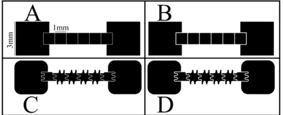
Digital microfluidic devices were fabricated in the facilities of CEMOP/UNINOVA, CENIMAT/I3N and at the Department of Material Sciences of the Faculty of Sciences and Technology of the New University of Lisbon. The patterning of the chromium elec-trodes composing the the bottom-plate was achieved implementing methods of photoli-thography and lift-off, obtaining a thickness around 200 nm. Polyester film masks on glass were used as photomasks, with two changeable factors, the shape of the electrode (squares or interdigital) and the electrode separation (30 or 50 μm). The size of ele c-trode was maintained, 1 mm2 for the moving electrodes, and 3 mm2 for the reservoirs (Fig. 2.1).
The patterned electrodes were then coated with different thicknesses of Parylene-C, using a vapor deposition system (Specialty Coating Systems - PDS 2010 LABCOAT-ER2). Concerning the layer of Teflon AF 1600 (DuPont), the thickness was maintained in all the depositions, and it is around 50 nm of Teflon-AF. For such, a solution of 0.6% wt/wt in Fluorinert FC-40 (DuPont) was spin-coated for 30 s at 1000 rpm, followed by a post-baking on a hot-plate for 10 min at 160oC.
As for the top-plate, glass substrates coated with ITO were coated with 50 nm of Teflon AF, with the method described above.
Fig. 2.1 – Patterning of the electrodes: A – Square electrodes with 30 μm gap between electrodes; B - Square electrodes with 50 μm gap between electrodes; C - Interdigital electrodes with 30 μm gap between electrodes; D - Interdigital electrodes with 50 μm gap between electrodes.
The separation between plates when the device is placed on the platform is ca.
100-150 μm, and it is composed by two or three layers of Kapton tape (DuPont).
For the devices produced with tantalum pentoxide, there is one extra step adding to the devices produced just with parylene-C, which is a sputtering process after patterning the electrodes. The sputtering of amorphous tantalum pentoxide was carried in an AJA International ATC 1300 sputtering system, in order to obtain 200 nm thick layers, over which different thicknesses of parylene-C were subsequently coated. To produce layers with the desired thickness, the power applied to the target was 100 W, and 15 W to the substrate, while having a reflected power of 0 W and a DCbias of 106 V. The deposition
was carried throughout 113 minutes, with a CL-CT maintained at 56/44.
Throughout the whole work, stylus profilometry was used to evaluate the obtained thicknesses of the different device’s layers, using an Ambios XP-Plus 200 Stylus pro-filometer.
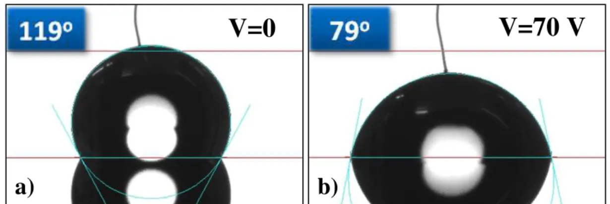
Fig. 3.1 – Contact angle measurements in a structure. The measurements were performed by
in-troducing a needle in a 5 μL droplet of DI water with a resistivity of 15 MΩ.cm: a) high initial co n-tact angle without voltage application, ≈118.8º; b) contact angle after applying 70 Vdc on the drop-let, obtaining a final contact angle of approximately 78.7º.
a)
b)
V=0
V=70 V
3.
R
ESULTS AND DISCUSSION
3.1
Electrowetting-on-dielectric and dielectric breakdown
As mentioned previously, this thesis focused on existing knowledge in the field of electrowetting-on-dielectric in order to design, produce and optimize new devices. This interfacial energy phenomenon, as the designation itself implies, is responsible for the effect of wetting, which is the reduction in the contact angle of a determined liquid over a surface. Typically, it is considered that contact angle reductions in the order of 40o are required for proper droplet manipulation2,22,23, and by so, the dielectric layer in combi-nation with the hydrophobic layer have to be designed in the interest to achieve a com-parable degree of contact angle reduction within a desired range of actuation voltages. In order to perform the EWOD tests, a modification in the contact angle measurement system was carried, by introducing a second needle next to the dispensing needle, which contained a wire inside, connected to a voltage generating system (see Appendix B).
The effect of EWOD is illustrated in Fig. 3.1, as part of the studies that allow us to better understand the effects of thickness and dielectric constant in contact angle reduc-tion through voltage applicareduc-tion, in this situareduc-tion, at 70 V. The used configurareduc-tion of 1.8
μm of parylene-C and 50 nm of Teflon hydrophobic coating enabled a contact angle reduction of over 40º. The presented images were obtained with Dataphysics OCA20 contact angle measurement system, equipped with a high-resolution CCD camera.
As referred, this test was part of a broader study which was conducted with the pur-pose of understanding the impact of some variations in the behavior of the devices. In
order to produce reliable and robust platforms, a theoretical study must be conducted to prevent some undesirable situations, such as dielectric breakdown at voltages under, or dangerously close, to those necessary to obtain an adequate degree of electrowetting (∆≈40º) to actuate droplets.
Examining the Lippmann–Young equation for electrowetting24,29 (Equation 2), one can observe that this phenomenon is controlled essentially by three factors: dielectric constant, thickness of the material and also the surface tension between the liquid and the filler medium. With the objective of further understanding how all this variables af-fect the device operation, a mathematical approach was performed with some key goals: directly comparing the theoretical actuation voltages for parylene-C layers with parylene/Ta2O5 multilayer; determine the minimum thicknesses to prevent dielectric
breakdown and compare the theoretical contact angle reduction with the experimental for some specific situations.
3.1.1Theoretical EWOD for parylene-C only and parylene/Ta2O5
multi-layer devices
In Fig. 3.2 several situations are illustrated, for EWOD and dielectric breakdown, varying the composition of the dielectric layer, thickness and filler medium.
When multilayer approaches are designed, considerably smaller voltages need to be applied in order to obtain high contact angle reductions while comparing with parylene-only dielectric layers. In the best theoretical scenario, a parylene-parylene-only device with 0.5
μm allows a contact angle reduction in air from 120º to 80º when applying 45 V, where-as the best theoretical scenario in a multilayer device, composed by 200 nm of Ta2O5
and 100 nm of parylene-C that degree of wetting is achievable with ca. 25 V. However,
this information shall not be separated from the one that the dielectric breakdown pro-vides, otherwise the obvious strategy would simply be reducing the layers, thus reduc-ing the actuation voltages. In practice, that strategy cannot be applied, as illustrated in Fig. 3.2 b) and d), since the required voltage for EW has to be inferior to the breakdown voltage, for functioning and reliable devices.
3.1.2Dielectric breakdown voltage
There are some particularities in the breakdown voltage study that require further detailing. In previous reports, the dielectric strength of parylene-C is stated to be around
200 V/μm24 when considering film thicknesses over 2 μm, but when scaling down, that
value decreases significantly due to pinhole defects. For modeling purposes, and keep-ing in mind that there was still much to understand about the vapor deposition system of parylene-C, the value of dielectric strength of this material was established for 40 V/μm, which introduces a safe margin that was considered to be adequate, and a contact reduc-tion from 120o to 70º was defined for all the presented situations. As for the multilayer
devices, it was developed what can be referred as an “equivalent dielectric strength”, for a structure with a fixed thickness of Ta2O5 of 200 nm, over which different thicknesses
of Parylene are coated. To develop this concept, the multilayer structure was regarded as a two-capacitors-in-series type of structure, and where the Parylene layer is the limit-ing factor, since its dielectric strength is considerably lower than the dielectric break-down of Ta2O5 (around 800 V/μm, according to previous studies of other authors24).
That explains why the curves for required voltage for EW in Fig. 3.2 d) only start at 200 nm. This concept is worth just to estimate the behavior of the multilayer devices, but it presents no physical correspondence, since it is a mathematical manipulation that has no match in the actual device physical operation.
The plotting for two types of filler medium, air and silicone oil will be further ad-dressed, since it is a critical feature of the system. Notwithstanding, it is possible to re-fer at this stage that varying the filler medium is an effective way of reducing the actua-tion voltages of DMF devices, but the applicability of this strategy is not always possi-ble, depending on some factors to be discussed ahead.
3.1.3EWOD experimental data vs. theoretical curves
Concerning the experimental plots shown in Fig. 3.2 a) and c), which were obtained using an adaptation of the system of contact angle measurement (see Appendix B), there is to refer that the dispensed droplets for obtaining each experimental value had the
vol-ume of 5 μL and a resistivity of 15 MΩ.cm. In every measure, different droplets were dispensed, to avoid introducing errors mainly related with droplet evaporation and charge trapping30,31, among others. The way how voltage is applied on the device is not to be disregarded, since there are reports of different behavior when applying the posi-tive terminal on the wire or in the device’s electrode22. The measurements were carried by applying the negative terminal on the wire and the positive terminal on the device’s electrode. Comparing the theoretical curve with the experimental data for the 1.8 μm
a)
b)
c)
d)
Fig. 3.2 – a) Theoretical EWOD effect for different thicknesses of parylene-C and a hydrophobic coating
of 50 nm Teflon AF 1600, and experimental plot for a 1.8 μm layer in air medium; b) Dielectric break-down of parylene-C with Teflon AF in silicone oil and air as filler mediums; c) Theoretical EWOD effect for different combinations of Tantalum pentoxide and parylene-C coated with 50 nm of Teflon AF 1600, and experimental plot for 200 nm Ta2O5 and 100 nm of parylene-C in air medium;d) Dielectric
break-down for different combinations of Tantalum pentoxide and parylene-C, in silicone oil and air as filler mediums.
Parylene-C device, there is a good matching up to 50 V, but above that voltage, for the 60, 70 and 80 V curves, the experimental data shows significant discrepancy with the theoretical curve, with contact angles inferior to the expected in a difference of approx-imately 10º. Considering the theoretical curve for 1 μm of Parylene-C in the same fig-ure, the experimentally acquired data seem to actually correlate more with this situation, yet exhibiting some noteworthy disparities. The gathered information support the con-clusion that the actual thickness of the device is not the expected one (1.8 μm), but ra-ther in the range of 1 – 1.8 μm, without greatly affecting the main objective of this study, which was studying the EWOD effect.
With respect to Fig. 3.2 c), the experimental plot seems to indicate a better correla-tion than the previously analyzed situacorrela-tion, but the discrepancies are still noticeable.
The theoretical-experimental differences in this situation, compared to the Parylene-only device, are more complex to analyze, since this device is multilayer composed. Nonetheless, one can assume that in this case, one, or both, of the layers are actually thicker than the predictions, which ends up by being a correct assumption, at least for the Ta2O5 layer, since the SEM images of devices produced with the same conditions as
the device used for the EWOD studies reveal that the Ta2O5 layer is in fact closer to 260
nm, rather than the expected 200 nm.
In both experimental plots there is an effect of saturation of the contact angle, which is more clearly visible in the multilayer device, and, although not so distinguishable, also in the Parylene-only device. This effect starts to occur when the wetting is in the range of 70-75º, sometimes for slightly higher contact angles. There are some reported attempts of explanations for the saturation effect, including charge trapping30,31 and electrostatic forces32, among others2,23. In some studies, it is even suggested a connec-tion between the effect of contact angle saturaconnec-tion and dielectric breakdown strength31,33.
3.1.4Frequency effect
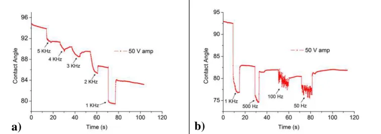
The studies on EWOD were also useful in the understanding of the signal’s frequen-cy influence on the contact angle variation. When using the EWOD phenomenon on DMF devices, the application of direct current causes the device to disrupt more easily, mainly due to electrolysis effects. Knowing that effect, alternate current is preferable, but the spectrum of applicable frequencies is limited and needs to be defined, depending not only on the characteristics of the liquid, but also in the characteristics of the dielec-tric layer composing the DMF device. To accomplish the objective of observing the fre-quency effect, a study was carried out and the results are shown in Fig. 3.3. In this study, a 2 μL DI water droplet with resistivity of 12 MΩ.cm was dispensed and a 50 Vrms voltage was applied, varying the frequency. In Fig. 3.3 a), the frequencies used
were 5, 4, 3, 2 and 1 kHz, whereas in Fig. 3.3 b) lower frequencies were applied, 1 kHz, 500, 100 and 50 Hz. The initial contact angles are much lower than the ones presented for EWOD using dc signals, since this device was only composed by the metal electrode and a 3.6 μm layer of Parylene-C, missing the hydrophobic coating of Teflon. For the case illustrated in Fig. 3.3, the frequencies that exhibit a higher degree of wetting are the 1 kHz and 500 Hz, and so it is possible to infer that these frequencies would be the most
suitable ones for a system in which the liquid and the dielectric layer would be similar to the ones studied. For higher frequencies, given that liquids are not perfect conductors, there is a limit for ion movement, and at a critical value, where the liquid goes from conductive to capacitive. This critical frequency is essentially given by the Equation 3, as reported by elsewhere2:
𝜔𝜔
c=
𝜀𝜀𝜎𝜎1𝜀𝜀10(3)
In this equation, 𝜔𝜔c represents the critical frequency, 𝜎𝜎1 the conductivity of the liquid and 𝜀𝜀1 the dielectric constant of the liquid. Since it was not the main objective of this thesis, this topic did not get further investigation, but in future studies it is advised to use different droplets for the measurements of each frequency, reducing the charge ef-fects, and also using liquids with different conductivities. Some other aspects, such as the characteristic time constant for charge relaxation2, that deals with the limitations imposed by the dielectric composition of the device, were not further investigated for not being considered essential, but in future optimization attempts, this characteristic may be considered.
3.2
Dielectric tests with parylene-C and Ta
2O
5Even though there is a lot of bibliography concerning the topic of dielectric studies and applications for parylene-C and tantalum pentoxide, it was considered that given the
b)
a)
Fig. 3.3 – Effect of applied frequency in EW, considering a fixed value of voltage (sinusoidal wave with 50 V of
amplitude), for a 2 μL DI water with resistivity of ca. 12 MΩ.cm. The effects of volume loss and contact angle hysteresis are not to be disregarded. These tests were performed on a layer of Parylene C without any hydro-phobic coating, hence the lower initial contact angle (ca. 93-95o) comparing to the ones verified when this type of coatings are present (ca. 120o).
matter of the undergoing work, a study of the developed layers would still be of utmost interest to better understand the respective characteristics.
For the realization of these tests, initially it was used the structure depicted in Fig. 3.4 a), which was later replaced by a different type of structure, represented in Fig. 3.4 b), provided that parasite capacitance effects were detected in the initial structure, aris-ing from the designed matrix configuration. Nevertheless, by operataris-ing some modifica-tions it was still possible to obtain reasonable capacitance values with these devices,
detailed in the Appendix F section. The improved structure for dielectric tests consisted of a line of aluminum, deposited on glass, with dimensions of 3 x 20 mm, over which it was then deposited the dielectric material, leaving an uncovered area of aluminum that would operate as bottom electrode, and ultimately another line of aluminum, deposited with an orientation of 90º from the bottom electrode. This structure can be considered as a simple parallel-plate capacitor, where the considered area is the electrode overlap of approximately 9 mm2. Silver ink was applied in an area above each electrode that does not overlap in order to connect a small wire to connect the test probes, as seen in Fig. 3.4b).
3.2.1Parylene-C dielectric tests
The dielectric layer of parylene-C was the one that required special care throughout the whole studies, since its specifications and particularities were fairly unknown inside the group. With time, it was possible to recognize an important role of the process pres-sure, since DMF devices produced with higher process pressures for the same thickness showed a proneness to disrupt with lower voltages. At some point, it was decided to
b)
a)
Fig. 3.4 – Developed structures for the dielectric tests: a) Matrix structure for the dielectric test of Ta2O5, responsible for the distinguishable brown tone; b) Cross structure for the
die-lectric test of parylene-C.
a)
b)
Fig. 3.5 – a) Capacitance measurements of a 550-600 nm Parylene-C layer for a range of 100 Hz to 100 kHz; b)
Loss tangent, or dielectric loss, experimental plot obtained for the measurements on the Parylene-C layer for a range of 100 Hz to 100 kHz.
keep the process pressure, independently of the desired thickness, in order to obtain more stable and reliable layers, and to be able to understand the effect Parylene-C dim-mer mass in the final film’s thicknesses.
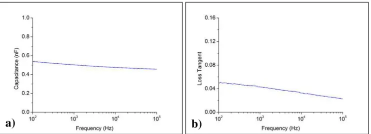
The dielectric tests presented in Fig. 3.5 correspond to a structure composed by a layer of approximately 550 nm of Parylene-C.
The capacitance measurements over frequency show a predictable behavior, as it slightly decreases with frequency. For the presented measurements, the obtained capaci-tance value at 100 Hz was 0.54 nF, whereas at 100 kHz the measured capacicapaci-tance was 0.46 nF.
When confronting the experimental data with the theoretical values of capacitance, a fairly accurate match was obtained. As mentioned previously, bibliography for Parylene-C presents a value of εr for this material of 3. Considering a parallel-plate ca-pacitor with an area of 9 mm2, with 550 nm of Parylene-C, the theoretical value for the
capacitance is 0.43 nF. Assuming the referred measured capacitance value at 100 Hz, a factor of approximately 1.24 is identified in the ratio between experimental and theoret-ical values. Doing the inverse exercise, considering the experimental values obtained, and keeping the area of 9 mm2, with 550 nm of Parylene-C, the experimental εr for this Parylene-C layer would be approximately 3.7. While considering the frequency of 100 kHz, for the same parallel-plate capacitor characteristics, the ratio experi-mental/theoretical capacitance values drops down to 1.05, providing an experimental εr of 3.15, closer to the reported dielectric constant value of 3.
It is relevant to mention that the capacitance tests that were carried out had not the sole purpose of confirming the dielectric constant of the material, but also its behavior with frequency, since the devices developed with these dielectric materials are supposed to operate in a broad range of frequencies, in order to perform the most diverse opera-tions, like impedance measurements with several signals of different frequencies. With the obtained results, it is possible to observe that this material suits that criterion, since the capacitance decay is not severe considering a relatively broad range of frequencies.
The loss tangent, illustrated in Fig. 3.5 b), is the tangent of the loss angle of value δ, which is basically the deviation relatively to π/2 between the applied voltage and the resulting current. This loss tangent ideally would be 0, for the case of a perfect dielec-tric, but since there is always a non-ideal component, a portion of the current will be in phase with the applied tension. For the dielectric in study, the dielectric loss tangent takes values between ca. 0.02 and 0.05 for a frequency range of 100 Hz up to 100 kHz,
which can be considered an acceptable value range of loss tangent.
3.2.2Tantalum pentoxide dielectric tests
Tantalum pentoxide started to be considered in a later phase of the DMF studies, af-ter it was possible to fulfill all the main objectives for Parylene-C as the only dielectric composing the devices. The deposition of this material, as previously mentioned, is per-formed by sputtering, and not by chemical vapor deposition, as it is for Parylene-C. For the purpose of dielectric study of this material, no multilayers were produced, but rather a study of Ta2O5 alone.
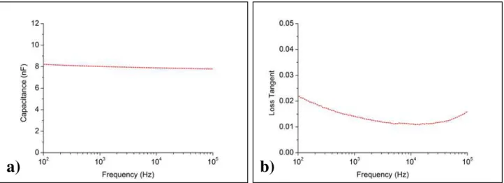
The initial dielectric tests performed on this material weren’t conclusive, by the same parasite effects that were also revealed in the Parylene-C studies. By modifying the structure in the same way as for the Parylene-C studies, it was possible to extract the experimental data for the dielectric tests with a layer of approximately 250 nm of Ta2O5,
plotted in Fig. 3.6.
Fig. 3.6 – a) Capacitance measurements of a 250 nm Ta2O5 layer for a range of 100 Hz to 100 kHz; b) Loss
tan-gent, or dielectric loss, experimental plot obtained on the 250 nm Ta2O5 layer for a range of 100 Hz to 100 kHz.
b)
a)
Regarding the capacitance curve (Fig. 3.6 a), decay with frequency is noticeable, as it was previously observed for the Parylene-C, but again, the decay is not very signifi-cant. Considering the range between 100 Hz and 100 kHz, the capacitance varies be-tween 7.8 and 8.2 nF, considerably superior to the obtained values for Parylene-C (over an order of magnitude). When comparing with the theoretical values, the value of ca-pacitance appears higher than estimated, in view of the fact that for a capacitor with the produced characteristics (area of 9 mm2, thickness of 250 nm and dielectric constant of 23) the capacitance should be approximately 7.3 nF. When comparing with the closest experimentally acquired capacitance value, within the considered range, of 7.8 nF, there is a factor of slightly over 1.06 in the ratio between experimental and theoretical values, that would translate in a dielectric constant of 24.4, maintaining the thickness of 250 nm of Ta2O5, and an area of 9 mm2. Considering the highest measured capacitance value of
8.2 nF, the ratio increases slightly to 1.12, for an experimental dielectric constant of ap-proximately 25.8. In what refers to the capacitance stability with frequency, one can verify that, as it happened with Parylene-C, this material shows a stable behavior for the 100 Hz to 100 kHz range, where no dielectric relaxation effects are present. Concerning the loss tangent, Ta2O5 also shows acceptable values of loss, in the considered range,
with a minimum of 0.01 and a maximum of 0.02, even better than the ones observed with Parylene-C. With these results, it is possible to conclude that the produced layers represent a viable solution for application as dielectric layer, only requiring further
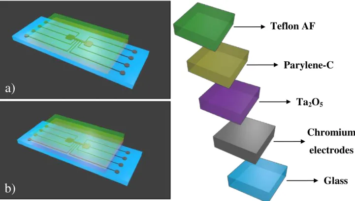
Teflon AF
Parylene-C
Ta
2O
5Chromium
electrodes
Glass
Fig. 3.7 – Device’s bottom plate architecture: a) Parylene-C as single dielectric covered with Teflon (not to scale); b) Multilayer dielectric structure, with Ta2O5 covering the electrodes, followed by Parylene-C and Teflon (not to
scale).
a)
b)
vestigation on why the theoretical and experimental values of capacitance differ in the way they currently do.
3.3
Device structure and operational conditions
3.3.1Structural analysis
At this point, knowing the most important characteristics of the dielectric layers to be used in the DMF devices, a structural analysis of the device is to be presented.
As depicted in Fig. 3.7, the produced devices are composed by several layers, and each of those layers is produced applying different methods. To observe directly the dif-ferent composing layers, SEM images for a multilayer device, ideally with 200 nm of Ta2O5 and 650 nm of parylene-C, were collected, as shown in Fig. 3.8.
Chromium
electrode
Glass
Parylene-C
Ta
2O
5b)
a)
Fig. 3.8 – Device’s layered structure images acquired with SEM, after milling a select area on a reservoir elec-trode recurring to FIB: a) different composing layers of the device, excepting the Teflon layer, which is harder to observe due to its dimensions (ca. 50 nm, as previously mentioned); b) detail to show the thicknesses of the deposited layers on glass: chromium – ≈390 nm; Ta2O5 – ≈260 nm and Parylene-C – ≈715 nm.
Taking a closer look on the information provided by the SEM images, and compar-ing it with the previous mentioned values for each layer’s thicknesses, there are some substantial deviations that require further understanding, since these deviations have a direct impact in the system specifications, implying, for example, higher actuation volt-ages, due to an increase in the figure of merit (𝑡𝑡/𝜀𝜀𝑟𝑟)1/2.
Starting with the chromium electrodes, the measured thickness for this layer was ap-proximately 400 nm, which is the double of what was intended to deposit. This devia-tion may arise of some calibradevia-tion issues in the system that indicates the deposidevia-tion growth rate and overall deposited material connected to the e-beam deposition tech-nique. This significant deviation, when dealing with parylene-C as single dielectric, may not be a determinant factor to the device’s operation, since when it comes to use parylene-C as single dielectric, and as it was already detailed in a previous chapter, the layers to be deposited are significantly thicker than in multilayer devices, and so, step coverage, which is one of parylene-C’s most well-known and explored characteristics, allows the device to operate normally. However, when dealing with materials like
Ta2O5, step coverage does not occur so easily, and given that the thickness of the
elec-trodes is substantially higher than the Ta2O5 layer (390 vs. 260 nm), in the space
be-tween adjacent electrodes, defects are more likely to appear. These predictable defects, though covered with parylene-C, may be the cause of some droplet moving difficulties, that at a first glance were solely attributed to electrode shape and spacing.
Regarding the Ta2O5 layer, the deposition parameters used to obtain the desired
thickness of 200 nm revealed to be inaccurate, since the obtained deviation is consider-able (30% above the desired thickness). Since this degree of deviation cannot be at-tributed just to process statistical error, further calibration studies are advised, because in the range of thicknesses at use, variations of this magnitude may represent a serious drawback in the device’s successful operation and attempt of lowering the applied volt-ages.
The parylene-C layer shows a higher thickness than the expected (10% more), even though there had been a great afford in trying to understand how the different process variables conjugate to obtain a specific thickness. In fact, despite the simplicity of the deposition technique, several factors need to be controlled to produce similar layers, not only the dimmer mass and process pressure, but also the position inside the deposition chamber, since there is a significant gradient of thicknesses along the three trays that compose the substrate holder, and as regarded in the dielectric tests, even in the same substrate there is a thickness gradient. For increased reproducibility of the layers, the position along the trays should be maintained. Again, further understanding for this ma-terial is advised, not only in order to develop new improved single dielectric devices with this material, but also to produce new multilayer devices with better specifications and lower thickness deviations, which is critical when the layers to be deposited scale down to few hundreds of nanometers.
3.3.2Further device specifications
The complete device, composed by bottom and top-plate, mounted in the platform produced for this effect, is shown in Fig. 3.9.
Fig. 3.9 – Complete device and test platform. This platform allows for the test of devices with up to 32 elec-trodes, as it is observable by the number of addressing voltage pins. The top-plate electrode is connected to ground voltage by the represented red cable. The Kapton tape spacers between bottom and top-plate are also visible.
Fig. 3.10 – Interdigital shape of electrodes and de-tail to exhibit the areas that facilitate the droplet movement.
In order to produce reliable and operational devices to perform tests, there were sev-eral concerns which were not directly related with the dielectric layer that also required some attention, and without which the device functionality would be compromised. Those issues can be summarized as shape, size and spacing of electrodes; filler medium and spacing between bottom and top-plate, presented as follows.
3.3.2.1Shape, size and spacing of electrodes
As it was presented in a preceding chapter, initially two different types of trodes’ shapes were designed: interdigital and linear. Although an interdigital elec-trodes’ shape would be more adequate for moving the droplets, since it would be easier for the droplets to be affected by neighboring electrodes’ electric fields, as it is made clearer in Fig. 3.10, in prac-tice that approach proved to be harder to implement than originally expected. Considering the lithography processes used to produce the electrodes, when per-forming the operation of lift-off a lot of defects occurred in the areas where
trodes interconnect, and so the final yield of production was considerably low compar-ing to the square shaped electrodes. That could be solved by uscompar-ing different etchcompar-ing methods instead of lift-off or by using more adequate, even though more expensive, masks (e.g. chromium on glass masks), but there is also another issue which is not
relat-ed with the production methods, but rather the tests themselves. When performing tests with devices composed by interdigital electrodes, it was observed that disruption of the devices always started at the fine edges of the interdigital electrodes, which may be ex-plained by non-uniformities in the electric fields’ distribution along the electrode, being more intense in the fine edges, and so more prone to disruption. Considering these ef-fects, the squared shape electrodes were preferred over interdigital, even though electric field in this type of electrodes is still non-uniform, the disruption effect is not so signifi-cant.
As for the size of electrode, the choice was for 1 mm2 square electrodes, although there are to this day reports of electrodes in the micron range. This choice was based on the fact that the devices were being manufactured for the first time, and so the observa-tion of the funcobserva-tioning of the devices had to be carried initially in a naked-eye scale. In the future a downscaling is a possible development and will allow for the reduction of reagents’ volume, if necessary.
When it comes to electrode spacing, 30 and 50 μm masks were designed, but co n-sidering that the choice rested on squared electrodes, 30 μm of spacing was defined as standard spacing, in an attempt to balance the fact that there is no crossing between ad-jacent electrodes, as in the interdigital design. That spacing can and shall be reduced in future developments, since for the time that was not possible, given the fact that the masks with that spacing dimensions are much more expensive than the ones effectively used, with much lower associated costs.
3.3.2.2Filler medium
In Section 3.1, dielectric breakdown curves were plotted for two different types of filler medium: air and silicone oil. Filler medium is basically the medium in which the droplet is placed on the device, between bottom and top-plate. Revisiting the Lippmann-Young equation (cos θV= cos θ0+ε0εr
2γt V2), the term γ corresponds to the surface ten-sion between the liquid and the filler medium, and by decreasing this parameter, lower actuation voltages are required to perform fluidic operations with droplets. Apart from