Pedro Miguel Nunes Mendes
Licenciado em Ciências da Engenharia Electrotécnica e de Computadores
Random Number Generator
based on Ring Oscillators
for IoT applications
Dissertação para obtenção do Grau de Mestre em
Engenharia Electrotécnica e de Computadores
Orientador: Doutor João Palma Goes, Professor Associado, Faculdade de Ciências e Tecnologia
da Universidade Nova de Lisboa
Júri
Presidente: Doutor Rui Morgado Dinis, Professor Associado - FCT/UNL Arguente: Doutor Luís Santos Gomes, Professor Associado - FCT/UNL
Random Number Generator based on Ring Oscillators for IoT applications
Copyright © Pedro Miguel Nunes Mendes, Faculdade de Ciências e Tecnologia, Universi-dade NOVA de Lisboa.
A Faculdade de Ciências e Tecnologia e a Universidade NOVA de Lisboa têm o direito, perpétuo e sem limites geográficos, de arquivar e publicar esta dissertação através de exemplares impressos reproduzidos em papel ou de forma digital, ou por qualquer outro meio conhecido ou que venha a ser inventado, e de a divulgar através de repositórios científicos e de admitir a sua cópia e distribuição com objetivos educacionais ou de inves-tigação, não comerciais, desde que seja dado crédito ao autor e editor.
Este documento foi gerado utilizando o processador (pdf)LATEX, com base no template “unlthesis” [1] desenvolvido no Dep. Informática da FCT-NOVA [2].
A c k n o w l e d g e m e n t s
I would like to acknowledge the contributions of a number of people who were very helpful and supportive in my research.
I extend my sincere appreciation to my principal advisor, Professor João Goes, whose wisdom and expertise enabled the successful completion of this research. Would like to extend my gratitude to Professors Anikó Costa, Filipe Moutinho, Ricardo Madeira and Raul Rato for the help on the development of this Thesis.
Thanks to Ihor Vasyltsov for the support and helpful advices, which significantly increased the quality of this project.
To my parents and my sister who always supported me during my journey and gave me all the tools without ever giving up on me.
A special thank you to Daniela Prudêncio, for all her love and support during the most difficult times.
Finally I wanted to thank all my friends who helped me during all these years and who always lifted me up during the academic journey.
A b s t r a c t
Since the beginning of times that human beings were presented with the difficult
of protecting their data. In all wars, cryptographic systems where essential to wining. Nowadays, fighting global terrorism makes cryptography of paramount importance in communication and security of critical systems. Cryptographic methods present a real challenge, so hard that it is as difficult to create as it is to crack.
Since the first appearances of Integrated Circuits, methods have been created to pro-tect the data on them, the same happened when the first networks appeared and nowa-days we still face the same challenge. Centuries have passed and the definition of the random word still creates confusion when trying to define it. This thesis proposes a ran-dom generation method which proved to be effective according to worldwide standards
with the new emerging technologies of the IoT in mind.
A True Random Number Generator (TRNG) based on ring oscillators, implemented in a Field Programmable Gate Array (FPGA) platform is proposed and evaluated. Based on some new concepts on ring oscillators, jitter noise was analysed and used as a main noise source to create randomness.
The main aim of this project was to investigate and develop of a secure system that met the international requirements for IoT purposes.
R e s u m o
Desde o inicio dos tempos, os seres humanos defrontam-se com o desafio de proteger informação. Em todas as guerras, os sistemas criptográficos são essenciais para vencer. Hoje em dia, tendo em conta o terrorismo global que enfrentamos, a criptografia é um assunto de extrema importância na comunicação e na segurança de sistemas críticos. Os métodos criptográficos apresentam assim um desafio real, tão difícil de criar como de decifrar.
Desde o aparecimento dos primeiros Circuitos Integrados, foram criados métodos para proteger os dados que estes tratam, o mesmo aconteceu quando surgiram as primeiras redes e, hoje em dia, ainda enfrentamos o mesmo desafio com o aparecimento de novas tecnologias.
Os séculos passaram e a definição da palavra ‘aleatório’ ainda cria dificuldades em quem a tenta definir ou medir. Esta tese propõe um método de geração de números aleatórios que se mostrou efetivo de acordo com padrões mundiais e com o objetivo de aplicação nas novas tecnologias da IoT em mente.
Um verdadeiro gerador de números aleatórios (TRNG) baseado em osciladores de anel, implementado através de uma plataforma FPGA é proposta e avaliada. Com base em alguns novos conceitos sobre osciladores de anel, o ruído jitter foi analisado e usado como fonte principal incerteza para gerar aleatoriedade nos resultados.
O principal objetivo deste projeto foi investigar e desenvolver um sistema seguro que atendeu aos requisitos internacionais de segurança para aplicações em tecnologias da IoT.
C o n t e n t s
List of Figures xvii
List of Tables xix
Listings xxi
Acronyms xxiii
1 Introduction 1
1.1 Introduction . . . 1
1.2 Problem Statement . . . 2
1.3 Goals . . . 2
1.3.1 Unpredictability. . . 3
1.3.2 Scalability . . . 4
1.3.3 Consistency . . . 4
1.4 Thesis’ Outline . . . 4
1.5 Main contributions . . . 5
2 State of the Art 7 2.1 RNG Basics . . . 7
2.2 Basic RNG Architecture. . . 8
2.2.1 Noise Sources . . . 9
2.2.2 Sampling . . . 10
2.2.3 Post-processing . . . 10
2.2.4 Output interface. . . 10
2.3 Previous RNG’s works . . . 11
2.3.1 Noise Amplification RNG . . . 11
2.3.2 Three Stage Noise Amplification RNG . . . 11
2.3.3 SiN MOSFET Ph-RNG . . . 12
2.3.4 Linear Feedback Shift Register RNG . . . 13
2.3.5 Ring oscillator RNG’s . . . 15
2.3.6 Arbiter physical unclonable function . . . 18
CO N T E N T S
3.1 Hardware . . . 21
3.1.1 Spartan 3 FPGA board UG130 . . . 21
3.1.2 Oscilloscope . . . 22
3.2 Cryptography using FPGA’s . . . 22
3.3 Ring oscillator TRNG design . . . 23
3.4 Ring design and properties . . . 23
3.4.1 Rings’ length. . . 24
3.4.2 Placement of the rings . . . 25
3.4.3 Jitter and Phase noise analysis . . . 28
3.4.4 Ring oscillator topology . . . 32
3.5 Entropy source and sampler . . . 35
3.5.1 ROs data analysis . . . 37
3.5.2 Jitter analysis on multimode ring oscillators . . . 40
3.6 Post-processing techniques . . . 45
3.6.1 XOR Corrector Vs Von Neumann Vs Truncation of defective bits . 45 3.7 Interface . . . 46
3.7.1 UART block . . . 46
3.7.2 Counter . . . 48
3.7.3 8-bit shift register . . . 48
3.8 Final design . . . 48
4 Statistical tests and analysis 51 4.1 FIPS140-1 tests . . . 52
4.1.1 Long run . . . 52
4.1.2 Mono-bit test . . . 52
4.1.3 Poker test. . . 52
4.1.4 Runs test . . . 52
4.2 NIST test suite . . . 53
4.2.1 NIST Test Concepts . . . 55
4.2.2 Frequency test . . . 57
4.2.3 Frequency test within a block . . . 58
4.2.4 Runs test . . . 58
4.2.5 Discrete Fourier Transform (spectral) test . . . 59
4.3 AIS.31 in BSI test suite . . . 61
4.3.1 AIS.31 certification . . . 62
4.3.2 Class P1 . . . 63
4.3.3 Class P2 . . . 63
4.3.4 T7 - Multinomial distribution test. . . 64
4.3.5 T8 - Entropy Test . . . 64
4.4 Extraction method . . . 64
4.5 Test Results. . . 65
CO N T E N T S
4.5.1 FIPS140-1 on the Cryptool . . . 66
4.5.2 NIST test suite . . . 67
4.5.3 AIS.31 on BSI test suite . . . 68
4.6 Comparison . . . 69
5 Conclusions 73 5.1 Future Work . . . 74
Bibliography 75
I Annex 1 - SCH and VHDL Files 79
L i s t o f F i g u r e s
1.1 Statistical Independence . . . 4
2.1 RNG type and implementation . . . 7
2.2 RNG Noise Classification . . . 8
2.3 RNG general Architecture . . . 9
2.4 Noise Amplification RNG Circuit Schematic . . . 11
2.5 Noise Amplification RNG proposed by [23] . . . 12
2.6 SiN MOSFET RNG proposed by [20] . . . 13
2.7 LFSR RNGnbit . . . 14
2.8 Tkacik LFSR CASR TRNG design . . . 14
2.9 Ring oscillator RNG design . . . 15
2.10 Ring oscillator TRNG design proposed by [32] . . . 16
2.11 FIRO design . . . 16
2.12 GARO design . . . 16
2.13 Metastability RO. . . 17
2.14 3-edge RO proposed by [42] . . . 17
2.15 Delay implementation for Arbiter PUF’s . . . 18
2.16 Arbiter PUF with Oscillators [31] . . . 19
3.1 Ring oscillator with enable signal . . . 24
3.2 Ring oscillator 7 inverters . . . 25
3.3 Ring oscillator 101 inverters . . . 26
3.4 Manual placement test for higher delay. . . 26
3.5 Ring oscillator with 7 inverters in a specific placement for maximum delay . 27 3.6 RO with 101 inverters manual placement . . . 27
3.7 Jitter noise classification . . . 28
3.8 Cycle-to-cycle jitter . . . 29
3.9 Phase noise per unit bandwidth . . . 30
3.10 Jitter wizard on manual placed design with 7 delay stages . . . 30
3.11 Jitter wizard on auto placed design with 7 delay stages . . . 31
3.12 Jitter wizard on manual placed design with 101 delay stages . . . 32
3.13 Jitter wizard on auto placed design with 101 delay stages . . . 33
L i s t o f F i g u r e s
3.15 Ring placement on far apart and close interaction . . . 34
3.16 Waveform comparison between RO spacing . . . 35
3.17 Final entropy source block and sampler . . . 36
3.18 Pulse generator . . . 36
3.19 Final ROs placement . . . 37
3.20 FFT of the RO output . . . 38
3.21 FFT of the XOR RO output . . . 38
3.22 FFT of the Entropy source output . . . 39
3.23 Graphical representation of the autocorrelation . . . 39
3.24 Autocorrelation on XOR output of two ROs of different lengths . . . . 40
3.25 Jitter analysis on the length 9 Multimode Ring . . . 41
3.26 Jitter analysis on the length 13 Multimode Ring . . . 42
3.27 Jitter analysis on the length 15 Multimode Ring . . . 43
3.28 Jitter analysis on the length 21 Multimode Ring . . . 44
3.29 Block diagram of a full interface block . . . 46
3.30 UART Frame . . . 47
3.31 UART Transmitter . . . 47
3.32 8Bit Shift Register . . . 48
3.33 Final TRNG schematic . . . 49
3.34 Final TRNG schematic without PP . . . 49
3.35 Final system placement on the FPGA . . . 49
4.1 NIST Test suite terminal application . . . 54
4.2 Graphical representation of ERFC function . . . 55
4.3 Graphical representation of normal distribution. . . 56
4.4 Graphical representation ofχ2distribution with the different degrees of free-dom . . . 56
4.5 Graphical representation ofpvalue . . . 57
4.6 DFT Example in [26] . . . 60
4.7 BSI Test Suite Application . . . 62
4.8 Extraction of Random Numbers with TeraTerm through UART . . . 65
4.9 Histogram on multiple Long Sequences. . . 65
4.10 Long Sequence DFT Analysis . . . 66
4.11 FIPS140-1 Tests with Cryptool V1.2.31 . . . 66
4.12 Vitanyi Graph on multimode XOR design with Cryptool . . . 70
4.13 Vitanyi Graph on [33] with Cryptool . . . 70
4.14 Linux Entropy RNG . . . 72
4.15 Linux Entropy RNG Histogram . . . 72
I.1 Pulse Generator SCH . . . 83
I.2 Multi RO Length 9 SCH . . . 84
L i s t o f Ta b l e s
2.1 Three Stage RNG Performance Table . . . 12
3.1 XOR Truth Table . . . 23
3.2 XOR Multi input Truth Table . . . 23
3.3 Standard deviation on multimode RO design . . . 44
3.4 Von Neumann Corrector Rule . . . 45
3.5 XOR Corrector Rule . . . 46
3.6 Device utilisation summary with PP . . . 50
3.7 Device utilisation summary without PP . . . 50
4.1 FIPS140-1 Runs test approval . . . 53
4.2 Changes between FIPS140-1 and FIPS140-2 . . . 53
4.3 Changes between FIPS140-1 and FIPS140-2 on Runs Test . . . 53
4.4 NIST statistical tests. . . 67
4.5 BSI statistical test results on FIPS140-1 . . . 68
4.6 BSI statistical test results on FIPS140-2 . . . 68
4.7 NIST statistical tests on [33] with post-processing . . . 69
4.8 NIST statistical tests on [33] and our project without post-processing . . . . 71
L i s t i n g s
4.1 Matlab Sketch Spectral Test . . . 61
I.1 LogicGate.vhdl. . . 79
I.2 Ro3instance.vhdl . . . 79
I.3 RO9.vhdl . . . 80
I.4 Vneuman.vhdl . . . 81
A c r o n y m s
A/D Analog to Digital.
ADC Analog to Digital Converter.
ASIC Application Specific Integrated Circuit.
BSI Bundesamt in der Informationstechnik.
CASR Cellular Automata Shift Register.
CCO Current Controled Oscillator.
CLB Configurable Logic Block.
DAS Digitised Analog Signal.
DC Direct Current.
DFT Discrete Fourier Transform.
FFT Fast Fourier Transform.
FIPS Federal Information Processing Standards.
FIRO Fibonnaci Ring Oscillator.
FPGA Field Programmable Gate Array.
AC R O N Y M S
HEX Hexadecimal.
HPF High Pass Filter.
I/O Input/Output.
IC Integrated Circuit.
IoT Internet of Things.
JTAG Joint Test Action Group.
LFSR Linear Feedback Shift Register.
LUT LookUp Table.
NIST National Institute of Standards and Technology.
PDF Probability Density Function.
PP Post-Processing.
PRNG Pseudo Random Number Generator.
PUF Physical Unlonable Function.
RAM Random Acess Memory.
RNG Random Number Generator.
RO Ring Oscillator.
RS232 Recommended Standard 232.
S/H Sample and Hold.
AC R O N Y M S
SCH Schematic.
SOC System On Chip.
SR Shift Register.
TRNG True Random Number Generator.
UART Universal Asynchronous Receiver/Transmitter.
USB Universal Serial Bus.
VHDL VHSIC Hardware Description Language.
C
h
a
p
t
e
r
1
I n t r o d u c t i o n
1.1 Introduction
The science of hiding any kind of information is called cryptography. This secret intel can make you loose a war for your enemy and, therefore, protecting data must be paramount importance. This document provides a tool for cryptographic systems, namely, a true random number generator.
Some of the most asked questions regarding this matter are
’what is actually random?’
or
’what means to be random ?’
, random can be considered as something that has always the same chance of happening. Consider a toss of a coin, if the coin is perfect and completely symmetric then every time it is tossed into the air there is a chance it could drop heads or tails. Always the same chance. But this ’random-ability’ has been a widely discussed topic since many centuries and how it can be evaluated and distinguished as ’random’ and ’not random’. Also, how can a result be quantified as more random than other. All of these examples and questions appeared when we were creating and developing this system.
Based on the fact that our system outputs binary sequences, ’1’ or ’0’, therefore, it can be considered as an analogy to the coin toss example, to be considered as random it has to present always the same change for each of the outcomes [19].
C H A P T E R 1 . I N T R O D U C T I O N
Nowadays, most of the security systems available are encrypted relying on software, consequently, there are a lot of random number generation algorithms made available for different applications. These usually are the so called Pseudo Random Number Generator
(PRNG), they are composed by complex algorithms which can generate ’almost’ random numbers, they present a real challenge to decrypt however sometimes it is possible to predict values, those systems present results that seems to be random but they are not, creating the possibility to hack them. This possibility, is something that its mandatory to be eliminated.
Returning to the same coin example, imagine a coin being tossed 50 times into the air, the first toss dropped heads where all the others tosses dropped tails, the coin tosser claims the probability of the toss is the same for both coin faces and asks you to guess which face will drop next. What would you answer ?
Random is something in which we can not find patterns:
’... this way, random is different from arbitrary, arbitrary does not imply a determinable distribution of probability like random’ [8]
By its interpretation, random presents the need to a distribution, therefore, do we need arbitrary sequences or random sequences?
The meaning of random based in today’s standards on TRNG systems can only be classified as sources of ’true random’ if they comprise with several requirements based on many statistic analysis in the field of mathematics [38] [26]. This document proposes a fully implemented TRNG on an FPGA Platform with extraction methods as well as a detailed analysis on some standard methods to evaluate RNG’s.
1.2 Problem Statement
Most of our electronic devices are always connected to some kind of network and most of our private intel are saved somewhere else than our devices, consequently, there is a true need to develop a secure and reliable system to encrypt our private data. Since software encrypting methods were already proven to be not reliable due to its weaknesses. Random generation methods based on physical systems and phenomenons came to reality because they operate on more secure systems.
Hence, a secure, reliable, easy implementation random number generation method for encryption key generation is needed.
1.3 Goals
In order to solve the problem depicted above, we aimed to develop a TRNG based on an easy and straightforward implementation, with size requirements and reliable properties. This system would have to be small enough to be implemented on IoT devices and cloud
1 . 3 . G OA L S
based servers which encrypt data. Hence, it had to be classified as a TRNG instead of a PRNG.
The main following goals have been set:
• Reliable,
• Straightforward implementation,
• low die area/size,
• and the most important, having cryptographic quality.
This last topic can also be divided into several requirements:
• Unpredictability, random sequences being statistically independent,
• Scalability,
• Consistency.
[26]
The TRNG would have to meet all the requirements.
1.3.1 Unpredictability
All random number generators, either pseudo or true random must be unpredictable in order to be classified as ’random’. In the case of a PRNG, knowing the initial conditions and having the right amount of time, a forward sequence can be known or predicted based of accurate guesses, this is also known as forward predictability. Considering the possibility of not knowing initial conditions, using backward predictability with a long known sequence can return those conditions and also predict some sequences in accurate guesses.
In our case, having infinite data, no patterns can be found to get a prediction of the next sequence. That’s why a classification of TRNG is important and different from PRNG
because since PRNGs are also unpredictable, this only happens until a certain point. Since a random bit sequence is composed by ’1’s and ’0’s, we can continue with the coin toss example. Therefore, for all the results on the coin tosses to be independent, the joint probability of all results needs to be equal to the multiplied probability of the independent results.
P(A1, A2, . . . , An) =P(A1)×P(A2)×. . . P(An)
Considering that for an independent event, a coin toss would haveP(A) =12then,
1 2×
1 2×. . .=
C H A P T E R 1 . I N T R O D U C T I O N
This way, we prove that a sequence of coin toss results is statistically independent [19]. The physical representation of what is described above is represented in figure1.1, whereAandBare individual independent sets of bits in a sequence.
Figure 1.1: Statistical Independence
This is the kind of results we are looking to test on random sequences, these are tests that prove how random are sequences. Also, the majority of tests available come from NIST and FIPS which are described in chapter4. The process of creating this random unpredictability has mostly been done based to analog noise sources, but new approaches were needed due to attacks on these devices [13].
1.3.2 Scalability
The random sequences generated must all present the same state of ’randomness’. It is only considered for something to be random if all the continuity of the sequence is evaluated as random. Hence, if only part of the sequence pass the tests, then the TRNG does not comply with the requirements.
1.3.3 Consistency
Just as well as scalability, consistency applies, a random sequence must be all random. Consistency evaluates that multiple 1 Mb streams are random and not derived from the same large set of data. Hence, consistency applies to multiple new random extractions whilst scalability evaluates multiples streams in a big extraction.
1.4 Thesis’ Outline
Chapter2will introduce some of the basics about RNGs as well as previous configura-tions and techniques used to generate random numbers. Chapter3comprises the steps involved in the creation of the RNG. Chapter 4 comprises the statistical analysis on TRNG evaluation and some comparisons with previous implementation. Finally chapter
5presents conclusions of the project and some future work proposal’s.
1 . 5 . M A I N CO N T R I B U T I O N S
1.5 Main contributions
The main contributions of this Thesis are:
• Based on physical phenomena, this random generation method provides truly ran-dom numbers with better results than previous approaches.
• Being the circuit designed in FPGA, it provides us a proof-of-concept as well as a straight-forward implementation.
C
h
a
p
t
e
r
2
S t a t e o f t h e A rt
2.1 RNG Basics
In this chapter some RNG basic designs and conceptions will be introduced. RNG imple-mentations and noise sources can be grouped into different categories.
Figure 2.1: RNG type and implementation
Figure2.1shows a diagram with the representation of those categories, random num-bers can be generated based on software, like /dev/random or /dev/urandom, which are two tools available on LINUX/UNIX environments, that will also be tested alongside our implementation, also, some other software can generate numbers based on calculations which appear to be random. Some other software algorithms are described in [26].
Hardware RNG’s is where the magic happens and where simple apparently random strings appear to be random, most of hardware RNG’s are TRNG’s. They can be identified and categorised by its noise source.
C H A P T E R 2 . S TAT E O F T H E A R T
certain way it is, having the right amount of computer power for the calculation of all probabilities from all the external variables, it is possible. Hence, nothing is random in nature, only our prediction algorithms and technology are not enough.
Other form of categorisation on RNG’s can be made by the deterministic type source, algorithmically, software created generators, are considered deterministic RNG’s, the result involves no randomness associated if all conditions are known, hence if some conditions become a secret, then the sequence is apparently random.
Non-deterministic noise sources are what we are looking for, but this can also be further classified in two more categories, respectively, physical and non physical phe-nomenons.
Physical non deterministic sources are derived from effects such as electronic noise
from resistive elements, noise from diodes, breakdown from capacitors or even radioac-tive decay on atomic elements. The non-physical non-deterministic can be associated with non physical processes in the computer environment, like RAM utilisation, hard disk seek time, defragmentation, full system time, normally this is associated with the LINUX random tool which accumulate entropy from various processes and then outputs it as a random sequence. Although this is classified as non deterministic source, it is hard to create TRNG using this methods.
Figure 2.2: RNG Noise Classification
When searching about random numbers, one word that constantly shows up is en-tropy. Entropy is a fundamental property on a random generation process, entropy is the measure of the uncertainty associated to a random variable [41]. Usually this property present better performance results when associated with hardware generators.
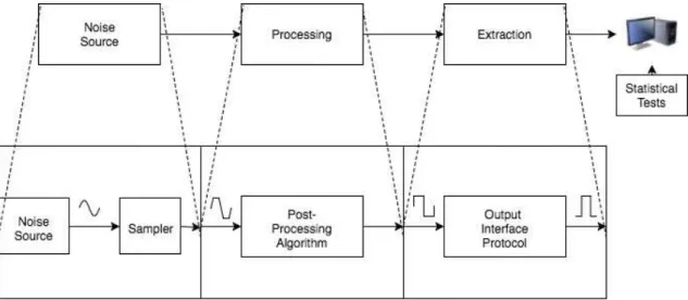
2.2 Basic RNG Architecture
Architecture of generators can be varied but a simple chain is mainly used. It is not defined this way, but it was proved to be efficient and thats why it still stands. This chain
usually comprises 3 steps:
• a noise source,
• a post processing block,
2 . 2 . BA S I C R N G A R C H I T E C T U R E
• an extraction block.
The first one is composed by a set of components which creates high entropy in the system. This signal is usually analog and then is then passed to the processing unit at a sample rate, the Digitised Analog Signal (DAS) is processed and extracted to the system which required the random number.
Figure 2.3: RNG general Architecture
Figure2.3represents the general architecture of a typical RNG building block. The noise source can be created using sources described previously, the entropy is then sam-pled at a rate in order to obtain the DAS, this sampling rate should be enough to capture the entropy of the system the most efficient as possible, i.e. if the systems evolves really
slow, a high sampling rate would oversample the noise source and as so the post process-ing unit would have to process large sets of sequences only to produce a bit. The samplprocess-ing rate must be either the ideal for the system or limited by technology.
2.2.1 Noise Sources
As described, there are many noise sources available, each one with its advantages and disadvantages. And as said in section 2.1, one the most important properties on noise sources is entropy [32].
Based on that, here are some examples of noise sources available:
• Electronic noise;
• Shot Noise;
• Metastability;
• Jitter;
C H A P T E R 2 . S TAT E O F T H E A R T
Electronic noise can also be considered thermal noise or johnson noise, since high/low temperatures makes the electrons move at higher/slower speed in a conductive material then this change makes subtle variations in the voltage of different components, quantum
noise makes the most use of radioactive decay to its entropy source. Zenner and avalanche diodes can produce breakdown voltages, this creates random DC current fluctuations which is mostly known for shot noise. Lastly Metastability and jitter noise are considered the ideal digital noise on TRNG’s, the metastability derives from the gates setup and hold times while jitter noise appears when rising and fall times are irregular, although jitter can be deterministic and non deterministic, in the random process only non deterministic jitter noise is considered.
2.2.2 Sampling
While some systems may require complex blocks to sample data like ADC’s and equiva-lent. In TRNG’s usually only a D-type Flip Flop is used to capture the random entropy output. The clock on the Flip Flop is it’s sampling rate, just as described in section2.2, this sampling rate should not be too fast neither too slow. The output of this Flip Flop is now a DAS that can be processed if required.
2.2.3 Post-processing
Post-processing sometimes is required because the output is not random due to some bias effects. This post processing aims to unbias the output from the sampler, like the
oversampling example, if the output is oversampling entropy then the result is bias to ’1’ or bias to ’0’. Post-processing is used to remove that effect from the sequences.
In order to accomplish this, many correctors can be used such as Von Neumann Cor-rector, XOR corCor-rector, Resilient functions, etc. All of these correctors attempt to remove bias or deterministic bits in the random sequence.
2.2.4 Output interface
After all the previous processes done, the output can be observed in a oscilloscope and we would be amazed by the changing ’1’s to ’0’s and vice versa, but this does not give us output required or the random numbers to evaluate the string. We can output the oscilloscope captured signal to the computer and analyse that with MATLAB, join groups of 8 bits into 1 byte of data, post ward generate a HEX from that resultant number and apply that to generate our random numbers, but the aim of the project is not to create something to be difficultly analysed. The devices in which this system can be
implemented do not have the same capabilities of an oscilloscope neither something near of that is required to the manufacturer. Hence, an extraction method needs to be implemented to provide a user-friendly tool.
2 . 3 . P R E V I O U S R N G ’ S WO R K S
2.3 Previous RNG’s works
2.3.1 Noise Amplification RNG
Figure 2.4: Noise Amplification RNG Circuit Schematic
Figure2.4presents a circuit schematic of a RNG block based on noise amplification techniques. The noise source is usually composed by a passive resistor, followed by an amplifier and sampled by a comparator.
This is simplest way to create a random analog generator. A bit sequence is generated based on a thermal noise source, the resistor changes its properties due to variations in the environment creating small voltage fluctuations, even small changes in the environment will create small voltage variations, it is mostly known as thermal noise.
This noise is really weak, therefore, an amplifier is needed to raise the noise to a voltage we can work on. The result of the amplification in then compared with a threshold voltage to assess if the output should be high or low logic level. Although this type of RNG appears to have no disadvantages because of its simplicity but in fact with a more careful look, this approach takes a lot of space in a IC and consumes a lot of power.
One of the major disadvantage of this design is due to the fact that these circuits when implemented need to be protected from the changes that occur from external sources like a power supply and substrate signals. Not having this protection, attacking this generator becomes easier since thermal changes can conduct to predictability in the bitstream. Afterwards it still needs a post processing unit that it’s not represented in the figure. Since this design is presented as very simple, that shielding part comes as a major disadvantage because of the size it needs in order to be effective. Although this type of design it’s still
used in cryptographic systems, it’s losing way to new technologies were some things need to be implemented digitally [23] [10].
2.3.2 Three Stage Noise Amplification RNG
Figure2.5shows a block a diagram of the circuit proposed on [23].
C H A P T E R 2 . S TAT E O F T H E A R T
Figure 2.5: Noise Amplification RNG proposed by [23]
the Analog-to-digital converter (A/D) and limiter comprise the discrete-time chaos and finally the current controlled oscillator(CCO) and the sampler comprise the oscillator sampling. This RNG works by joining all of the strengths from each of the RNG tech-niques. The low power noise is amplified and the discrete-time chaos block measures the phase difference of this noise to create a current to drive the CCO, finally this CCO is
then sampled the result can then be post processed as most of the RNGs. The solution proposed was the one on Figure2.5. The A/D used was a single-stage (bitcell)[24] due to its simplicity and lack of a true high impedance node, a current mode S/H [29] and the CCO is a five-stage current-starved inverter architecture [40].
Circuit performance presents itself with good results but with a bigger size than most of the rest of the RNGs.
Table 2.1: Three Stage RNG Performance Table
Maximum speed for ’near-random’ behaviour 4.7MHz Typical I/O ratio 0.4996 Performance with substrate noise interference unaffected
Maximum power supply variation 1.8Vpp
Area 1.5mm2
Power dissipation at 1 MHz 3.9mW Supply voltage 3 V
One the disadvantages presented on the table2.1 stand for the frequency at the be-haviour is described as ’near-random’, which is at 4.7 MHz and since the power dissipation and the presented working range are always described at 1 MHz, this presents a lack of information. Furthermore the chip die area of 1.5mm2is considered as high area when compared to other RNG implementations.
2.3.3 SiN MOSFET Ph-RNG
Since the first problems of the RNGs are area on the circuit, the low noise signal and the fact that these generators will require thermal noise. This approach was designed to deliver a small IC and a high generation rate, which was one of the problems too, there always been some kind of trade offbetween IC size and generation rate.
2 . 3 . P R E V I O U S R N G ’ S WO R K S
Figure 2.6: SiN MOSFET RNG proposed by [20]
Figure2.6presents the circuit schematic of a SiN noise based RNG that comprises a electron rich SiN substrate in order to create large magnitudes of noise, since this rich base creates a lot of noise, a sophisticated amplifier is no longer needed. A simple amplifier has been used followed by a high pass filter (HPF) designed to cut offlow frequency signals
originated by other sources than the SiN source. Just like the others RNG’s a comparator and a post processing unit was used to deliver the output bitstream.
This type of implementation can be used in smart cards, due to its size. Using this type of RNG can complement the smart card by giving it a really secure system since they already have a CPU, random logic, RAM, etc.. The results are good and it shows a really small circuit footprint, and much faster output results than previous works [20].
Conventional analog thermal noise generators , usually comprise a weak source fol-lowed then by an amplifier, filter, comparator and a post-processing block. This was and still is the standard of most RNG, this approach, since it already uses a high power noise, the size can be reduced in the amplifier and filter block. This provided a standard RNG in a much smaller area.
The performance of the block presented good results as well, variating from a large range of temperatures, the generation rate stays constant. Although this is presented as a small circuit, it does not have the lowest power consumption.
One of the disadvantages of this approach is the method for creating the SiN substrate, which requires specific methods in IC manufacturing. Other circuits proposed are bigger however even lower power than this one [2]. The design uses a SiN electron rich base which is temperature independent to generate a high noise signal.
2.3.4 Linear Feedback Shift Register RNG
A linear-feedback-shift-register (LFSR) is a basically a simple shift register in which the input bit is a linear function of its previous state. With a predisposed set of output bits all in an XOR gate, can develop the linear shift. The initial value of the LFSR is called the seed, and because the operation of the register is deterministic, the sequence of values produced by the register is completely determined by its current (or previous) state.
This is what is called a pseudo RNG because it only can draw a predisposed set of numbers.
Figure2.7shows anbit LFSR which comprisesnD-type flip-flops(FF) and an XOR gate.
This simple circuit works as sequence generator of 2n−1 different non-zero bit patterns
C H A P T E R 2 . S TAT E O F T H E A R T
Figure 2.7: LFSR RNGnbit
right and the output bit will be XORed with the bit that was previous in the n−thFF output. This random sequence can be obtained by give a predisposed set of bits to the flip-flops,X[i] inputs as a seed.
This implementation is as fast as technology can get the clock signal be generated. Some changes have been done to get more randomness out of this type of circuit, but most of them tried to get more longer cycles, meaning it would get more available patterns, still a Pseudo RNG but a lot harder to verify.
The main disadvantage on this type of implementation is its security. Since it is a PRNG, all of the results appear random but after a long cycle some patterns start to repeat. According to [27] this type of implementation produces sequences which are usable in a variety of applications like circuit testing, system simulation and Monte-Carlo method. All of them not needed for security but for analysis methods.
In Figure2.7we represent a simple LFSR RNG design, but such as Ring Oscillator RNG’s can be designed with multiple techniques, also LFSR’s present a lot of design techniques to obtain different results [5]. The more complex designs use mixed XOR
techniques, where more XOR gates are added. Those modifications also change pattern cycles but speed remains constant.
Figure 2.8: Tkacik LFSR CASR TRNG design
One of the TRNG implementations using LFSR’s is the Tkacik design. In this design the XOR sample 32 bits of a 43 bits LFSR and 32 bits of a 37 bit Cellular Automata Shift Register(CASR) [3]. These two blocks, CASR and the LFSR, were then sampled by two independent ring oscillators as a clock signal [34]. Although this design presents good qualities on the other hand as the designer shows, although it passed some random tests, the entropy source is limited to these two oscillators and similarly to the previous design
2 . 3 . P R E V I O U S R N G ’ S WO R K S
it uses a LFSR, the attacker could decrypt the model in order to predict its output. In [6] this design is criticised for its potencial weaknesses.
2.3.5 Ring oscillator RNG’s
One of the most reliable TRNG designs used are ring oscillators.
“A Ring oscillator is a cascaded combination of delay stages, connected in a closed loop chain. The ring oscillators designed with a chain of delay stages have created great interest because of their numerous useful features”[18]
Figure 2.9: Ring oscillator RNG design
Figure2.9shows a simple ring oscillator with 3 inverter gates.
This is composed by a odd number of delay stages(inverters) and a loop feedback to start all over, this creates a free running oscillation between high and low logic level.
The ring oscillator RNG design was first proposed by [32] and comprised several simple ring oscillators XORed and sampled by a simple D-type Flip-Flop. This simplistic design presented very good results and several other designs were attempted using this as a basis.
2.3.5.1 Ring oscillator TRNG design
The first design has been implemented in a FPGA and sampled at a frequency of 40 MHz. The ring oscillators had a fixed length of 13 inverters across 110 ROs. As post processing in this design resilient functions were developed. One of the major critics on this design are available in [6] and they rely on the statistical independence of the ROs on the original design. One characteristic of this design is the fact that the same RO but placed differently on the FPGA creates different entropy on the system.
One of the TRNG methods was proposed by [32] and it is represented by figure2.10. By having ’m’ ring oscillators composed of ’n’ NOT gates the analog output signal of the circuit can be found at the output of the binary XOR-tree to be sampled by the D-type flip flop.
C H A P T E R 2 . S TAT E O F T H E A R T
Figure 2.10: Ring oscillator TRNG design proposed by [32]
2.3.5.2 Ring oscillator Golic Figaro design
This design is also known as Fibonacci ring oscillator (FIRO).
It has the advantage of the LFSR inputs do generate entropy but with inverters to create even more entropy. According to its developers, it creates more entropy than normal ring oscillator with the same length of cascaded delays [6].
Figure 2.11: FIRO design
Like the LFSR, theFn values can be always changing in order to obtain higher
en-tropies. This ring design work similarly like the LFSR but they operate asynchronously so, apparently the design have the properties to present random behaviour. The other hybrid ring that derived from this implementation is the Galois ring oscillator design (GARO)
Figure 2.12: GARO design
The proposed from [6] is to create a regular design merging both designs. Results presented by the developers passed the proposed tests and seem to present good results. Although according to developer data, at each restart the behaviour does not appear to be random, randomness only appears after around, 40 ns.
2 . 3 . P R E V I O U S R N G ’ S WO R K S
2.3.5.3 Metastable RO TRNG
This design based on [35] exploits one of the most important properties on the ring oscillators: the metastability.
Every circuit component has this physical phenomenon, when it is excited with a fixed threshold voltage, it enters in a metastable state, a dynamical system state which is basically composed of noise and uncertainty around the desired value that is expected for the component to have. This uncertainty is again entropy, so this RO can create entropy. Metastability in this ring oscillator design occurs when a inverter gate is connected to its ouput and the voltage stochastically fluctuates around the value of the desired state.
Figure 2.13: Metastability RO
Figure 2.13 presents the design of the ring, which comprises a Multiplexer and a inverter gate per ring stage to create the metastability effect, also a clock generator and a
delay stage to capture the output of the RO. The testing was done using Cadence as well as an FPGA implementation. Tests to this RO topology proved that it performed well and that using a 65 nm technology, the total size of the ring was 1µm2.
2.3.5.4 Yang MultiMode TRNG
While most of the ROs produce high frequencies and create high jitter noise, there is one RO where this can be done with no additional inverters.
Figure 2.14: 3-edge RO proposed by [42]
C H A P T E R 2 . S TAT E O F T H E A R T
Figure 2.14 presents a ring proposed by [42] which is composed by inverters and NAND gates.
This ring works by injecting a signal between the RO, this way, if a certain ring oscillator produce 10 MHz oscillation the same RO using this design can produce 30 MHz oscillation with the same amount of logic gates. Although this seems quite simple to implement, another issue is that, this RO may suffer from injection locking and collapse
of the frequency injected, since not every single inverter gives the same delay, when a injection occurs, the frequency stays 3x higher than the nominal frequency until the first injection catches the second and then the third, and finally returning to the nominal frequency. The developer also has proved that longer rings tend longer to collapse while shorter rings collapse a lot faster.
This is how the RO proposed by [42] produces strong cumulative jitter which can also be seen as entropy. This RO design was not XORed with multiples ones but a different
approach was made. The TRNG uses one ring and measures the number of cycles in the RO until the collapse of the frequency. Then the process restarts to obtain a new number. This design has some weaknesses in the measurements of this collapses but the results shown are good and passed the proposed tests.
Ring oscillator RNG implementations present good results for the area used, and they do not consume a lot of power.
2.3.6 Arbiter physical unclonable function
One way to develop RNG is by the arbiter method. This method generates two signals with different timings and delays travelling on a series of components with different
char-acteristics, in the end where both arrive the ’arbiter’ chooses who came first. Therefore the ’arbiter’ is just a circuit that outputs the first signal to arrive. Since the way travelled by the signals is always different because of the different timings through the way, the
arrive order is always different.
Figure 2.15: Delay implementation for Arbiter PUF’s
2 . 3 . P R E V I O U S R N G ’ S WO R K S
Figure2.15presents a block diagram of a simple ’Arbiter’ physical unclonable func-tion (PUF), it complies the requirements, since it comprises a series of delays using mul-tiplexers followed by an ’Arbiter’ block at the end. The Mulmul-tiplexers work as switching boxes where the inputX[i] controls the signal switching from top/bottom. This way the signals race with each other and finally the latch decides who got first. This type of cir-cuit is the basic concept of the arbiter PUF, but can be ’hacked’ if someone knows all the timings involved. Therefore, other type of techniques needed to be studied and pursued in order to get more secure systems. One of them is to obfuscate the signals output with an XOR.
In terms of performance, since it only relies on delay times, it is very robust against environmental variations.
“For realistic changes in temperature from 20◦ to 70◦ Celsius and regulated voltage changes of ±2% , the output noise is 4.8% and 3.7%, respectively. Even when increasing the temperature by 100◦C and varying the voltage by 33%, the PUF output noise still remains below 9%.”[31]
This type of circuit can become a lot more complex in order to become more secure, higher output rates or even more randomness.
Figure 2.16: Arbiter PUF with Oscillators [31]
In section2.3.5we reviewed RO, they can also be implemented alongside with an ’Arbiter’ PUF. Figure 2.16 shows a ring oscillator PUF implementation. It uses some concepts based on ROs and other based on the arbiter delay system. It is composed by several ROs in parallel to generate a signal and all of them joined together using two Multiplexers. Since all of the separate ROs oscillate at a different frequency, this creates
C H A P T E R 2 . S TAT E O F T H E A R T
it is much slower than the previous arbiter implementation. The slower output rate is the only disadvantage when compared with the ’arbiter’ PUF, since it can also give more ’random’ sequences.
Since this design is completely digital, it can be implemented using an FPGA which will give some sort of freedom when designing the circuit. This presents another major advantage over the other designs previously referred.
C
h
a
p
t
e
r
3
T R N G d e s i g n
After evaluating the prior work done and the state-of-the-art, it has been decided that the best implementation of the noise source should be based on ring oscillators.
All the experiments and designs are described in this chapter.
3.1 Hardware
Our design has been made using Xilinx ISE version 14.7 (nt64) and was mainly developed in VHDL. Xilinx platform provides an excellent environment to develop code and digital circuits for FPGA. The platform was created to code, syntethise, translate, map, place and route and finally implement the design on the desired FPGA. Basically, there is no need to interact with other platforms to implement designs. No simulations were made using the simulator incorporated in the platform due to timing restrictions and logic impossibilities.
3.1.1 Spartan 3 FPGA board UG130
Alongside with the Xilinx software, the project has been implemented in a Spartan 3 starter Kit UG130 FPGA with a X3S200FT256 device. Spartan 3 Family boards are well known for its precision, this specific board is known to be the best starter kit in FPGA systems development.
Many cloud based servers do have FPGA available as hardware security modules as well as some IoT devices which possess small FPGA to implement hardware functions. Therefore, they are the perfect way to prototype our RNG.
Some key features presented on this board are:
C H A P T E R 3 . T R N G D E S I G N
• Twelve 18K-bit block RAMs (216K bits)
• Four Digital Clock Managers (DCMs)
• Up to 173 user-defined I/O signals
• 2 Mbit Xilinx XCF02S Platform Flash, in-system programmable configuration PROM
• 3-bit, 8-color VGA display port
• 9-pin RS-232 Serial Port
• 50 MHz crystal oscillator clock source
• JTAG port [30]. . .
3.1.2 Oscilloscope
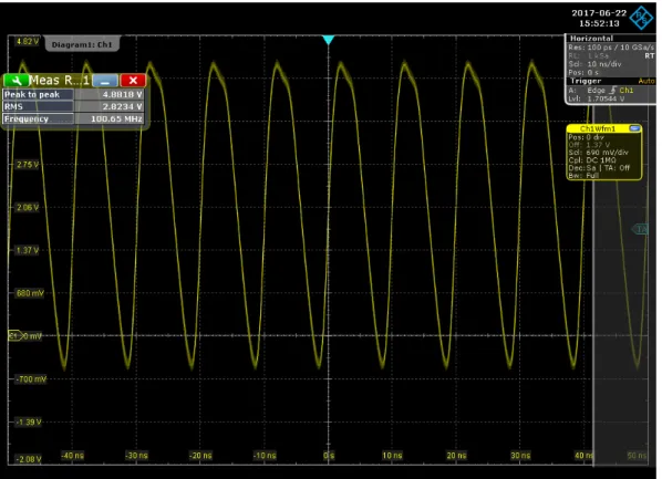
All the measurements and signal testing were carried out using a Rhode & Schwartz RTO1022 Digital Oscilloscope. Some key features that worth mentioning are the 2 GHz bandwidth, 10 GSamples/s for 2 channels and a digital record rate for up to 40 M samples. The analog signal was read using a RT-ZP10 passive probe.
3.2 Cryptography using FPGA’s
For quite some time FPGA are used to create cryptographic systems [41], as it is referred in section 3.1.1, one of the reasons FPGA are still in use rely on the fact that many systems require flexibility. Some systems require to be restructured without the need to physically replace all integrated circuits (ICs). FPGA’s provide that advantage to users. In Cryptography, all the work can be done using software, but although that approach worked in the past, in recent years, that approach needed to change.
Our project aims to develop a new TRNG design using an FPGA for prototyping and for proof-of-concept. The final project can later be ported to an application specific integrated circuit (ASIC) or simply just ported to a different FPGA family device and
implemented in the target device as a firmware.
An FPGA consists of a series Configurable Logic Blocks (CLBs), Input/Output pads (I/O) and routing channels connecting all of them together. These CLB’s have flip-flops and lookup tables (LUT’s) to implement the systems designed by the user. The netlist is implemented by the lookup tables and flip flops, multipliers, blocks of RAM, several IP cores and in the more recent FPGA boards, we have processor cores too in order to have a full SOC. Basically, the FPGA is a platform that allows the user to create digital circuits in a flexible and straight forward implementation. The design is coded in VHDL or via SCH on the ISE and then the same ISE reads that code and optimises that design into the target FPGA.
3 . 3 . R I N G O S C I L L ATO R T R N G D E S I G N
Table 3.1: XOR Truth Table
A B A XOR B
0 0 0
0 1 1
1 0 1
1 1 0
Table 3.2: XOR Multi input Truth Table
Input Output Odd number of 1’s 1 Even number of 1’s 0
3.3 Ring oscillator TRNG design
The starting point for this project was as a first step to implement a ring oscillator RNG based on an XOR TRNG design [32], while attempting to improve performance and reducing the FPGA usage.
As described in section 2.3.5, ring oscillators (ROs) are composed by a cascade of inverter gates in a odd number with the last inverter output looped back to the input of the first inverter, acting as a feedback net. This creates a continuous oscillating sequence between high and low logic value.
Figure2.9shows the simplest approach to implement a RO, composing 3 NOT gates (inverter gates) connected in a feedback loop. This simple design is very susceptible to jitter noise which stands as a valuable property to increase entropy as a noise source.
To implement this as an RNG, several rings are XORed together and sampled by a D-type flip-flop at a frequency Fs, which will capture the jitter existent in the rings
[32][29]. Since XOR is a special function represented by table3.1and mostly represented by exclusive OR, or EXOR, this function outputs ’0’ when signals are equal, and ’1’ when different. When there is more than two inputs on the gate, the output is as described in
table3.2. This data can be found on Xilinx ISE Help.
According to [2] for a better result, it is advised that several rings of different lengths
should be used instead of a many rings with the same length.
3.4 Ring design and properties
C H A P T E R 3 . T R N G D E S I G N
synthesised if there is no input to the ring, figure3.1presents a solution to that problem. The first inverter gate was replaced with a NAND gate, in which one of the inputs is the enable signal that triggers the ring oscillation process.
Figure 3.1: Ring oscillator with enable signal
Another problem that Xilinx presents to the developers, is due to the fact that several rings with the same length, XORed together and again, timings apart, they were all be the same if there were no jitter noise or different timings. The hierarchy on the synthethiser
did not removed this issue, so the solution was to create a property on every net with the parameter KEEP set to TRUE, allowing it to not remove the oscillators.
Issues apart, several configurations and properties where explored and tested in order to prove some concepts.
3.4.1 Rings’ length
The length of each RO was the first property tested when developing this system. Some conclusions were already been made on previous works regarding ROs’ length [33].
According to [18], the resultant frequency of the oscillator depends on the propagation delay,τd, per inverter stage, meaning that the length of the ring directly affects the output
frequency. Therefore,
fo=
1 2mτd
where the factor of delay,τd, depends on many non linear variables and parasitics on the
circuit. In order to test the properties on ’long’ and ’short’ ROs, two ring oscillators were designed and implemented. The two lengths used was 7 and 101 for short and long ROs, respectively.
3 . 4 . R I N G D E S I G N A N D P R O P E R T I E S
Figure 3.2: Ring oscillator 7 inverters
Figures3.2and3.3represent the output of the two ROs and the first thing that can be observed is the frequency associated with the oscillation. As expected, the longer RO presented a lower frequencies when compared to shorter one. As seen in previous figures, the RO with 7 inverter stages presented a frequency around 100MHz and the one with 101 inverters has only 7MHz. Applying the previous equation,
τd≈0.7ns
Considering this value, is possible to estimate roughly the frequency of the oscillation, but just as described in this section, many factors can influence it.
In the next section will be discussed another property which can influence these values.
3.4.2 Placement of the rings
Since Xilinx offers many tools to manually place components as well as many other
op-tions to optimise the design placing on the FPGA Floor. We attempted to place the same RO on multiple sites in order to test the increase of uncertainty, reads entropy. Figure
3.2shows the waveform resultant of a simple RO design with 7 inverters using the auto placement tool available on Xilinx for maximum delay.
C H A P T E R 3 . T R N G D E S I G N
Figure 3.3: Ring oscillator 101 inverters
Figure 3.4: Manual placement test for higher delay
Figure3.4represents a test placement to achieve a higher delay on a RO. The first, third and fifth inverter gate where put in pblock1 while the rest was set on pblock2, this placement achieves a higher traveling path for the signals to run.
Figure3.5represents the output of the experiment. As can be seen this was proved
3 . 4 . R I N G D E S I G N A N D P R O P E R T I E S
Figure 3.5: Ring oscillator with 7 inverters in a specific placement for maximum delay
to be correct, since the previous RO design with the same amount of stages presented an output of around 100 MHz and this one was reduced to about 27 MHz and a different
waveform output. Applying the same equation, we obtained
τd ≈2,64ns
Hence, a specific placement will increase propagation delay as expected in a significant way.
Figure 3.6: RO with 101 inverters manual placement
C H A P T E R 3 . T R N G D E S I G N
with 101 inverter gates, again with the same placement as3.4. And again the frequency decreased from 7 MHz to 2.5 MHz. The propagation delay,
τd≈1.9ns
which stands for a significant change from the previous test. Another conclusion from these tests was cycle-to-cycle jitter which will be discussed in the next section, again as a property that can be used to further increase entropy.
3.4.3 Jitter and Phase noise analysis
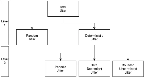
Jitter uncertainty (noise) can be considered as an undesired property on most of our electronics due to its uncertainty on the signals time domain. It can be categorised as represented in Figure3.7.
Figure 3.7: Jitter noise classification
It is considered as deviation from the expected time where the signal was supposed to happen, and since it is a deviation most electronics work based on perfection and small deviations affect performance a lot [22].
Random Jitter is the type of jitter we are looking for in our project, since it is consid-ered non deterministic. Normally it is also called gaussian jitter because usually it follows a normal distribution but also stands as an unpredictable electronic timing noise [1].
Jitter on signals can be measured in three main ways:
• Period jitter,
• Cycle-to-cycle jitter,
• Time interval error jitter,
3 . 4 . R I N G D E S I G N A N D P R O P E R T I E S
The first one attempts to measure the time deviation on each period, while the last one measures the deviation from the reference point of the ideal signal.
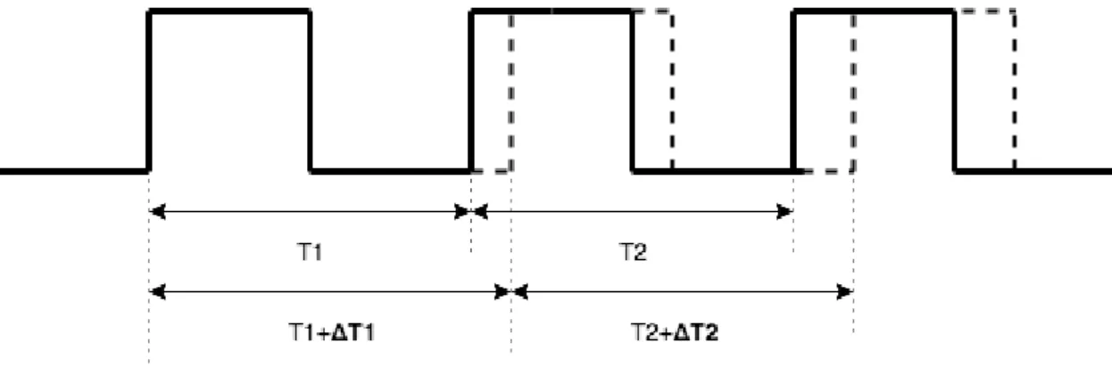
Cycle-to-cycle jitter (CCJ) is the measurement that applies to our calculations [18], since it will measure the differences in the period between adjacent cycles which are more
meaningful for free running oscillators while others apply for example in PLL oscillators. Figure3.8illustrates this calculation and graphic representation of this measurement.
Figure 3.8: Cycle-to-cycle jitter
Cycle-to-cycle jitter is calculated by,
CCJ=∆T2−∆T1
When this happens in real time for the infinite number of samples,
∆T
cc= lim N→∞ v u t 1 N N X n=1
(Tn+1−Tn)2
Phase noise also characterises the same noisy process, but this time using the power spectral density. It is estimated as [12] [15],
L(fof f) =
Psid
fo+fof f,1Hz
Pcarrier
withPsidas the single sideband power at the frequency offsetfof f from the carrier in the
1 Hz bandwidth, andPcarrier being the power of the carrier as represented in figure3.9.
The units of this representation is Decibel below the carrier per hertz (dBc).
C H A P T E R 3 . T R N G D E S I G N
Figure 3.9: Phase noise per unit bandwidth
Figure 3.10: Jitter wizard on manual placed design with 7 delay stages
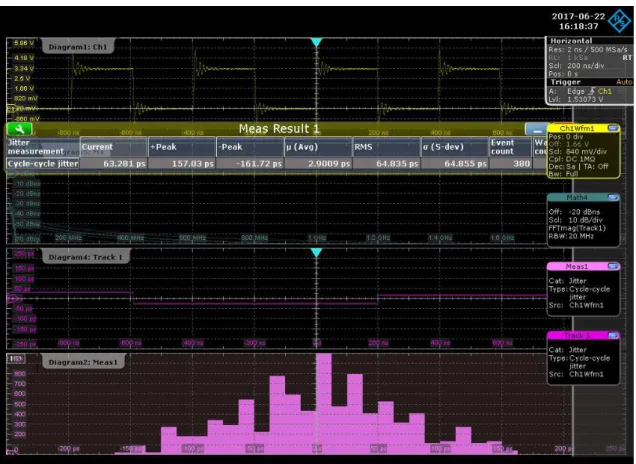
3 . 4 . R I N G D E S I G N A N D P R O P E R T I E S
Figure 3.11: Jitter wizard on auto placed design with 7 delay stages
Figure 3.10 and3.11 represents this comparison and as can be seen the standard deviation, σ, is about 13.6 psin the auto placed design and about 60ps in the manual placed. This means that the manual placed design accumulates more jitter as expected, due to the longer signal travelling path. The longer path will introduce more resistance on the signals which can be translated as an higher number of external variables affecting
C H A P T E R 3 . T R N G D E S I G N
Figure 3.12: Jitter wizard on manual placed design with 101 delay stages
The placed design presented a standard deviation of around 65ps, as the non placed presented around 53 ps as figure3.12 and3.13 represents. It would be expected that the placed design presented a higher CCJ but as this happens in the shorter RO, the same does not happen on the longer one. The conclusion on this test is that shorter ROs, accumulate more jitter when placed and longer rings present the same high jitter even when they are not manually placed, meaning that the manual placement to increase jitter does not worth the increase in die area/size, in contrast, shorter rings do worth it.
3.4.4 Ring oscillator topology
The RO topology to implement on the XORed method was the Multimode ring oscillator [42].
Just as presented in chapter 2, this design is based on a multi injection RO which can improve the jitter accumulation and oscillate at much asmtimes the number of injections on the RO when compared to the same amount of gates. Although this design has been used to a create a TRNG with a different method, our project will attempt to create a
XOR ring oscillator TRNG [32] with multimode ring oscillators [42]. This design for not being as simple as the first approach, provided a problem According to the developer, each RO tend to collapse to its nominal frequency, which is the frequency at which the
3 . 4 . R I N G D E S I G N A N D P R O P E R T I E S
Figure 3.13: Jitter wizard on auto placed design with 101 delay stages
same amount of inverter gates on a ring would oscillate, this happens when the multi injections get caught on each other.
Figure3.14presents the output of two ring oscillators with 9 cascaded inverters, as can be seen the two outputs are oscillating at almost the same frequency, which means that the multimode implementation already as collapsed to its nominal frequency. A solution was then required to take advantage of the RO topology.
C H A P T E R 3 . T R N G D E S I G N
Figure 3.14: Ring oscillators with 9 inverter gates proposed by [42] and [32]
Figure 3.15: Ring placement on far apart and close interaction
3 . 5 . E N T R O P Y S O U R C E A N D SA M P L E R
a Test ROs close to each other b Test ROs far apart
Figure 3.16: Waveform comparison between RO spacing
Figure 3.16 which represents the output waveforms associated with the two tests, the only influence present on the result was a specific harmonic which derived from the injection locking of the two RO since they are really close to each other, the same was concluded on jitter wizard [25].
One of the main conclusions from this test was that as long as there is a small prohib-ited gap between the rings, not much influence would be sensed.
3.5 Entropy source and sampler
The entropy source of the proposed RNG is composed by different length multimode ring
oscillators all XORed together [32][42] as described earlier on this document. These rings presented a challenge when it comes to maintaining its properties. Hence, an auto reset block was designed.
The entropy source was designed with rings having lengths 9,13,15 and 21 with man-ual placement in order to increase the jitter on each RO.
Figure3.17represents the final entropy block diagram, which is comprises 9 RO for each ring’ length, XORed and sampled by a D-type flip-flop at 50 MHz and having all the rings restarted with a pulse slow enough to prevent the rings from collapse. Tests shown that anything below 500 kHz worked, but ended up being in 25 kHz for best performance on our design.
C H A P T E R 3 . T R N G D E S I G N
Figure 3.17: Final entropy source block and sampler
Figure 3.18: Pulse generator
As seen in sections3.4.2and3.4.1, with manual placement and ring’ length tests, the ROs used have a length of 9, 13, 15 and 21, these lengths do not represent nothing in particular.
According to previous conclusions, the shorter rings which oscillate at a higher fre-quency were placed to achieve a higher signal traveling path, and the two longer ROs were put to auto placing in a specific region of the FPGA floor. This placement has been achieved having the maximum possible jitter in mind.
Figure3.19represents the final placement scheme of the ROs on the FPGA floor. The RO with length 9 has been split in groups of 3 inverters, having the first group been placed on pblock1, the second on pblock3 and the third on pblock2. On ROs with length 13, have been also split in groups of 3 inverters having the first, the third group and the last inverter on pblock5 and the rest on pblock4. Finally the ROS with length 15 have been auto placed on pblock7 and ROs with length 21 on pblock6.
The reddish areas are defined a prohibited areas for the Synthesiser.
3 . 5 . E N T R O P Y S O U R C E A N D SA M P L E R
Figure 3.19: Final ROs placement
3.5.1 ROs data analysis
All the ROs with the same length have been XORed together and the ouput has been recorded using the oscilloscope and processed in Matlab. One of the basic signal analysis that can be made on the output of the rings is the Fast Fourier Transform(FFT). The FFT is a signal processing method that allows us to obtain the harmonic frequencies that compose a signal.
Figure3.20represents the signal on time domain as well as the corresponding FFT on the frequency domain. We can conclude that most of the signals oscillate at around 60 to 80 MHz and not having notably valued harmonics expect on RO with a length of 15 inverters presenting many harmonics. The same analysis has been carried out with the outputs of all the XORed ROs with lengths of 9 and 13.
C H A P T E R 3 . T R N G D E S I G N
Figure 3.20: FFT of the RO output
Figure 3.21: FFT of the XOR RO output
Also, in the same figure and highlighted, we can see a zone of the spectrum where there is a slight influence from the ROs, this presents no problem because all the outputs from all of the different ROs will be XORed and these frequencies will be masked as
expected. Figure3.22shows that no frequency components can be found on the output from all the ROs.
In addition to the FFT analysis, an Autocorrelation test was also carried out. Again, this analysis has been done using Matlab.
Autocorrelation and crosscorrelation are two properties that attempt to measure the
3 . 5 . E N T R O P Y S O U R C E A N D SA M P L E R
Figure 3.22: FFT of the Entropy source output
degree of similarity between two signals, whereas, the crosscorrelation measures the similarity between two signals and the autocorrelation is the same as a crosscorrelation of the signal with himself, which can be represented the following equation,
f ⋆ f =
Z ∞
−∞
f (u+τ)f (u)du
Figure 3.23: Graphical representation of the autocorrelation
Figure3.23represents the graphical representation of the same equation.
Furthermore, we carried out this in Matlab and we performed an autocorrelation on the signals from the XOR output of ROs with length of 9 and 13.
C H A P T E R 3 . T R N G D E S I G N
a Signals representation b Autocorrelation graphic results
Figure 3.24: Autocorrelation on XOR output of two ROs of different lengths
3.5.2 Jitter analysis on multimode ring oscillators
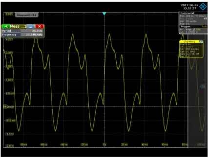
To analyse the jitter of the ROs, again has been used the jitter wizard of the oscilloscope, which proved to be a very useful tool on the development of the TRNG.
3 . 5 . E N T R O P Y S O U R C E A N D SA M P L E R
C H A P T E R 3 . T R N G D E S I G N
Figure 3.26: Jitter analysis on the length 13 Multimode Ring
3 . 5 . E N T R O P Y S O U R C E A N D SA M P L E R
![Figure 2.14 presents a ring proposed by [42] which is composed by inverters and NAND gates.](https://thumb-eu.123doks.com/thumbv2/123dok_br/16583337.738659/44.892.143.763.886.1112/figure-presents-ring-proposed-composed-inverters-nand-gates.webp)