Ricardo Vaz Moreira
Reconfigurable hardware for the
new generation IoT video-cards
Novembro de 2019
Ricardo Vaz Moreira
Reconfigurable hardware for the
new generation IoT video-cards
Dissertação de Mestrado em Engenharia Eletrónica
Industrial e Computadores
Trabalho efetuado sob a orientação do
Professor Doutor Sandro Pinto
Novembro de 2019
DIREITOS DE AUTOR E CONDIÇÕES DE UTILIZAÇÃO DO TRABALHO POR TERCEIROS
Este é um trabalho académico que pode ser utilizado por terceiros desde que respeitadas as regras e boas práticas internacionalmente aceites, no que concerne aos direitos de autor e direitos conexos.
Assim, o presente trabalho pode ser utilizado nos termos previstos na licença abaixo indicada. Caso o utilizador necessite de permissão para poder fazer um uso do trabalho em condições não previstas no licenciamento indicado, deverá contactar o autor, através do RepositóriUM da Universidade do Minho.
Atribuição-NãoComercial-CompartilhaIgual CC BY-NC-SA
Aos meus pais, Almeno Moreira e Maria da Luz Vaz, dedico as minhas primeiras palavras de agradecimento, por todo o apoio dado, não só ao longo desta dissertação, mas ao longo de todo o meu percurso académico.
À minha irmã, Mónica Moreira, dedico este segundo parágrafo, pelo suporte e amizade que, apesar de nem sempre serem evidentes, está intrínseco na nossa relação.
Ao meu orientador, Sandro Pinto, que com o seu conhecimento, experiência e espírito de liderança soube bem definir o caminho a ser seguido. Um exemplo a seguir.
Ao meu co-orientador, Mestre e futuro PhD Miguel Costa, pela transmissão de conhecimento, perfecionismo e rigor que foram essenciais para concluir este trabalho.
Aos meus amigos de curso, em especial ao grupo ”ESRG Top Students”, por todo o apoio, amizade e momentos de felicidade partilhados ao longo do meu percurso académico.
A todos os meus professores que durante estes longos anos me transmitiram conhecimento. À minha restante família e e amigos que me ajudaram ao longo do meu percurso académico: o meu sincero Obrigado!
I hereby declare having conducted this academic work with integrity. I confirm that I have not used plagiarism or any form of undue use of information or falsification of results along the process leading to its elaboration.
I further declare that I have fully acknowledged the Code of Ethical Conduct of the University of Minho.
Reconfigurable hardware for the new generation IoT video-cards
Embedded systems became a crucial research and developing area because of the dependence of society on devices and the growing demand for new technology products in our lives. The video industry is an example of remarkable technological advances by exploiting the hardware performance for bringing new video products along with even better video quality and higher resolution. Today is time for Ultra High Definition (UHD) resolution and the next new feature is the 8k. A relevant area that may benefit from 8k is medicine, by improving the detail and image quality in diagnoses. Moreover, Japan is preparing to become the first 8k transmitter at the 2020 Olympics.
In spite of existing already general-purpose solutions for managing efficiently UHD video, the deployment of a customized configurable solution can be useful for a specific system needs. Besides, it may dictate market favorable positioning on meeting new market demands by providing faster upgrades. For addressing this problem, this MSc thesis proposes a hardware-based deployment of two essential reconfigurable cores for a new generation IoT UHD Video-Card, for managing huge memory accesses as well as for compressing video. The memory management provides a memory direct access for dealing with variable video resolution up to 8k, as well as data error control, frame alignment, configurable memory region, and more. The video compression is performed by a configurable core based on an open-source H.264 encoder. The results presented show it was achieved 8k real-time video streaming along with extra control and status functionalities. Video encoding was achieved for up to 8k.
Keywords: 8k, FPGA, H.264, video.
Reconfigurable hardware for the new generation IoT video-cards
Os sistemas embebidos tornaram-se uma área fulcral de pesquisa e desenvolvimento devido à dependência da sociedade em dispositivos e à crescente procura por novidades tecnológicas para o quotidiano. A indústria de vídeo é um exemplo do notável avanço tecnológico ao explorar o desempenho máximo do hardware para trazer maior qualidade de vídeo e maior resolução. A resolução de vídeo UHD já é uma realidade e a próxima novidade é o 8k. Uma área de relevo que pode beneficiar do 8k é a medicina, com maior detalhe e qualidade de imagem em diagnósticos. Além disso, o Japão está preparar-se para se tornar o primeiro transmissor de 8k nas Olimpíadas de 2020.
Apesar de existirem soluções capazes de gerir com eficiência vídeo UHD, uma solução personalizada e configurável pode ser útil para as necessidades específicas de um sistema. Além disso, pode ditar um posicionamento dianteiro no mercado ao atender às novas exigências do mercado fornecendo novidades mais rapidamente.
Como possível solução para os problemas expostos, esta tese propõe o desenvolvimento de dois núcleos de hardware reconfigurável essenciais para uma nova geração de placas IoT de vídeo UHD, para gerir acessos à memória assim como para compactar vídeo. A gestão de memória desenvolvida fornece acesso direto à memória para lidar com resolução de vídeo variável e até 8k, além de controlo de erros de dados, alinhamento de frames, região de memória configurável e muito mais. A compactação de vídeo é realizada por um núcleo de hardware configurável, baseado num Encoder H.264 de código aberto. Os resultados mostram que foi alcançada transmissão de vídeo 8k em tempo real, além de funcionalidades extras de controlo e estado. A codificação de vídeo até 8k foi alcançada.
Palavras-chave: 8k, FPGA, H.264, video.
1 Introduction 1
1.1 Problem Statement . . . 1
1.2 Aim and Scope . . . 2
1.3 Document Structure . . . 3
2 State of the Art 4 2.1 Background . . . 4
2.1.1 Serial Digital Interface . . . 4
2.1.2 Memory Management . . . 7
2.1.3 H.264 Encoding . . . 10
2.1.4 Peripheral Component Interconnect Express . . . 16
2.2 Related Work . . . 16
2.2.1 UHD Demosaicing on Low-Cost FPGA Pavel . . . 17
2.2.2 AJA Kona IP . . . 17
2.2.3 DELTA-3G-elp-tico-d 4C . . . 18
2.2.4 Magewell Pro Capture AIO 4K Plus . . . 18
2.2.5 Bluefish444 Kronos Optikos . . . 18
2.2.6 Dektec DTA-2179 . . . 19
2.2.7 Discussion . . . 20
3 System Specification 21 3.1 Development Environment . . . 21
3.1.1 Zynq UltraScale+ MPSoC ZCU102 . . . 21
3.1.2 AMBA Advanced eXtensible Interface . . . 25
3.3 Memory Manager and H.264 Encoder Dataflow Overview . . . 33 3.4 Memory Manager . . . 34 3.4.1 Configuration Subsystem . . . 37 3.4.2 Write Subsystem . . . 41 3.4.3 Read Subsystem . . . 45 3.5 H.264 Encoder . . . 47 3.5.1 Configuration Subsystem . . . 51
3.5.2 Data Acquisition Subsystem . . . 53
3.5.3 Data Transmission Subsystem . . . 55
4 System Development 57 4.1 Memory Manager . . . 57 4.1.1 Configuration Subsystem . . . 58 4.1.2 Write Subsystem . . . 60 4.1.3 Read Subsystem . . . 64 4.2 H.264 Encoder . . . 67
5 Evaluation and Results 73 5.1 Memory Manager Core Functionalities . . . 74
5.1.1 Double Buffering mechanism . . . 74
5.1.2 Memory Rotation . . . 75
5.1.3 Frame Error Detection Mechanisms . . . 76
5.1.4 Frame start address rectification . . . 77
5.1.5 Data loss detection . . . 78
5.2 H.264 Encoder Core Functionalities . . . 78
5.2.1 Working time in encoding . . . 78
5.2.2 Buffers Addressing Algorithm . . . 79
5.3 Hardware Costs . . . 80
5.4 Conclusion . . . 81
A Appendix 87
Bibliography 90
2.1 Required bit rate to transmit various video formats [1]. . . 6
2.2 Advanced Extensible Interface (AXI) Video Direct Memory Access (VDMA) Block Diagram (Adapted from [2]). . . 9
2.3 Intra-prediction modes for 4x4 Macroblock (MB)[3]. . . 13
2.4 Example of Multi Reference Motion Estimation. . . 14
2.5 H.264 Bitstream Structure. . . 15
2.6 AJA Kona IP [4]. . . 17
2.7 Delta-3G-elp-tico-d 4C [5]. . . 18
2.8 Pro Capture AIO 4K Plus [6]. . . 18
2.9 Bluefish444 Kronos Optikos [7]. . . 19
2.10 Dektec DTA-2179 [8]. . . 19
3.1 Zynq UltraScale+ MPSoC Overview Block Diagram [9]. . . 22
3.2 Zynq UltraScale+ MPSoC Processing System (PS) and Programmable Logic (PL) Block Diagram [9]. . . 23
3.3 Timing diagram for AXI4-Memory Mapped read and write operations. . . 25
3.4 AXI4 Read channel timing diagram [10]. . . 26
3.5 AXI4 Write channel timing diagram [10]. . . 27
3.6 Hardware Description Language (HDL) General Architecture of the Reconfigurable Video-Card. . . 31
3.7 Dataflow of the Memory Manager and H.264 Encoder. . . 34
3.8 Stream with four pixels structured in V210 format. . . 35
3.9 Stream with four pixels structured in YUYV format. . . 35
3.10 Memory Manager Intellectual Property (IP) core General Architecture. . . 37 xii
being saved in memory. . . 43
3.13 Example of buffer rotation when the configured address is not aligned to fill an entire frame YUV 4:2:2 640×480. . . 44
3.14 Read subsystem of Memory Manager Main state machine. . . 46
3.15 Mechanism to count the frames not streamed from memory. . . 46
3.16 H.264 Encoder input and output signals. . . 47
3.17 H.264 Encoder - Main state machine. . . 49
3.18 H.264 Encoder interface Y color component State Machine. . . 50
3.19 H.264 Encoder interface UV color component State Machine. . . 51
3.20 H.264 Encoder algorithm scheme to determine a equation for addressing Y/UV buffers. Example for 64x16 frame resolution. . . 53
3.21 H.264 Encoder header delivering State Machine. . . 56
5.1 Double-buffering mechanism test - Integrated Logic Analyzer (ILA). . . 75
5.2 Memory rotation test - ILA. . . 76
5.3 Early end of line error test - ILA. . . 76
5.4 Late end of line error test - ILA. . . 77
5.5 Start of frame error test - ILA. . . 77
5.6 Frame start address rectification test - ILA. . . 77
5.7 Data loss detection test -ILA. . . 78
5.8 Working time for the H.264 Encoder - ILA. . . 79
5.9 Buffers addressing algorithm - ILA. . . 79
5.10 Field Programmable Gate Array (FPGA) Resources - Memory Manager vs VDMA. . . 81
A.1 8k frame written and read by Memory Manager. . . 87
A.2 8k encoded frame in format H.264 failed. . . 88
A.3 4k encoded frame in format H.264 succeeded. . . 88
2.1 AXI VDMA Features. . . 10
2.2 Exponential-Golomb code words. . . 15
2.3 Peripheral Component Interconnect Express (PCIe) bandwidth for different generations and lane configurations, based on [11] and [12]. . . 16
2.4 Characteristics summary of the analyzed Video-Cards. . . 20
3.1 Zynq UltraScale+ MPSoC ZCU102 Features and Resources [9]. . . 23
3.2 AXI4 Read address channel signals [13]. . . 26
3.3 AXI4 Read data channel signals [13]. . . 27
3.4 AXI4 Write address channel signals [13]. . . 28
3.5 AXI4 Write data channel signals [13]. . . 28
3.6 AXI4 Write response channel signals [13]. . . 29
3.7 AXI4-Stream channel signals [13]. . . 29
3.8 Memory Manager register address map. . . 38
3.9 Raw video control register of Memory Manager (00h Offset). . . 38
3.10 Raw video status register of Memory Manager (28h Offset). . . 40
3.11 Encoded video control register of Memory Manager (30h Offset). . . 41
3.12 Encoded video status register of Memory Manager (48h Offset). . . 41
3.13 H.264 Encoder register address map. . . 52
3.14 H.264 Encoder control register (0×00). . . 52
5.1 Resource utilization. . . 80
4.1 Error register update. . . 58
4.2 Pulse generation and bit clear by hardware. . . 59
4.3 Counter updating for tracking input and output data from buffers. . . 60
4.4 Next address updating in the top Module. . . 62
4.5 Next burst transaction updating Address register. . . 63
4.6 Reading start control in the Main Read State Machine. . . 64
4.7 Calculates the new frame address to keep frames in the expected addresses or to rotate memory. . . 65
4.8 Counter for frame width tracking, according to pre-configured parameters. . . 66
4.9 Combinational logic for AXI Stream Video Signals. . . 67
4.10 Updates the width counter and odd line for conversion from YUYV 4:2:2 to YUV 4:2:0. . 68
4.11 Reconfigurable input data and conversion from YUYV 4:2:2 10-bit to YUV 4:2:0 8-bit by combinational logic. . . 69
4.12 Algorithm for addressing Y MBs. . . 70
4.13 Algorithm determination of Exponential Golomb for frame width header coding in Encoder H.264 header. . . 70
4.14 H.264 Encoder header SPS. . . 72
5.1 Example Software Core configuration for Memory writting Rotation. . . 75
AMBA Advanced Microcontroller Bus Architecture. API Application Programming Interface.
ASI Asynchronous Serial Interface. AXI Advanced Extensible Interface. BME Block Motion Estimation. BNC Bayonet Neill–Concelman. BRAM Block RAM.
COTS Commercial-Off-The-Shelf. CPU Central Processing Unit. DDR Double Data Rate. DMA Direct Memory Access. FHD Full High Definition.
FPGA Field Programmable Gate Array. fps frames per second.
HDL Hardware Description Language. HDMI High Definition Multimedia Interface.
IDE Integrated Development Environment. ILA Integrated Logic Analyzer.
IoT Internet of Things. IP Intellectual Property. LUT Look Up Table. MB Macroblock.
MPSoC Multi Processor System on Chip. NAL Network Abstraction Layer.
PCIe Peripheral Component Interconnect Express. PL Programmable Logic.
PS Processing System. QP Quantization Parameter. RAM Random-Access Memory. RTL Register Transfer Level. SD Standard Definition. SDI Serial Digital Interface. SDK Software Development Kit. SFP Small Form-factor Pluggable.
SMPTE Society of Motion Picture and Television Engineers. SoC System on-Chip.
VDMA Video Direct Memory Access. VTPG Video Test Pattern Generator.
The present chapter outlines the problem addressed in this MSc thesis, as well as the goals that must be achieved in order to present a solution for solving that problem. Finally, a brief description of the structure of this document is presented.
1.1 Problem Statement
Due to the strong growth of the electronic industry and the demand for improved devices required for society, embedded systems have been facing even more challenging problems over the years. Currently, there is plenty of domains in which embedded system are applied, from basic consumer electronics [14], Internet of Things (IoT) devices [15, 16], aerospace control systems [17], medical devices, machinery [18, 19, 20], and more.
Over the years, we attended the improvement of image resolution. Now it is time for more and more UHD solutions to appear. Although 4k is already very present in the market for broadcasting solutions [21], 8k is still being prepared, but it is close. 8k has been called the next video generation [22] and it is already being prepared by industry to provide a wide range of UHD options from acquisition to playback. The expected is that it will become the new great video feature by the year of 2020 [23]. Japan plans to pave the way for 8k content broadcasting for the first time in the 2020 Olympics [23]. Raising the actual standard Full High Definition (FHD) to UHD seems to be a challenge accompanied by enthusiasm because it would serve people every day as well as crucial areas such as medical imaging devices and microbial analysis [20, 24]. Medicine seems to be one of the beneficent of such video resolution once it may allows improvements in image detail and quality, which may be useful for diagnoses [20].
Furthermore, along with the current tendency of connecting every device to the internet and raising content broadcasting, there is a demand for providing video compress solutions. 8k demands a device to support data rate transmission from 12 Gbit/s, at its lowest format, up to 143 Gbit/s. The data bandwidth
required is tremendous comparing with the current FHD (1920 x 1080) standard. In the case of 12-bit per color component, the 8k (7680 x 4320) is 4 times larger than 4k (3840 x 2160) and 24 times larger than FHD with its 8-bit standard pixel format [24, 25]. Therefore, when it comes to internet publishing and streaming of such amount of data, there is a demand for providing encoded video [26].
Memory bandwidth plays a central role in enhancing the real-time transmission of video content. Over the years, there is a gap in devices between Double Data Rate (DDR) memories and memory controllers due to a faster pace for DDR memories in performance improvements [27].
The project MOG WALL SCREEN, in which this thesis work is inserted, arises from this scope. This project is funded byCOMPETE 2020and started in July 2017 to be completed in July 2020. It is promoted by MOG Technologies, S.A.,INOV INESC InnovationandUniversidade do Minho. The main goal addressed to this project is to develop a platform capable of linking UHD professional video with information system infrastructures. This platform is based on IoT trends and pretends to allow not only acquire and reproduce audio and UHD video but also ensure its publication in the internet, management, and monitoring, as well as the collection of statistical data. It is in this context that some general goals were defined: (i) design and implement of a hardware acceleration system capable of real-time processing of large amounts of data (UHD video up to 8k); (ii) design and implement video reception and transmission modules and other interfaces in HDL language; (iii) increase performance at UHD video capture, compression and playback (especially 8K video content). Following this project, this MSc thesis proposes the deployment under FPGA technology of a system capable of managing and optimizing huge memory accesses required for video up to 8k as well as to compress video to allow lower bit rate requirement for internet publishing purpose.
1.2
Aim and Scope
The main goal addressed to this MSc thesis is to develop a reconfigurable hardware for the new IoT video-cards, mainly focused on memory management as well as H.264 video encoding. Due to the huge amount of data to be dealt with when treating UHD video, the solution needs to be hardware-based instead of a general-purpose processor, to provide higher throughput, according to the technologies available. The proposed work for this MSc thesis aims to achieve some goals divided in two main cores:
1. Provide a reconfigurable and dedicated memory management: (a) Manage memory accesses and optimize it;
(b) Configurable video parameters on-the-fly; (c) Configurable memory space and rotation;
(d) Provide status and control register and accesses to it; (e) Mechanism of frame error detection;
(f) Self-sufficient management between writing and reading frames from memory for video streaming;
(g) Define memory region occupied for each frame and guarantee integrity. 2. Encode raw video with up to 8k resolution:
(a) Configurable video parameters on-the-fly;
(b) Header production and inclusion in encoded frame information; (c) Provide status and control register and accesses to it.
1.3
Document Structure
The present document follows a structure in which Chapter 2 discusses the theoretical concepts and technologies necessary for the implementation of this project, ending with the review of some work of the scientific community and industry. It starts with a background of the technologies around Serial Digital Interface, Memory Management, H.264 Encoding, and Peripheral Interface Component Express. The chapter ends with a State of the Art of some relevant video-cards available in the market. Chapter 3 provides details about the System Specification. It starts by explaining the resources available in the
Xilinx ZCU102 platform, followed by a deep statement about the AXI4 protocol. After that, the General architecture of the IoT video-card is dissected. Lately, the Design phase applied to this MSc thesis is detailed. Chapter 4 aims for System Development, which gives an overview of some decisions taken during this phase. The results were taken to prove system functionalities and they are exposed in chapter 5. Lastly, chapter 6 provides a conclusion on the deployed system as well as future improvements.
In this chapter, it will be first presented some fundamental concepts and background around this thesis theme, followed by a brief review of available solutions to tackle the problem introduced in the previous chapter. Consequently, this chapter is divided into two sections. The first focus on providing all the background knowledge essential to review and design a reconfigurable hardware and software stack for the new generation IoT video cards. The second is devoted to the analysis of the current solutions, provided by the scientific community and industry players, to overcome this problem.
2.1
Background
The present section addresses some concepts essential for a critical analysis of the hardware and software stack of IoT video- cards. As a consequence, it is divided into four subsections. The first covers the details of the Serial Digital Interface protocol, being followed by a subsection dedicated to the peculiarities of memory management in UHD video cards. The last two subsections address the H.264 protocol and the PCIe.
2.1.1
Serial Digital Interface
Nowadays, digital video data can be transported using one of two serial interface formats: (i) Serial Digital Interface (SDI), for uncompressed data, and (ii) Asynchronous Serial Interface (ASI), for compressed data. As usual, in the video production environment, video and audio are transported via SDI as defined by the Society of Motion Picture and Television Engineers (SMPTE) [28]. There are a lot of hybrid SDI/IP models used to respond to the necessities of designing hardware video systems in the embedded world. SDI became especially important because it is the only standard for digital video transmission over coaxial
cable and it seems that it will continue playing an important role in the design of future UHD video solutions [29].
For a long time, SDI has been used as a solution for broadcasting production and delivery systems, supporting data transfer rates defined since the old Standard Definition (SD), to the recent UHD, in which is included the 4k and 8k video resolutions. It is also characterized to be used by the industry in the professional domain and has evolved during the years to suit application-specific interfaces for standard media digital signals that may range from 270 Mb/s up to 192 Gb/s [30]. To support the increasing amount of data demanded by the higher resolutions and color depth, additional SDI standards have been introduced. In spite of being originally designed to support video in YUV 4:2:2 format, it can also carry other different formats, for instance, YUV 4:4:4, YUY2 (also known as YUYV) 4:2:2, YUV 4:2:0, or even RGB [30]. The bit depth may also vary between 8, 10, 12 or 16 bits. Among those new SDI standards, some may fit the purpose for the video card proposed in this MSc thesis. Such standards are reviewed in the next subsections.
2.1.1.1 3G-SDI - SMPTE 424M
The 3G-SDI is a standardized SDI interface solution for 3-Gbit/sec (nominal) data transfer rates, physically supported on the using of coaxial cables and Bayonet Neill–Concelman (BNC) connectors, whose specification was released in [1].
The genesis of this interface was based on the desire of creating a single link 1080-line transport of video instead of the dual-link used until the release of this technology. The concern of keeping the same physical interfaces and infrastructures as its predecessor was always a priority for the SMPTE because of the problems, policies, new expenses, and some general disorder that it would mean for all video industry on applying completely new technology.
At the 3G-SDI releasing, the motivation was already to allow future implementations with new and higher quality video to be delivered to the final consumer. Another key factor for the genesis of this artifact was the digital cinema industry and the video quality demanded by this particular industry.
The 3G-SDI allowed to deliver 2048x1080p 4:4:4 with 12-bit color depth at rating of 24 frames per second with only one link, instead of the dual-link needed with the 1.5G-SDI solution. Figure 2.1 pretends to show the required bit rate for some video formats, which were the most important until the release date of 3G-SDI. As can be observed, a single-link 3G-SDI can satisfy the bit rate demanded by all of them. For
a higher frame rate or higher resolution, we would need multiple links to deal with the data carried on the data bus.
Figure 2.1: Required bit rate to transmit various video formats [1].
2.1.1.2 6G-SDI SMPTE ST 2081
SDI has continued to evolve, maintaining the same interfaces and infrastructures as previous versions. This backward compatibility has proven to be a key-factor for SDI to hold its position as a main digital video data transmitter. SDI-6G was firstly introduced in [31] and it seems to be the first SDI capable of 8k video content delivery. Nevertheless, to accomplish that, a quad-link topology is still needed. In terms of video quality, this solution is still a little tangential, since it can only deliver 7680x4320 video resolution in formats up to YUV 4:2:2, with a maximum of 10-bit color depth and 30 frames per second (fps). This is still insufficient for the cinema industry, which has been assuming a key role in the evolution of SDI standards.
It seems obvious that there is a need for continuously improving the SDI performance to enable higher video quality and resolution since the market is becoming more and more competitive, where each detail may mean higher market share and profit. To respond to those requirements from the industry, it is necessary to keep developing higher capacity technology. The 12G-SDI may have emerged to tackle this issue.
2.1.1.3 12G-SDI SMPTE ST 2082
It is important to emphasize that increasing the video resolution from 4k to 8k requires four times more data processing. Although the immediate perception inclines us to think that comparing both 4k and 8k video resolution would mean only twice capacity, the truth is that it signifies having four images of 4k
resolution each. If processing 4k video is already challenging because of the amount of data buffering and throughput required, designing 8k video resolution systems require a far more timing-critical technology.
12G-SDI surged [32], just in time to enable the delivering of 8k video resolution content with honorable quality and higher frame rate. A Dual-link 12G-SDI can transport 8k video resolution up to 30fps with a 10-bit color depth and 4:2:2 signal format sampling. Meanwhile, a Quad-link 12G-SDI is enough to deliver the same video parameters as the Dual-link, but up to 60fps. This improvement results in a more fluid video and consequent improvement of user experience.
Multiple link configurations with a defined SDI bit rate are frequently thought as a solution to achieve higher video quality. However, implementing SDI multi-link solutions (dual, quad or even octal) is usually challenging and too expensive, requiring large board space as well as high power consumption. This may explain why new solutions with improved performance and capacity for single-link SDI keeps appearing.
2.1.2
Memory Management
The requirement for a memory manager, in general, exists due to the demand for managing memory accesses from system modules that may try to read and write concurrently in memory. Once usually there is only one interface for reading and another for writing, all the modules that may try to read or write data may need to wait to get the required access. The demand for a Memory Manager becomes even higher when a large data block is being transferred. A Memory Manager may represent one of the most important and timely critical parts of a system since it will be managing, organizing, prioritizing, and ordering data interchanging in memory.
An implementation based on an independent unit capable to handle memory accesses allows the system to be ready to not only transfer higher data blocks but also free the processor for other complex tasks that may require additional math and processing from the Central Processing Unit (CPU) [33]. It is also usual to see general-purpose solutions such as Direct Memory Access (DMA) [34], as long as when it is enough to satisfy the system requirements. Moreover, there is VDMA [2], which is based on DMA but optimized to video applications. It has specific configurations for video purposes to reduce the engineering effort by abstracting the video color space, data transfers, memory managing, and more.
DMA is often used in implementations that may require a big amount of data to be transferred [33]. It allows the system to be more efficient by enhancing parallelism, not only for processing data but also for higher bus width which permits exploit the memory resources at its maximum capacity. Since usually
memory can operate at a higher frequency than the bus protocol can, there may exist no way but increasing parallelism to deliver enough data to take advantage of full memory throughput.
VDMA is a specific application purpose of DMA [2] to treat video. Usually, video content is transmitted via bus protocol with some extra important signals for synchronization and monitoring of incoming data [35]. It may offer higher reliability and allows the system to validate or discard transfers with the extra signals received.
Data buffering is crucial for achieving high-speed communications [27]. It allows the system to be as much as possible timing efficient in data interchanging since it may only deliver content when it is ensured that the system is ready to be efficient in the reading and writing process. There are at least two situations in which buffering seems to help systems increasing its efficiency and performance on delivering higher throughput:
• Data coming from modules in which the data bit rate is lower than the memory capacity; • Memory busy, so we need to buffer to avoid congesting the system and compromise it.
In the first item, we would be busying the bus interface without taking advantage of its full performance, which may create congestion. The second hypothesis refers that if buffering would not be done, the data source would have to wait for delivering the data. In a worst-case scenario, if the data source cannot wait, data can be lost. Furthermore, buffers may perform an important role in solving problems associated with multiple clock domains in systems [27]. Two different clock domains are allowed for accessing data in different states (read or write). Nevertheless, buffering increases inevitably latency issues [36], and consequently, building a system with this mechanism is a trade-off that a system may pass through, depending on the application purpose.
2.1.2.1 Video Direct Memory Access
AXI VDMA is a soft IP core, designed by Xilinx for the Vivado Design Suite, which offers a high-bandwidth DMA between a video source, transmitting AXI4-Stream Video data, and a memory [2]. It is a very powerful solution for reading and writing video frames in memory while abstracting the programmer from the peculiarities of the AXI4-Stream Video protocol. Figure 2.2 presents the general architecture block diagram of the AXI VDMA.
AXI4 Memory Mapped
Registers Control and Status
Data Mover Line Buffer
AXI4-Lite
AXI4-Stream
Figure 2.2: AXI VDMA Block Diagram (Adapted from [2]).
This IP core is equipped with a memory-mapped register space containing status and configuration registers. The configuration register can be updated on-the-fly, providing a lot of flexibility for application design. The status register acts as a powerful interface to spot critical errors that may occur during application execution.
There are two paths for data interchanging: (i) AXI VDMA write subsystem and (ii) AXI VDMA read subsystem. In the read path, the AXI4 Memory-Mapped Master interface reads frames from memory and outputs the data on the AXI4-Stream Master interface. Whereas the write path receives frames through the AXI4-Stream Slave interface and writes the content in memory by the AXI4 Memory-Mapped Master interface. Both subsystems operate independently from each other but it is possible to configure the system in order to synchronize the input/output frames. Additionally, there is a line buffer that temporarily holds data to deliver it later by the AXI4 Memory-Mapped Master interface or AXI4-Stream Master interface. Some of the most important features supported by AXI VDMA are enumerated in Table 2.1.
Table 2.1: AXI VDMA Features.
Feature Supported Characteristics
AXI4 Data Width 32, 64, 128, 256, 512, and 1,024 bits AXI4-Stream Data Width From 8 bits up to 1,024 bits
Frame Buffers Up to 32 frames in buffer
Data Realignment Engine Allows the frame buffer to start at any memory address
Genlock Synchronization Mechanism to synchronize writing and reading of frames
Asynchronous Channels Asynchronous clock domains for each AXI4 core interface
Frame Sync Options tusersignals the start of a frame, whiletlastsignals the end of a line Frame Advance or Repeat If frame error is detected, VDMA proceeds
on Error to the writing of the next frame or can
try to write the same frame once again
The width of the data buses inherent to the write (S2MM) and read (MM2S) subsystems are reconfigurable to fit the application. This IP core presents its major flaw in what concerns to frame buffers. In fact it only supports a maximum of 32 buffers, independently of the frame resolution and bit-color depth. This limits the usage of large memory, as part of it would be unused. In contrast, it can start buffering at any part of the memory.
2.1.3
H.264 Encoding
There is an increased demand for video solutions capable to operate higher and higher resolutions as technology is moving on. Video applications are quickly stepping forward from FHD to Quad-FHD, while 8k emerges in the market and starts to define the next-generation video applications [22].
The demand for an encoder emerges from the necessity of compact video content in to reduce the bandwidth required to stream the inherent data via the internet as raw 8k video demands a data rate transmission from 12 Gbit/s up to 143 Gbit/s [12]. The bandwidth required to transmit that amount of
bits per second is not yet supported by our web services infrastructures, but even if this were possible we do not need to, as the human eye is not accurate enough to perceive such residual differences [37]. The presence of a H.264 Encoder for video solutions may be useful since the video size can be drastically reduced, enabling the transmission of video content through a web service [38].
Usually, encoders use the YUV color space instead of RGB because of the human eye perception. Even though the RGB color space is much more intuitive to understand, once it is based on the three primary colors (Red, Green, and Blue) which combined can originate any color, scientists had found that our eye is much more sensitive to luma than color variations [37]. Engineers have been using this finding for increasing throughput and save memory resources, while maintaining image quality. The conversion from RGB to YUV can be easily performed only by applying the equations below [37]:
Y = 0.299× R + 0.587 × G + 0.114 × B (1)
U = −0.147 × R − 0.289 × G + 0.4378 × B (2)
V = 0.615× R − 0.515 × G − 0.1 × B (3)
In raw video every single pixel is coded, which makes raw video size much larger than encoded video. In the H.264 Encoder, only the different parts need to be codded from a 16x16, 8x8, or 4x4 MB for luma (Y) and also for each chroma (U and V) [39].
In comparison to previous standard MPEG2, the H.264 is designed to achieve up to 59% more bit-rate efficiency in spite of being both designed for streaming purposes [40]. Whereas the standard MPEG2 was developed to be focused on low bit-rate, H.264 can code not only low bit-rate but also better video quality successfully.
Two types of prediction contribute to encoding data: intra-frame prediction and inter-frame prediction. Both predictions are carried out by a set of complex mathematical functions. The frames compression is performed by applying a set of three techniques: prediction, transformation, quantization, and entropy coding [26]. Even though there are two types of frame encoding in H.264, that does not mean that the encoded video needs to be fully performed by intra-frame or inter-frame prediction. Moreover, a video can be entirely encoded in intra-frame prediction, but it can not be only inter-frame coded. While intra-frame prediction is coded independently from consecutive frames, the inter-frame one requires a reference so that the decoder can interpret correctly the information by comparison with an old sample frame.
In spite of the best solution for memory saving and bit-rate being the inter-frame prediction, it may carry some problems for image integrity in the decoding phase. First of all, the very first frame of a video needs to be intra-coded once there is still not a reference for the decoder to interpret the current data frame. The remaining sequenced pictures may be temporally coded (inter-prediction) [40]. There may exist some residual and imperceptible errors in temporal coding due to chaining prediction performed by the encoder. Therefore, to avoid error propagation, it is recommended the use of intra-frame coding. Otherwise, if only spatial coding is used, the eventual encoding/decoding redundancy errors that may occur would result in a significantly adulterated picture [40]. It seems that the best approach may be a hybrid mechanism, contemplating both, spatial and temporal prediction. The first one serves the purpose for higher bit-rate values and the second one to guarantee image integrity.
Another important element of H.264 encoding resides in the header it generates for each encoded frame. Since this encoder is designed to fit several applications as well as variable frame resolution, the information carried in the header is crucial for the decoder to interpret the content. The Network Abstraction Layer (NAL) unit type is specified as well as the payload, which carries the data related to the specific NAL [3].
2.1.3.1 Spatial prediction
In spatial prediction (intra-frame prediction) the estimation is based on MBs presented in the same frame (i.e., there is no reference frame for the current one to be encoded). Since neighbor pixels tend to be similar, it is possible to code efficiently only the differences [40]. This technique may result in a significant reduction of memory occupation for encoded data comparing to raw format for the same image.
A MB is the basis of intra-frame prediction once it is the only source it takes to encode a frame. There is no data passed between different frames to encode the current one. Therefore, according to the H.264 standard, the encoding is fully performed by taking advantage of spatial prediction, where each MB is encoded and temporarily stored in memory so that it may be possible to use this output product to encode the next MBs [40]. Then, only the differences are required to be encoded by comparison because of the resemblance of border pixels.
Intra-prediction is performed within nine different modes for luma samples (if the MB is partitioned into 4x4 blocks), whereas for chroma samples only four modes are allowed [3]. All nine modes shown in Figure 2.3 can be used for luma intra-frame prediction, but only the horizontal, vertical, DC, and plane modes are available for chroma.
Figure 2.3: Intra-prediction modes for 4x4 MB[3].
It seems clear that encoding a video whose details are so high and different in consecutive pixels may result in less memory saving than a video of a landscape mainly filled by a clear blue sky, for instance. But after all, there is always a better bit-rate than in raw format. It may be clear now that there is not a static percentage in data saving by encoding video with H.264 since it depends on the scenario.
2.1.3.2 Motion prediction
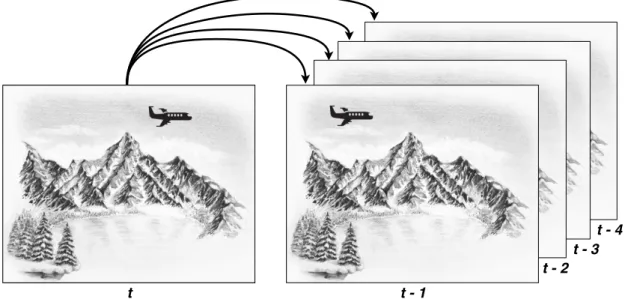
Motion prediction (inter-frame prediction) consists of motion estimation between consecutive frames. Once two consecutively frames are very likely to be similar, there is not a demand for encoding every pixel in the next frame again. This technique reduces memory occupation, being even more compression efficient than the spatial prediction [14]. As can be observed in Figure 2.4, the main goal of this technique is to decrease temporal redundancy.
t - 2 t - 3
t - 4
t t - 1
Figure 2.4: Example of Multi Reference Motion Estimation.
Then, for better motion prediction, each 16x16 MB can be split into 8x8, 8x4, 4x8 or 4x4 sub-macroblocks, also known as sub-mb-type [3]. The coding of such type of prediction is based on search areas, where the Block Motion Estimation (BME) is applied to predict movement in a rectangular block from the current frame. For this purpose, BME is used to compare neighboring MBs by applying a sum of the absolute difference in the compared areas [14].
2.1.3.3 MacroBlocks, Slices and Quantization Parameter (QP)
A division in MB and slices is a request by the H.264 standard to code the content. Typically, for video in 4:2:0 chroma sampling format, there is a demand for organizing the data in 16x16 matrices for luma (Y) and 8x8 for each chroma sample (U and V). It means that there is a request for unaligned memory accesses since a frame is usually saved in memory according to an interleaved or planar format, which can compromise the throughput of a system by making memory accesses less efficient.
Slices in H.264 serve the purpose of informing the encoder that the next MBs need to be spatially coded, not getting a reference of an earlier frame of the sequence. This type of slices is called I slices
[40]. In case of absence slice, the next MBs will be temporally coded.
The Quantization Parameter (QP) is applied to residual error data (the difference between prediction and the current MB), where an integer number is given to the encoder to define how much high frequencies data can be discarded. Since the human eye is less sensitive to higher frequency, we can increase the QP to reduce the information coded for high frequencies and thus reduce memory footprint [14].
2.1.3.4 Bitstream and NAL Unit
The bitstream is an important element of the encoder since it has all the relevant information to decode correctly the content. The H.264 standard was designed to support new possible features and higher video resolutions than those used by video systems at the releasing time of H.264. This problem led to the adoption of the Exponential Golomb universal code since it allows the header length to vary instead of being fixed to a given number of bits, difficulting a future upgrade of the encoder. In Table 2.2 is presented how a non-negative integer number can be coded in Exponential Golomb.
Table 2.2: Exponential-Golomb code words.
Integer Number
Binary Number
Exp-Golomb Number
0
0
1
1, 2
1, 10
010, 011
3, 4, 5, 6,
11, 100, 101, 110
00100, 00101, 00110, 00111
7, 8, 9, 10, ...
111, 1000, 1001, 1010
0001000, 0001001, 0001010, 0001011, ...
At the beginning of each frame file, there is always a predefined structure header, whose parameters are used by the decoder to correctly interpret and decode the video data. The SPS, PPS, and IDR are firstly identified by the header, enabling the later decoding of the payload. IDR stands for cleaning the picture references presented in the decoder buffer, consequently, the next frame needs to be spatially coded (intra-frame prediction) [3].
SPS PPS IDR
NAL NAL NAL
SLICE SLICE ...
DATA
HEADER
MB MB MB
Figure 2.5: H.264 Bitstream Structure.
Figure 2.5 presents the data structure of a bitstream resulting from H.264 encoding. SPS is coded along with the profile and level parameter, which allows the decoder to check if the profile and level are
supported, as they may contain some information about the application, maximum bit rate and maximum frame size [40]. If the profile or level is not supported the decoding may be rejected.
2.1.4
Peripheral Component Interconnect Express
PCIe is a high-performance bus interconnection for every platform these days. It allows high data rate communication for transfer applications between a host and a FPGA [41]. With the advancement of technology and the increasing amount of data speed buses, PCIe is becoming widely used and deployed in a large variety of Intel Architecture (IA) and non-IA platforms [11]. Estimations say that PCIe technology doubles data rate every three years [42]. Table 2.3 provides a bandwidth comparative analysis of each available PCIe generation.
Table 2.3: PCIe bandwidth for different generations and lane configurations, based on [11] and
[12].
Raw Bit Rate BW x1 BW x8 BW x16
PCIe 1.x 2.5 GT/s ∼250 MB/s ∼2 GB/s ∼4 GB/s
PCIe 2.0 5.0 GT/s ∼500 MB/s ∼4 GB/s ∼8 GB/s
PCIe 3.0 8.0 GT/s ∼1 GB/s ∼8 GB/s ∼16 GB/s
PCIe 4.0 16.0 GT/s ∼2 GB/s ∼16 GB/s ∼32GB/s
8k video at 60fps demands a data transfer rate equal to or higher than 15.9 GB/s by PCIe. Therefore, a PCIe technology below of Gen3.0 x16 or Gen4.0 x8 does not fulfill the requirements to equip video cards transmitting video with these characteristics in real-time.
2.2
Related Work
8k is still an emerging technology and, as a consequence, there are a few 8k-ready video cards available in the market. This section pretends to review some of these platforms, focusing on the ones similar to the video-card pretended to be developed during the MOG WALL SCREEN project, where this MSc thesis is inserted.
2.2.1
UHD Demosaicing on Low-Cost FPGA Pavel
The results exposed in [43], show that it is possible to process UHD video in a low-cost FPGA. Although this solution did not achieve a transfer of 8k in real-time, it is still an interesting solution since it was developed based on a low-cost FPGA and it is still able to treat 4k resolution video, contrasting the recommendation by Intel and Xilinx to choose high-cost FPGA like Arria, Stratix, Virtexand Kintex. According to the board specifications available in the market, it usually refers to higher operation frequency than it could achieve by testing in real conditions, which may be disappointed when passing the analysis to the design phase, as this paper describes. In addition, it can lead to money and time lost since sometimes it may be impossible to perform the needed System on-Chip (SoC) to accomplish the requested specifications. Despite this, the article describes this solution was deployed in the low-cost FPGA Intel Cyclone V. The broadcast interface is performed by a 12G-SDI video stream, whereas the color space used in the video transferring is RGB. The pixel clock is set at 596 MHz. Due to FPGA limitation cells that could not execute the tasks at an enough frequency to process the needed data, the solution taken ahead to accomplish the system has been by increasing parallelism. This technique may lead to a larger occupation of the board resources and consequently increased energy consumption. Therefore, the maximum frequency set for the FPGA programmable logic was 124.07 MHz.
2.2.2
AJA Kona IP
The AJA KONA IP supports only video resolutions up to 2k pixels. It can to communicate with a workstation by using the PCIe technology Gen2x8. The High Definition Multimedia Interface (HDMI) 1.4 is available for video connectivity. Moreover, it has two Small Form-factor Pluggable (SFP)+ connectors for input and output of video content. The broadcast interface is performed by a multi-link 3G SDI [4].
2.2.3
DELTA-3G-elp-tico-d 4C
The DELTA-3G-elp-tico-d 4Cis one of the two models available in the market provided byDeltaCast. It has four BNC connectors for the Quad-Link SDI interface. Additionally, it is possible to configure each BNC connector for supporting other video formats. The quad-link SDI interface enables the transmission of 4k video in YUV 4:2:2 with 10-bit color depth. The external communication is performed by a Gen2x8 PCIe data bus. [5].
Figure 2.7: Delta-3G-elp-tico-d 4C [5].
2.2.4
Magewell Pro Capture AIO 4K Plus
The Magewell Pro Capture AIO 4K Plus has one BNC connector for broadcast interface only with a Single-Link 6G SDI. It supports video transmission up to 4k at 60 fps by the HDMI 2.0 video interface. Additionally, this platform is equipped with PCIe Gen2 x4 technology, allowing data transfer rates up to 2 GB/s. [6].
Figure 2.8: Pro Capture AIO 4K Plus [6].
2.2.5
Bluefish444 Kronos Optikos
Even though theBluefish444has two video-Cards available in the market, theKronos Optikosseems to be the most complete solution, when compared with the Kronos Electronversion. This platform has an octa-link 3G SDI interface available for video transmission, supporting up to 4k video resolutions.
Some 8k video formats may also be supported by this board, in spite of being a little restricted in this aspect. This board is equipped with an HDMI 2.0 interface, already supports the transmission of 4k video. Additionally, it has three broadcast interfaces available, two for SFP+ and one Dual-Link 3G SDI along with BNC connectors [7]. The PCIe technology available on this board is the
Figure 2.9: Bluefish444 Kronos Optikos [7].
2.2.6
Dektec DTA-2179
TheDektec DTA-2179presents a higher number of BNC connectors (twelve), where each one can be configured individually for input or output by software. From this set of BNC connectors, only eight support 3G-SDI, which limits the number of 3G-SDI connections following a quad-link topology to two. This board is available with PCIe Gen3x16 technology, allowing data transfer rates capable of handling 8k video in real-time. However, unlike the SDI technology provided, the remaining components that are part of this video-card seem to be short to accomplish 8k video. Nevertheless, it is able for transmitting up to 4k video [8].
2.2.7
Discussion
Table 2.4 summarizes the most relevant specifications of the video boards reviewed during this section. Table 2.4: Characteristics summary of the analyzed Video-Cards.
Name
Video
Interfaces
Broadcast
Interfaces
Data
Bus
4k/
8k?
UHD Demosaicing on Low-Cost
FPGA Pavel
BMC
Single-Link 12G SDI
–
4k
AJA Kona IP
HDMI 1.4
Multi-link 3G SDI
Gen2x8
–
DELTA-3G-elp-tico-d 4C
BMC
Quad-link 3G SDI
Gen2x8
4k
Pro Capture HMDI 4K Plus
HDMI 2.0
Single-link 6G SDI
Gen2x4
4k
Bluefish444
Kronos Optikos
HDMI 2.0
2 SFP+ &
Dual-link 3G SDI
Gen3x8
8k/
4k
DTA-2179
BMC
Octa-link 3G SDI
Gen3x16
4k
From the set of boards reviewed, Dektec DTA-2179 presents the most powerful PCIe technology. Its PCIe Gen3x8 and x16 are solutions already able to handle the data rate demanded by 8k video transmission. On the other hand, the remaining technologies presented seem to be a little short. The presence of HDMI 2.0 is also a valuable resource since this HDMI version is already able for transmitting up to 4k video in raw format and even 8k in some compressed video formats.
Bluefish444 Optikosseems to be the only option able for treating 8k video in raw format due to the two SFP+ and the Octa-Link 3G SDI available. The bottleneck of this video card resides in the PCIe technology adopted, as PCIe Gen3x8 does not have sufficient throughput to handle 8k video in raw format. From this review, it can be easily spotted the gap in the industry that this MSc thesis pretends to tackle.
In this chapter is presented the design phase behind the reconfigurable hardware for a new generation IoT video-card. It will be presented and discussed the design of some critical points to achieve as much as possible throughput to guarantee the proposed goal of 8k at 60fps. The design phase will focus only on the modules aimed to this MSc thesis, namely on Memory Manager and H.264 Encoder.
3.1
Development Environment
This chapter presents the tools and platforms used in the development of the work inherent to this MSc thesis. Some tools are requirements of the project, whereas others are used just for convenience. Both tools are summarized in this chapter, being highlighted its main features.
3.1.1
Zynq UltraScale+ MPSoC ZCU102
The Xilinx UltraScale+ architecture allows multi-hundred gigabit-per-second levels of performance for efficient routing design and data processing in an SoC. The ZCU102 board is based on the Zynq UltraScale+ XCZU9EG-2FFVB1156E Multi Processor System on Chip (MPSoC), which combines PL with a powerful PS, as depicted in Figure 3.1.
Figure 3.1: Zynq UltraScale+ MPSoC Overview Block Diagram [9].
The Processing System features the Arm flagship Cortex-A53 64-bit quad-core processor and Cortex-R5 dual-core real-time processor, with 256 KB of on-chip memory and 4 GB of Random-Access Memory (RAM) (DDR4). This PS is also equipped with general-purpose I/O and interfaces that establish a connection with the PL part of the board. The connection interfaces provided along with this PS are detailed in Figure 3.2. The resources available on the PL side are summarized in Table 3.1.
Chapter 3. System Specification 23
Zynq UltraScale+ MPSoC Base TRD 7
UG1221 (v2019.1) May 31, 2019 www.xilinx.com
Zynq UltraScale+ MPSOC Overview
The Zynq device is a heterogeneous, multi-processing SoC built upon the 16 nm FinFET process node from TSMC. Figure 1-1 shows a high-level block diagram of the device architecture and key building blocks inside the processing system (PS) and the programmable logic (PL).
The following summarizes the MPSoC’s key features:
• Application processing unit (APU) with 64-bit quad-core ARM Cortex-A53 processor • Real-time processing unit (RPU) with 32-bit dual-core ARM Cortex-R5 processor • Multimedia blocks
° Graphics processing unit (GPU), ARM Mali-400MP2 ° Video encoder/decoder unit (VCU) up to 4K 60 fps ° DisplayPort interface up to 4K 30 fps
X-Ref Target - Figure 1-1
Figure 1-1: Zynq UltraScale+ MPSoC Block Diagram
UG1221_062316
Zynq UltraScale+ MPSoC Processing System
Application Processing Unit Memory High-Speed
Connectivity
GIC-400 SCU CCI/SMMU 1MB L2 w/ECC ARM® Cortex™-A53 NEON™ Floating PointUnit 32KB I-Cache w/Parity 32KB D-Cache w/ECC Memory Mgmt Unit Trace Macro Cell
Real-Time Processing Unit
2 1
34
Graphics Processing Unit ARM Mali™-400 MP2 Geometry
Processor
Two Pixel Processors
Memory Management Unit 64KB L2 Cache DDR4/3/3L, LPDDR4/3 ECC Support 256KB OCM with ECC DisplayPort USB 3.0 SATA 3.1 PCIe Gen2 PS-GTR 2 GIC ARM
Cortex-R5 Memory Protection Unit Vector Floating Point Unit
128KB TCM w/ECC 32KB D-Cache w/ECC 32KB I-Cache w/ECC Trace Macro Cell 1 Configuration & Security Unit Config AES Decryption, Authentication, Secure Boot DMA, Timers, WDT, Resets,
Clocking, and Debug TrustZone
Voltage/Temp Monitor Platform Management Unit System Control System Management Power SD/eMMC NAND Quad SPI NOR
SPI UART
CAN GigE
Zynq UltraScale+ MPSoC Programmable Logic
Storage & Signal Processing Block RAM UltraRAM DSP General-Purpose I/O High-Performance HP I/O High-Density HD I/O High-Speed Connectivity GTH GTY Interlaken 100G EMAC PCIe Gen4 Video Codec H.265/H.264 System Monitor General Connectivity Send Feedback
Figure 3.2: Zynq UltraScale+ MPSoC PS and PL Block Diagram [9].
Table 3.1: Zynq UltraScale+ MPSoC ZCU102 Features and Resources [9].
Feature Resource Count
System Logic Cells 599 550
CLB Flip-Flops 548 160
CLB LUTs 274 080
HD banks 5 banks, total of 120 pins
HP banks 4 banks, total of 208 pins
MIO banks 3 banks, total of 78 pins
PS-side GTR 6 Gb/s transceivers 4 PS-GTRs PL-side GTH 16.3 Gb/s transceivers 24 GTHs
Max. distributed RAM 8.8 Mb
Block RAM Blocks 912
Total block RAM 32.1 Mb
DSP slices 2 520
Additionally, there are a set of tools for deployment assistance. Xilinx Vivado Design Suite and Xilinx Software Development Kit (SDK) are Integrated Development Environments (IDEs) of Xilinx for hardware
and software development, respectively. The Xilinx Vivado Design Suite is a software suite for the analysis and synthesis of HDL designs. This IDE even provides an IP library, with a bunch of soft cores which can be mixed with or be part of user-made IP cores. The Xilinx SDK enables the development of embedded applications for the PS part of the board.
Besides the substantial set of resources available shown in the MPSoC diagram, there are a few crucial interfaces for the PS-PL communication, which allows not only data interchanging with memory but also eventual reconfiguration for IP cores.
3.1.1.1 Master Interfaces PS-PL
There are three AXI High Performance Master PS-PL interfaces allowed in the SoC. Each interface can be configured to operate in 32-bit, 64-bit, and 128-bit data widths [44].
• AXI HPM0 FPD and AXI HPM1 FPD - Two high performance master interfaces for full-power domain. • AXI HPM0 LPD - High performance master for low-power domain.
Each slave interface supports 32-bit, 64-bit, and 128-bit data widths [44].
3.1.1.2 Slave Interfaces PS-PL
• AXI HPC0 FPD, AXI HPC1 FPD - Two high performance coherent slave interfaces for full-power domain.
• AXI HP0 FPD, AXI HP1 FPD, AXI HP2 FPD, AXI HP3 FPD - Four high performance slave interfaces for full-power domain.
• AXI LPD - One slave interface for low-power domain.
• AXI ACP - One Accelerator Coherency Port slave interface that can be connected to a DMA engine or a non-cached coherent master.
3.1.2
AMBA Advanced eXtensible Interface
Advanced Microcontroller Bus Architecture (AMBA) AXI protocol is an open-standard introduced by ARM and its scope aims the design of high-performance and high-frequency systems for data interchanging [13]. Some key features that makes of AXI a reliable protocol are:
• Support for unaligned data transfers by using byte strobes signal; • Write and read address validation before the data transaction;
• Allows transmission of data in burst mode, in which only the start address is needed for up to 256 or other power of two (2n) number of words being transferred in a row;
• Read and write channels are independent [13].
Figure 3.3 represents the data interchanging timing order inherent to AXI4-Memory Mapped read and write operations. As can be observed, both operations occur in independent buses. Both Read and Write channels are independent of each other, they have not only different channels but also independency in the protocol level. Moreover, the Figure 3.3 pretends to represent the data interchanging timing order of each sub-channels of Read and Write channels.
Master Interface Address and Control Read Data Read Data Read Data Read Data Read Channel Read Address Channel
Read Data Channel
Address and Control Write Data Channel
Write Data Write Data Write Data Write Data
Write Response Channel Write Response
Write Address ChannelWrite Channel Slave
Interface
Figure 3.3: Timing diagram for AXI4-Memory Mapped read and write operations.
3.1.2.1 AXI4-Memory Mapped
AXI4 is a data transaction protocol designed for memory mapped interfaces. It allows to burst up to 256 data transfer cycles with a single address phase, both for read and write operations. Each AXI
interface uses a single clock signal (ACLK). The data is accepted or transferred on the rising edge. The reset signal in the AXI (ARESETn) takes effect driven in low. Whereas the reset assertion may happen asynchronously, deassertion must occur synchronously with the rising edge ofACLK[13].
3.1.2.1.1 Read Channel
Figure 3.4: AXI4 Read channel timing diagram [10].
According to Figure 3.4, the reading address is accepted by the slave only whenARVALIDandARREADY
are set high. The former signal indicates whether the address issued by the master is valid, while the latter indicates whether the slave is ready to accept a read address. As expected, a read address is only accepted when the slave is ready to accept it and the master issues a valid one. In Table 3.2 are listed all the signals required for address acceptance.
Table 3.2: AXI4 Read address channel signals [13].
Signal Description Source Required?
AXI4-Lite?
ARID[3:0] Read address ID Master Optional No
ARADDR[a− 1:0] Read address Master Required Yes
ARLEN[3:0] Burst length Master Optional No
ARSIZE[2:0] Burst size Master Optional No
ARLOCK[1:0] Lock type Master Optional No
ARCACHE[3:0] Cache type Master Optional Yes
ARVALID Read address valid Master Required Yes
After the address being accepted by the slave, the master starts reading the data issued by the slave. The process moves forward only whenRREADYandRVALIDare set high. WhileRVALIDis set by the master to inform the slave of the existence of valid data in the channel,RREADYis driven by the salve to inform the master it is ready to receive new data. AlthoughRLASTis optional, its use is highly recommended for detecting whenever misalignment between master and slave occurs. Table 3.3 shows the signals needed for the read data stage [45].
Table 3.3: AXI4 Read data channel signals [13].
Signal Description Source Required?
AXI4-Lite?
RID[3:0] Read data ID Slave Optional No
RDATA[n− 1:0] Read address Slave Required Yes
RRESP[1:0] Burst length Slave Optional No
RLAST Read last Slave Optional No
RUSER Read User Slave Optional No
RVALID Read valid Slave Required Yes
RREADY Read ready Master Required Yes
3.1.2.1.2 Write Channel
The write channel (Figure 3.5) acts similarly to the read channel. The difference resides in the feedback required in the write channel through the write response channel. In this particular stage of the communication, the slave signals the master the success or not of the operation byBRESP. The write response is only accepted when both BVALIDand BREADYare set high. The Write Channel is divided in three different sub-channels that communicate in different stages. Similarly to the read address channel, a write address is only accepted by the slave when theAWVALID andAWREADYsignals are driven high. The remaining signals used to validate an address are detailed in Table 3.4.
Table 3.4: AXI4 Write address channel signals [13].
Signal Description Source Required? AXI4-Lite
AWID[3:0] Write address ID Master Optional No
AWADDR[a− 1:0] Write address Master Required Yes
AWLEN[3:0] Burst length Master Optional Yes
AWSIZE[2:0] Burst size Master Optional No
AWLOCK[1:0] Lock type Master Optional No
AWCACHE[3:0] Cache type Master Optional Yes
AWVALID Write address valid Master Required Yes
AWREADY Write address ready Slave Required Yes
In the write data stage, is where the data is transferred from the master to the slave upon theAWLEN. In the last data transaction, analogously to the read data channel, the WTLASTis asserted high. In case thatWSTRBis not set all bits high, only the N least significant bytes shall be passed to the memory in each instant [13]. The signals inherent to the data transaction stage are detailed in Table 3.5.
Table 3.5: AXI4 Write data channel signals [13].
Signal Description Source Required? AXI4
Lite?
WDATA[n− 1:0] Write data Master Optional Yes
WSTRB[3:0] Write strobes Master Required Yes
WLAST Write last Master Optional No
WVALID Write valid Master Required Yes
Finally, the write response provides the master a feedback from the slave of the transaction state. Only theBRESPis optional in the protocol. Table 3.6 details the signals present in the write response channel.
Table 3.6: AXI4 Write response channel signals [13].
Signal Description Source Required?
AXI4-Lite?
BID[3:0] Response ID Slave Required No
BRESP[1:0] Write response Slave Optional Yes
BVALID Write response valid Slave Required Yes
BREADY Response ready Master Required Yes
3.1.2.2 AXI4-Stream
Stream does not require an address phase and it also allows unlimited data burst size. AXI4-Stream does not have an address since it is not intended for memory-mapped purposes [45]. Even though
TREADYis optional, it is highly recommended for ensure that the slave is ready for receive data and that it was also accepted [45]. BothTLASTandTUSERsignals, detailed in Table 3.7, are optional but sometimes it may be a useful, depending on the system, to inform the slave the occurrence of an event.
Table 3.7: AXI4-Stream channel signals [13].
Signal Description Source Required?
TVALID Transfer valid Master Required
TREADY Transfer ready Slave Optional
TDATA[v− 1:0] Transfer data Master Required TSTRB[3:0] Transfer strobes Master Optional
TKEEP[3:0] Valid bytes Master Optional
TLAST Response ready Master Optional
TID[i− 1:0] Response ready Master Optional TDEST[d− 1:0] Response ready Master Optional TUSER[u− 1:0] Response ready Master Optional
3.1.2.3 AXI4-Stream Video
AXI4-Stream Video is a variant of the AXI4-Stream protocol designed for video transmission purposes. When compared to the basic protocol, AXI4-Stream Video uses two additional signals. Whereas theTLAST
signal notifies the slave that the current data being transmitted is the end of a line, theTUSERserves to inform the slave about the start of a new frame. Both signals give some information that may be important to detect when errors may occur, for instance, when the slave is tracking the number of pixels received from master and it does not match with the pre-configured data.
3.1.2.4 AXI4-Lite
AXI4-Lite is a light-weight, single transaction for memory-mapped purpose. It has a simple interface and a small logic footprint. [45]. In Tables 3.2, 3.3, 3.4, and 3.5 are shown the signals used by AXI4-Lite. The protocol acts the same way as described for the write and read channels of AXI4-Memory Mapped, however, with a limit of one transaction per address phase.
3.2
IoT Video-Card Architecture
The MOG WALL SCREEN project, in which this MSc thesis is inserted, has already a predefined general architecture defined in Figure 3.6. This figure already contemplates some residual changes that were added during the deployment of this work. This IoT Video-Card has been designed to accomplish 8k video acquisition and reproduction in real-time. Besides the demand for a video-card ready for reconfigurable video characteristics (resolution, fps) on-the-fly, there is also a requirement for deployment of reconfigurable hardware to enable and ease the process of future system updates. Next it will be given an overview of the general architecture of the video-card, in which it will be explained the aim for each core. Then, this thesis will be focusing on the aim for this thesis, the Memory Manager and H.264 Encoder.
Figure 3.6: HDL General Architecture of the Reconfigurable Video-Card.
SMPTE UHD-SDI Subsystem
This IP core is available fromXilinxand is responsible for the interaction between the remaining video-card IP cores and the hardware transceivers, which support the transfer rates required to carry video up to 8K resolution at 30 fps.
SDI SerDes
The SDI Serializer Deserializer is responsible for synchronizing the streams coming from the four IP core SMPTE UHD-SDI instances. The total sum of video streams is 64, 16 per channel. The product of this module is a stream containing the video content from each one of the 16 channels. This stream will be redirected to Memory Manager, which is in charge of performing memory accesses.
![Figure 2.1: Required bit rate to transmit various video formats [1].](https://thumb-eu.123doks.com/thumbv2/123dok_br/17231980.787046/24.892.111.784.195.388/figure-required-bit-rate-transmit-various-video-formats.webp)
![Figure 2.2: AXI VDMA Block Diagram (Adapted from [2]).](https://thumb-eu.123doks.com/thumbv2/123dok_br/17231980.787046/27.892.177.718.122.329/figure-axi-vdma-block-diagram-adapted-from.webp)
![Figure 2.3: Intra-prediction modes for 4x4 MB[3].](https://thumb-eu.123doks.com/thumbv2/123dok_br/17231980.787046/31.892.205.694.121.502/figure-intra-prediction-modes-for-x-mb.webp)
![Table 2.3: PCIe bandwidth for different generations and lane configurations, based on [11] and [12].](https://thumb-eu.123doks.com/thumbv2/123dok_br/17231980.787046/34.892.203.685.522.695/table-pcie-bandwidth-different-generations-lane-configurations-based.webp)
![Figure 3.1: Zynq UltraScale+ MPSoC Overview Block Diagram [9].](https://thumb-eu.123doks.com/thumbv2/123dok_br/17231980.787046/40.892.184.713.118.776/figure-zynq-ultrascale-mpsoc-overview-block-diagram.webp)


![Table 3.2: AXI4 Read address channel signals [13].](https://thumb-eu.123doks.com/thumbv2/123dok_br/17231980.787046/44.892.190.700.791.1132/table-axi-read-address-channel-signals.webp)
![Figure 3.5: AXI4 Write channel timing diagram [10].](https://thumb-eu.123doks.com/thumbv2/123dok_br/17231980.787046/45.892.170.724.765.1049/figure-axi-write-channel-timing-diagram.webp)