94 Brazilian Journal of Physics, vol. 33, no. 1, March, 2003
Electron Field Emission Measurements
from Boron-Doped CVD Diamond on Tantalum
J. A. N. Gonc¸alves, G. M. Sandonato,
Laborat´orio Associado de Plasma, Instituto Nacional de Pesquisas Espaciais
Caixa Postal 515, CEP 12201-970, S˜ao Jos´e dos Campos, SP, Brazil
and K. Iha
Instituto Tecnol´ogico de Aeron´autica, Departamento de Qu´ımica
12228-900, S˜ao Jos´e dos Campos, SP, Brazil
Received on 12 March, 2002. Revised version received on 2 August, 2002
Boron-doped polycrystaline diamond films grown by hot-filament-assisted chemical vapor deposition were studied with ultraviolet photoemission spectroscopy (UPS), Raman spectroscopy, X-ray diffractometry and current voltage measurements. The UPS measurement shows that the work function () without electric field
is about 3.9eV. The field-emission current-voltage measurements indicate a threshold voltage ranging from
8.97x10⁶
to 9.64x10⁶
V=m and a work function () about 0.3eV. These results show that boron doped
diamond films exhibit a negative electron affinity in high electric field.
I
Introduction
Diamond possesses unique semiconductor properties, such as wide bandgap, high breakdown voltage, and both high electron and hole mobilities [1]. These properties make dia-mond attractive for application in frequency and high-power electronics. Boron doped diamond films have been prepared by various chemical vapor deposition (CVD) meth-ods and some works have provided information on the struc-tural, optical an electrical properties of the films [2-8].
Boron doped diamond is a p-type semiconductor, and it is the only dopant which has been successfully and repro-ducible used to prepare semiconductor diamond. Because of its small size, the boron atom is easily incorporated in the diamond lattice. The introduction of boron atoms would af-fect the structure and properties of the diamond films, so it is important to understand the nature of boron atoms in the diamond films for preparing semiconductor diamond.
In the present work, polycrystalline diamond films with high boron concentration were prepared on tantalum sub-strate by hot filament CVD method. The boron was intro-duced by B2O3in methanol solution.
Scanning electron microscopy (SEM) and x-rays diffrac-tometry (XDR) were employed to study the morphology and structure of these films. Raman spectroscopy, current-voltage characteristics (IvsV) and ultraviolet
photoemis-sion spectroscopy (UPS) were used to investigate their opti-cal and electriopti-cal properties.
II
Experimental details
The diamond films were grown on monocrystalline tanta-lum (111) by hot filament CVD in a 10mdiameter and 30
mhigh cylindrical quartz reactor. Boron was introduced in
the reactor by flowing hydrogen through the B2O3methanol
solution.
The substrates were previously cleaned with acetone and scratched by a diamond paste (grain size of 1m) in order
to promote a better nucleation of the diamond films. The di-amond films were grown at 800o
Cfrom 0.5%H
2/CH4
mix-ture at a total pressure of 50Torr. Boron oxide in methanol
solution was used with 20000ppmB/C ratio.
A spectroscope Renishaw model RM 3000 was used for Raman spectroscopic investigations with an air cooled 785
nm laser diode (with an output power of 17Mw) for
ex-citation of the samples. The diffractograms were obtained using a spectrometer Phillips PW 1840 X-ray with a solid state goniometer, and equipped with CuKa (1.5406) cath-ode and nickel filter. The control parameters for the samples investigated are shown in Table 1.
Table 1. X-ray parameters for the sample investigated.
Power 40 KV e 250 mA
Step size(2) 0.020
Number of steps 5500 Time per steps( s) 1.00
Scan speed(2=s) 0.02
J.A.N. Gonc¸alves, G.M. Sandonato, and K. Iha 95
The first type of electron emission measurement em-ployed was UPS wherein the ultraviolet light is incident on the conduction band [9]. Electrons with sufficient energy to overcome the electron affinity of the material are emitted into the vacuum. The second type of electron emission mea-surement was current-voltage characteristics(IV). The
I V measurements were taken at two distances using an
experimental setup specially developed to this purpose.
III
Results
The surface of the diamond film was observed by scanning electron microscopy (SEM). Figure 1 shows SEM micro-graph of surface morphologies for boron doped diamond deposited on tantalum. Crystal facets are observed with a thickness of 15mand grain sizes are 2m. Both thickness
and grain sizes were obtained by SEM microscopy.
Figure 1. Scanning Electron Microscopy (SEM) of diamond film
grown with B/C of 20000ppm.
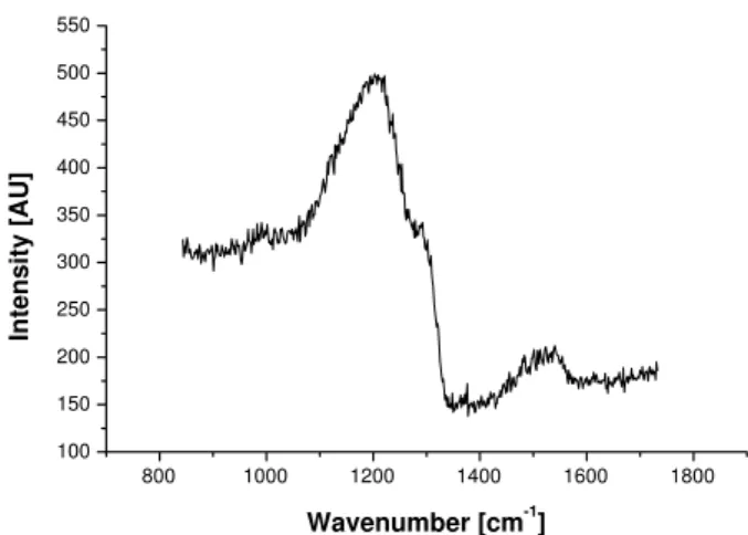
Since Raman spectroscopy is a nondestructive method, it is commonly used in characterization of the structure and quality of synthesized diamond films [10]. A drastic change of Raman spectra of diamond film with high level of boron was observed. The results reveal that the peak intensity at 1332m
1
, corresponding to the transversal mode (related to the sp
3
bound) of the diamond, decreases as the boron concentration increases [11]. Nevertheless, a wide band arises around 1220 m
1
and increases as the boron con-centration is increased, as shown in Fig. 2.
The same sample was investigated by x-ray diffractom-etry and the peaks related to the tantalum, tantalum carbide and diamond are shown in Figure 3. Although the tantalum substrate has no any preferential growing direction, it can be noted that the diamond peak of the plane (111) is more intense than the peak of the plane (220). This indicates that the growing process occurs preferentially at the plane (111), otherwise the orientation of the diamond films should be in the plane (110), i.e., in the transversal plane to the plane (111).
800 1000 1200 1400 1600 1800
100 150 200 250 300 350 400 450 500 550
Intensity [AU]
Wavenumber [cm-1]
Figure 2. Raman spectroscopy of diamond films grown with B/C of 20000ppm.
0 20 40 60 80 100 120
0 2000 4000 6000 8000 10000 12000
Diam
(311) Ta (422)
TaC (420) TaC (331) Ta (310) Ta (220)
Diam (220) Ta (211)
TaC (220) Ta (200)
Diam (111) TaC (200) Ta (110)
TaC (111)
Intesity, UA
2q (degree)
Figure 3. Typical XDR diffractogram of diamond film on tanta-lum.
UPS measurements were performed in the Link¨oping University, in an ultra high vacuum chamber (base pressure below 2x10 10
Torr). The sample excitation in this system
was provided by 21.5eV light a helium resonance discharge
lamp, and a hemispherical analyzer was used to measure the energy spectrum of the photoemitted electrons.
The UPS system is described in more details elsewhere [12]. The work function measured was 3.9eV for the boron
doped diamond film.
Field emission measurements were obtained within high vacuum chamber (background pressure bellow 10 5
Torr)
and the measurements were performed in the characteriza-tion system. The sample was placed and held in the proper compartment, and the movable anode was used for distance adjustment. The current-voltage measurements, taken at 50
m and at 100m apart from the cathode are shown in
Figure 4. The sample area probed was the 10mm in
di-ameter. Field emission current-voltage measurement indi-cates threshold voltages of 8.97x10⁶
V=mfor 50m and
9.64x10⁶
96 Brazilian Journal of Physics, vol. 33, no. 1, March, 2003
200 250 300 350 400 450 500 550 600 650 700 750 800 850 900 950 0,0 0,2 0,4 0,6 0,8 1,0 CURRENT ( m A) VOLTAGE (V) 50mm 100mm
Figure 4. Current-voltage characteristics ploted as linearIvsV at
room temperature.
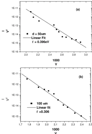
These field emission results can be analyzed in terms of Fowler-Nordheim theory which describes the electron emission current via barrier tunneling [13]. The Fowler-Nordheim equation has the form:
I =k V d 2 exp 6530d 3 2 V !
wherekis a constant related to the emission area,V is the
voltage applied,is the work function,is the geometric
field enhancement factor anddis the distance from anode
to the cathode. The experimental values ofln(IV 2
) were plotted againstV
1
, and the slope of the straight line gives the work function () values of 0.396 and 0.306eV for the
distances of 50mand 100m, respectively, as shown in
Fig. 5. The work function values obtained are in agreement with the emission characteristics of boron doped diamond cathodes [13].
IV
Conclusion
The downshifts of both Raman peaks at 1332m 1
and at 1220m
1
were attributed to the boron incorporation in the diamond film. The investigations by X-ray diffractometry have revealed the occurrence ofTaC in the diamond film
and the growing process occurs preferentially at the plane (111), as shown in Fig. 3.
Ultraviolet photoemission spectroscopy (UPS) indicates the sample posses work function of the 3.9eV with no
elec-tric field applied. When an intense elecelec-tric field is applied, the work function downshifts to 0.3eV. This fact shows that
the boron doped diamond film exhibits field emission com-portment with threshold voltages ranging from 8.97x10⁶
to 9.64x10⁶
V=m, for the cathode/anode distances of 50 m
and 100mrespectively.
2,0 2,2 2,4 2,6 2,8 3,0
1E-16 1E-15 1E-14 1E-13 1E-12 1E-11 (a)
d = 50mm
Linear Fit f = 0.396eV I 2V
1000 V
1,7 1,8 1,9 2,0 2,1 2,2 2,3 2,4 2,5
1E-15 1E-14 1E-13 1E-12 1E-11 (b)
100 mm
Linear fit
f =0.306
I 2V
1000 V
Figure 5. Fowler-Nordheim plot of the field emission (a) for 50
m distance cathode-anode and (b) for 100m distance
cathode-anode.
Acknowledgement
We would like to express our thanks to Dr E. J. Corat and V. T. Airoldi for their help in the synthesis of diamond films.
This work has been supported by the Fundac¸˜ao de Am-paro a Pesquisa do Estado de S˜ao Paulo (FAPESP)
References
[1] J. Wilks and E. Wilks,Properties an Application of Diamond, Butterworth-Heinemann, Oxford, 1991.
[2] J. Mort, M. A. Machonkin, and K. Okumura, Appl. Phys. Lett.58, 1908 (1991).
[3] K. Nishimura, K. Das, and J. T. Glass, J. Appl. Phys.69, 3142 (1991).
[4] X. H. Wang, G. H. M. Ma, W. Zhu, J. T. Glass, L. Bergman, K. F. Turner, and R. J. Nemanich, Diamond Related Mater.1, 828 (1992).
[5] Y. San, Z. Guangtian, and J. Zengsun, Chin. J. Semicond.14, 580 (1993).
[6] M. Werner, O. Dorsch, H. U. Baerwind, E. Obermeier, L. Haase, W. Seifert, A. Ringhandt, C. Johnston, S. Romani, H. Bishop, and P. R. Chalker, Appl. Phys Lett.64, 595 (1994).
[7] R. Locher, J. Wagner, F. Fuchs, M. Maier, P. Gonon, and P. Koidl, Diamond Rel. Mater.4, 678 (1995).
J.A.N. Gonc¸alves, G.M. Sandonato, and K. Iha 97
[9] A. Zangwill, Physics at Surfaces, Cambridge University
Press, Cambridge, 1998.
[10] K. Miyata, K. Kumagai, K. Nishimura, and K. Kobashi, J. Mater. Res.8, 35 (1993).
[11] L. H. Robins, E. N. Farabaugh, and A. Feldiman, In Dia-mond Optics IV, 22-23 July 1991, San Diego, CA.
Belling-ham, Wash. SPIE, 105.
[12] J. van der Weide, Z. Zhang, P. K. Baumann, M. G. Wensell, J. Bernholc, and R. J. Nemanich, Phys. Rev. B50, 5803 (1994).