Universidade de Aveiro 2011
Departamento de Física
Pedro Manuel
Parracho Salomé
Filmes Calcogenetos para células solares:
Crescimento e Propriedades
Chalcogenide Thin Films for Solar Cells: Growth
and Properties
Universidade de Aveiro 2011
Departamento de Física
Pedro Manuel
Parracho Salomé
Filmes Calcogenetos para células solares:
Crescimento e Propriedades
Chalcogenide Thin Films for Solar Cells: Growth and
Properties
Dissertação apresentada à Universidade de Aveiro para cumprimento dos requisitos necessários à obtenção do grau de Doutor em Física, realizada sob a orientação científica do Doutor António F. da Cunha, Professor Auxiliar do Departamento de Física da Universidade de Aveiro.
There's no certainty - only opportunity. V, 2006
o júri
presidente Prof. Doutor José Joaquim de Almeida Grácio
professor catedrático da Universidade de Aveiro
Prof. Doutor António Manuel Barros Gomes de Vallêra
professor catedrádico aposentado da Faculdade de Ciências da Universidade de Lisboa
Prof. Doutor Alessandro Romeo
assistant professor, Faculty of Science, University of Verona
Prof. Doutor Hugo Manuel Brito Águas
professor auxiliar da Faculdade de Ciências da Universidade Nova de Lisboa
Prof. Doutor Antonio Ferreira da Cunha professor auxiliar da Universidade de Aveiro
acknowledgements
I would like to thank Professor António F. da Cunha for accepting me to be his student and for his teachings. I also would like to thank Professor Celeste do Carmo for encouraging me to continue my studies and for accepting me in the I3N as a Ph.D. student.
I acknowledge and appreciate the acceptance of Professor António Vallêra, Professor Hugo Águas and Professor Alessandro Romeo for being part of the jury of this thesis.
I have to thank several people for their technical and social support: Eng.ª Marta Ferro for the help with SEM; Doctor Rosário Soares for the help with the XRD measurements; Professor Rosário Correia for being always available to help dealing with the Raman system and the talks about the institution and life in general; António Fernandes for the help with the Raman system; Miguel Rocha and Ivo Mateus for the technical help in the workshop; Professor Juan Gonzales for the talks, the support and the measurements done in Minas Gerais; Professor Joaquim Leitão for the PL measurements and for listening to my usual disagreements regarding the decay of the institution as a team; Doctor Alfons Weber, Ing. Björn Schubert and Christiane Stephan for receiving me in Berlin and for the comradeship; Professor Armando Lourenço for the good company in the laboratory; Emanuel Santos for the help with some images and the good coffee at FISUA; Francisco Reis for the help with IT; last but not the least, all my laboratory colleagues during the time of work that lead to this thesis: Fábio Vinagre, Catarina Cardoso, Gabriela Cardoso, Isabel Fernandes, Paulo Fernandes, André Sartori, João Malaquias, Mário Lima and Marta Ferreira.
My mother, my father and my São-Marcos family including my sister for supporting me in the good and in the bad days.
FCT and Fundação Gulbenkian for the financial support. Many others could be mentioned, for those a sincere thank you.
Above all, thank you Ana for your warmth and love. Without you, I would have struggled much more to keep going. You listened patiently when was needed, talked harsh when was needed, proofread part of this thesis but most
importantly always stayed on my side. Having you makes it all worthwhile.
Finally, a special thank you for the I3N, the University and the Physics
department secretariat for not letting this adventure going without the joy of all the administrative stuff.
keywords Solar cells, thin films, chalcogenides, Cu(In,Ga)Se2, CIGS, Cu2ZnSnSe4, CZTSe, Cu2ZnSn(S,Se)4, CZT(S,Se), hybrid system, growth and characterization of semiconductors.
abstract Thin film solar cells have in recent years gained market quota against traditional silicon photovoltaic panels. These developments were in a large part due to CdTe solar panels on whose development started earlier than their competitors. Panels based on Cu(In,Ga)Se2 (CIGS), despite being more efficient in a laboratory and industrial scale than the CdTe ones, still need a growth technology cheaper and easier to apply in industry. Although usually presented as a good candidate to make cheap panels, CIGS uses rare and expensive materials as In and Ga. The price evolution of these materials might jeopardize CIGS future.
This thesis presents three different studies. The first is the study of different processes for the incorporation of Ga in a hybrid CIGS growth system. This system is based on sputtering and thermal evaporation. This technology is, in principle, easier to be applied in the industry and solar cells with efficiencies around to 7% were fully made in Aveiro.
In the second part of this thesis, a new material to replace CIGS in thin film solar cells is studied. The growth conditions and fundamental properties of Cu2ZnSnSe4 (CZTSe) were studied in depth. Suitable conditions of temperature and pressure for the growth of this material are reported. Its band gap energy was estimated at 1.05 eV and the Raman scattering peaks were identified. Solar cells made with this material showed efficiencies lower than 0.1%.
Finally, preliminary work regarding the incorporation of selenium in Cu2ZnSnS4 (CZTS) thin films was carried out. The structural and morphological properties of thin films of Cu2ZnSn(S,Se)4 have been studied and the results show that the incorporation of selenium is higher in films with precursors rather with already formed Cu2SnS3 or Cu2ZnSnS4 thin films. A solar cell with 0.9 % of efficiency was prepared.
palavras-chave Células solares, filmes finos, calcogenetos Cu(In,Ga)Se2, CIGS, Cu2ZnSnSe4, CZTSe, Cu2ZnSn(S,Se)4, CZTSSe, crescimento e caracterização de filmes finos.
resumo As células solares de filmes finos têm nos últimos anos ganho cota de mercado aos tradicionais painéis fotovoltaicos de Silício. Estes desenvolvimentos devem-se em grande parte ao painéis baseados em CdTe cujo desenvolvimento começou mais cedo que os seus competidores. Os painéis baseados em Cu(In,Ga)Se2 (CIGS), apesar de serem mais eficientes tanto numa escala industrial como em laboratório, necessitam de uma tecnologia de crescimento que seja barata e de fácil aplicação na indústria. Apesar de se apresentarem como um bom candidato para painéis baratos o CIGS usa materiais caros e raros na crosta terrestre como o In e o Ga. A evolução do preço destes materiais podem comprometer o seu futuro.
Nesta tese são apresentados três estudos diferentes. O primeiro é o estudo de diferentes processos de incorporação de Ga em CIGS crescido por um sistema híbrido de pulverização catódica e evaporação térmica. Esta tecnologia é, em princípio, mais fácil de ser aplicada a nível industrial e células solares feitas em Aveiro com eficiências próximas dos 7% foram produzidas.
Numa segunda parte, outro material cujas propriedades o aponta como possível substituto ao CIGS é estudado. As condições de crescimento e propriedades fundamentais do Cu2ZnSnSe4 (CZTSe) foram estudados. São apresentadas condições de temperatura e de pressão para o crescimento reprodutível deste material. O seu hiato energético foi estimado em 1.05 eV e descobriu-se que podem existir flutuações de bandas de potencial que influenciam as suas propriedades ópticas. As células preparadas com CZTSe mostraram eficiências baixas, inferiores a 0.1%
Finalmente uma abordagem inicial à incorporação de Selénio em filmes finos de Cu2ZnSnS4 é feita. As propriedades estruturais e morfológicas de filmes finos de Cu2ZnSn(S,Se)4 foram estudadas e os resultados mostram que a incorporação de Selénio é maior em filmes precursores do que directamente em filmes finos de Cu2SnS3 ou Cu2ZnSnS4. Uma célula solar com eficiência de conversão de 0.9 % foi preparada.
Units...vii
Unit conversions ...vii
1
Introduction ... 1
1.1 The world’s ever increasing demand for energy ... 1
1.2 Evolution of photovoltaics and its market... 2
1.3 Different types of solar cells... 3
1.4 CIS solar cells... 5
1.5 The availability of indium... 6
1.6 Scope of this thesis ... 7
2
Solar cells and new absorber materials... 9
2.1 Basics of p-n junctions... 10
2.2 CIGS absorber layers ... 12
2.3 CZTSe absorber layers ... 15
2.3.1 Phase identification problem with XRD... 22
2.3.2 Phase diagrams, band diagrams and electrical properties ... 25
2.4 CZT(S,Se) absorber layers ... 26
3
Experimental techniques ... 29
3.1 Growth of CIGS... 29
3.1.1 CIGS growth using the hybrid system... 29
3.1.2 CIGS growth through Ga sputtering... 30
3.2 Growth of CZTSe ... 32
3.2.1 Growth of CZTSe using the hybrid method ... 32
3.2.2 Growth of CZTSe by selenization of metallic precursors ... 32
3.3 Growth of CZTSSe ... 33
3.4 Removal of Cu2-xSe or Cu2-xS phases ... 35
3.5 Characterization techniques... 35
3.5.1 Composition and morphology ... 35
3.5.3 Raman scattering ... 37
3.5.4 Photoluminescence... 38
3.5.5 Reflection and transmission ... 38
3.5.6 Current-voltage measurements... 39
4
Properties of the new absorber materials ... 41
4.1 CIGS ... 41
4.1.1 Growth of CIGS using evaporation of Ga... 41
4.1.2 Growth of CIGS using a CuGa sputtering target ... 45
4.2 CZTSe... 48
4.2.1 Cu2ZnSnSe4 by selenization of precursors... 48
4.2.1.1 Preparation of precursors ... 48
4.2.1.1.1 Order of the precursors ... 52
4.2.1.1.2 Properties of the precursors ... 53
4.2.1.2 Precursors’ selenization temperature profile... 56
4.2.1.3 Pressure influence on the selenization of precursors ... 68
4.2.2 Growth of CZTSe using the hybrid method... 70
4.2.2.1 Preparation of Cu-Sn-Se compounds using the hybrid method ... 71
4.2.2.2 CZTSe growth using the hybrid system ... 74
4.2.3 Properties of the best CZTSe thin films ... 80
4.3 CZTSSe ... 89
5
Solar cells using the new absorber materials... 101
5.1 Solar cell structure ... 101
5.1.1 Substrate ... 101
5.1.1.1 Cleaning of the substrates ... 102
5.1.2 Mo bilayer as back contact... 102
5.1.2.1 Influence of the sputtering pressure ... 104
5.1.2.2 The Rocking curve characterization method... 105
5.1.2.3 Mo film deposition and characterization... 107
5.1.2.4 Results ... 108
5.1.2.4.1 Mo single layer films... 108
5.1.2.4.2 Mo bilayer films ... 109
5.1.3.2 Properties of the CdS film ... 118
5.1.4 The cell window layer ... 120
5.2 Solar cell results ... 121
6
Conclusions ... 125
6.1 Suggestions for further work... 126
References ... 129
List of publications ... 143
List of additional publications... 145
List of figures ... 147
List of tables ... 152
Annex A: Selenium compounds Raman scattering peaks and relevant
information... 155
Annex B: Sulphur compounds Raman scattering peaks and relevant
information... 156
List of abbreviations and symbols
Symbol Explanation
α absorption coefficient (cm-1)
ζA quasi electric field in CIGS graded films A ideal diode factor of a solar cell
AFM atomic force microscopy
AM1.5 standard terrestrial solar spectrum ‘Air Mass 1.5’ CBD chemical bath deposition
CIS tetragonal CuInSe2
CIGS tetragonal Cu(In,Ga)Se2 CTS tetragonal Cu2SnS3 CTSe cubic Cu2SnSe3 CZTS tetragonal Cu2ZnSnS4 CZTSe tetragonal Cu2ZnSnSe4 CZTSSe tetragonal Cu2ZnSn(S,Se)4 EDS energy dispersive spectroscopy
Eg band gap energy (eV)
EPD end point detection
ETH Swiss federal institute of technology Zurich
FWHM full width at half maximum
GI-XRD gracing-incident X-ray diffraction
HZB Helmholtz-Zentrum Berlin für Materialien und Energie ICP-MS inductively coupled plasma mass spectrometry
ITO tin doped indium oxide In2O3:Sn
j0 saturation current
j electrical current
jsc short circuit current
Na concentration of acceptors (cm-3) Nd concentration of donors (cm-3)
nr refractive index
PV photovoltaic
PID proportional–integral–derivative
q electron charge
SLG soda lime glass
SEM scanning electron microscopy TCO transparent conductive oxide
V voltage
Voc open circuit voltage (V)
XPS X-ray photoelectron spectroscopy
XRD X-ray diffraction
Wp “peak Watt” is the rating is the power (in Watts) produced by a solar module illuminated under the following standard AIM 1.5 conditions
WD depletion width
WDp depletion width of a junction in a p-type semiconductor WDn depletion width of a junction in an n-type semiconductor ZGO gallium doped zinc oxide – ZnO:Ga
Units
°C degree Celsius Å Ångstrom A Ampere eV electron volt GW gigawatt MW megaWattMW/yr megaWatt per year
Nm nanometer s second TW terawatt W watt Wp peak watt Yr year
Unit conversions
Energy 1 eV =1.6022 x 10⁻¹⁹ J 1 eV =1280 mm 1 cm-1 ≈ 8 meVFlow 1 sccm = 1 ml/min (milliliter/minute)
Length 1 Å = 0.1 nm (nanometer) = 1×10⁻¹⁰ m (meter)
Pressure 1 Torr = 133.3224 Pa (Pascal) = 1.333224 mbar (milibar) 1 kgf/mm2 = 9.807 x 10⁶ Pa
1
Introduction
1.1
The world’s ever increasing demand for energy
The world we live in is hungry for more and more energy. Economical, social and humanitarian reasons lead to an increase in energy consumption worldwide. Most of the energy used nowadays is coming from polluting and limited fossil fuels. There is an evident group of problems concerning pollution and shortage of resources that will get even worse in the near future if nothing changes in the energy supply systems. Not only the demand for energy is increasing, both in developed and developing countries, but also the reserves of some fuels, such as oil [1] and uranium [1] are limited and scarce when comparing with the actual consuption. Oil, for instance, is located in limited regions of the planet, and its consumption causes the green house effect through the CO2 emission. Its location, already verified by historic events, can cause wars and tensions among countries. In addition, the emission of more CO2 into the atmosphere can cause irreparable damages to the world climate. The dependency on limited resources has already started to trigger huge changes in the way of living. If these facts were not enough to raise awareness that swift measures have to be taken to tackle the issue of limited resources, the world’s wealth is not equally spread across the population. In fact, in the beginning of the 21st century there are still people facing death by hunger mainly in developing countries in Africa. For these people, basic conditions like affordable electricity could improve their life immeasurably.
Some countries have expressed concerns over these facts and several renewable energy and energy efficiency measures have started to be put into action in order to foster their implementation and exploitation. Recently in the Copenhagen Climate Conference 2009, a minor agreement has been reached to set reduction targets in CO2 emissions. Although this agreement is noble, it is simply a decision and not a solution, the way to do it is unclear and uncertain. Efficiency energy actions are limited and the forthcoming actions leave the major changes to be taken by renewable energy.
1.2 - Evolution of photovoltaics and its market
Renewable energy sources depend on nature and cannot be switched on at any desired time. They depend on solar insulation and wind for instance. Therefore, it is more likely to have electricity derived from renewable energy sources if there are several types in use. In the case of solar energy, for example, the energy that arrives at the earth’s surface during one hour, 4.3 × 10²⁰ J, is greater than the world’s consumption during one year, 4.1 × 10²⁰ J [2]. This energy is spread around the earth’s surface, it is dependent on the weather and varies during the day. Despite this supply variation problem, photovoltaic (PV) technologies can play a major role among the different production systems that renewable energy needs in order to be a solid solution for production of electricity.
1.2
Evolution of photovoltaics and its market
A PV module is an array of solar cells connected in series and/or in parallel. In general terms, a solar cell is a device that converts light into electricity. The PV effect is known since 1839 and was discovered by Edmund Becquerel [3] who observed that when illuminated, a silver coated platinum electrode immersed in an electrolyte, produced an electric current. The first “modern” solar cell was made of silicon and was produced at Bell Laboratories in 1954 [4] with an efficiency of conversion of light into electricity around 6%. In the years following the first silicon solar cell, namely in the 1960s, solar cells started to be used to power up communication satellites [5] making it a real “space
technology”. With the energy crisis of the 1970s they started to be used to produce
electricity in remote areas on earth and, since then, have been seen as a clean and renewable energy source. Typical turn-key PV systems prices have decreased from 30 €/Wp to 3-4 €/Wp [6]. With some feed-in tariffs, PV is now affordable in home systems connected to the electrical grid and it is a competitive solution for off grid systems [7]. As a reference, the actual price of installation for off-shore wind energy is around 5 €/Wp.
Since 2005 the PV market is seen as a billion dollar business (it passed a market sales value of 1000 million US dollars) [8] and in 2008 almost 8 GW were sold [8]. In 2008, out of the total PV panels production, 75 % were panels based on crystalline silicon [9] while the rest were thin films. Crystalline silicon solar cells can be of two types, mono-crystalline and poly-mono-crystalline silicon. In spite of their different growth methods, they both
require expensive solar grade silicon and they share the same production line to make cells and panels. So, although they may not have similar efficiency values, most of the production line is shared and therefore their price is correlated. In 2006 more than 50% of silicon wafers produced were used as solar cells and that value continued to grow, meaning that the solar industry is taking the lead in the material use from the multi-billion dollar micro electronic industry.
1.3
Different types of solar cells
Because silicon is an indirect band gap semiconductor, its absorption coefficient is relatively low, around 103 cm-1, and therefore a thick absorber layer around 160 µm is required. This fact and its costly preparation methods, like the Czochralski method, make silicon an expensive material for solar cell applications. The first modern thin film solar cell was made in 1963 and was based in a junction of CdTe/CdS already with an efficiency close to 7.5 % [10]. Earlier, in the 1950s, the photoconductivity of CdTe was presented along with some optoelectronic devices [11-13]. Since then much has improved and in the recent years photovoltaic modules using thin films have been affirming themselves with several industrial initiatives. There are several types of thin film PV technologies like amorphous silicon (a-Si), cadmium telluride (CdTe) and copper indium di-selenide (CIS). All these technologies have one feature in common, which is the use of materials with a higher absorption coefficient than crystalline silicon and as a result thinner layers are needed. This reduces the amount of material used and consequently a reduction in the price of solar modules is expected. Among the thin film technologies referred to, the one that shows the highest conversion efficiency value of light to electricity is the CIS [14]. CIS has a laboratory champion cell with an efficiency of 20.3 % [15], the other thin films are CdTe with an efficiency of 16.7 % and amorphous silicon 10.1 %, whereas in solar modules CIS has an efficiency of 13.8%, CdTe has 10.9% and amorphous silicon has 8.2 % [14]. Despite the apparent technological lead, economical, historical and industrial reasons created a PV market where CIS is not the dominant technology in thin films. In fact that place belongs to amorphous silicon. But in recent years, this appears to be changing. First
1.3 - Different types of solar cells
Solar1 alone will have a production line of over 1 GW/year in 2010 making it the largest PV producer in the world. Also, recently, several CIS companies appeared with rather small pilot plants, a few MW/year [9], and since 2009 Centrotherm2 sells a turn-key CIS factory of 50 MW/year. Although CIS appears to be behind when compared with the other two technologies, it is gaining momentum in industry and in the markets.
The reason why First Solar has been economically successful and has such high manufacturing capabilities is the price of its modules. Although the modules have a lower efficiency than traditional crystalline modules, they are much cheaper. First Solar has announced in 2010 that its fabrication costs are around 0.80 US$/W and other thin film solar cell companies are announcing that they will reach such values in the coming years [16]. For the author, the more important players in the market are the Japanese Sharp company using a-Si and micro-amorphous Si; the Swedish CIGS based Solibro owned by the German and previous leading PV manufacturer Q-Cells, if they are able to recover from the financial restructuration of 2009-2010 which made them have highly negative turnovers; the North-American NanoSolar, a roll to roll CIGS company if they finally start selling what they promised and last but not least the Japanese and Dutch Oil company
Showa Shell which is seriously investing in CIGS. The lack of investment in CIGS is what
is deemed to be its main drawback in arriving at the markets [16]. Smaller companies like
Avancis, SulfurCell, Würth Solar, Global Solar, EPV, among many others, either are not
large enough for the high investments alone or lack the aggressive American style of getting highly funded and the politically needed connections. Despite this, the efficiencies of CIGS laboratory solar cells and modules continue to rise and can hopefully draw more attention from the investors.
Finally, it is worth mentioning that one of the CIGS and other thin film technologies’ major advantage over crystalline Si that is the capability of controlling the production chain from cell to module through the monolithic integration of the cells. That procedure is done by including patterning steps along the production line [17]. This procedure reduces the number of operations and intermediaries that exist in the traditional Si industry.
1 First Solar, Inc. (Nasdaq: FSLR): CdTe PV company. 2 Centrotherm photovoltaics AG , Photovoltaics Equipment.
1.4
CIS solar cells
The absorber layer for thin film CIS based solar cells can actually be a family of compounds derived from CIS. CIS has the structure of the chalcopyrite and several variations of this material can be used, CuInSe2, CuInS2, Cu(In,Ga)Se2 or even Cu(In,Ga)(S,Se)23. All share a high absorption coefficient and so only a few micrometers of material are needed in order to absorb most of the incident light. That fact, together with cheaper growth techniques and easy transfer to an industrial application, makes the CIS compound family a promising candidate for cheaper PV.
The first device based in this family of compounds was made in 1974 by Wagner et al. [18]. The cell was prepared from a p-type CuInSe2 single crystal with an evaporated n-type CdS thin film. It took 36 years, but in 2010 laboratory solar cells with efficiencies greater than 20% [19] were reported for the first time.
CIS solar cells are semiconductor p-n hetero-junction devices. When illuminated, electrons and holes are created and some are separated by the electrical field existing in the depletion region of the junction. These carriers are then collected at electrodes and so when illuminated electrical power can be extracted from the device.
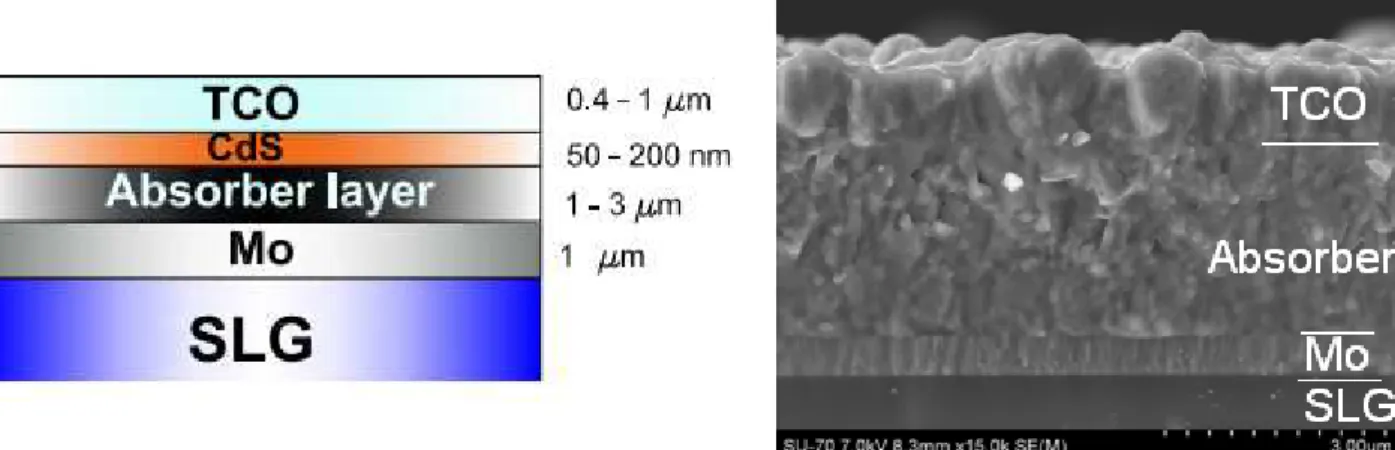
In Figure 1-1, a typical CIS solar cell in the substrate configuration is represented. These cells are usually grown on soda lime glass (SLG) and the back electrode is usually a layer or a bilayer of molybdenum with thickness between 0.5 µm and 1 µm. The absorber layer comes next with a thickness ranging from 1 µm up to 3 µm. To complete the junction an n-type material is required and CdS with a thickness of around 50 nm is used, this layer is called the buffer layer. Atop the buffer layer a window layer is deposited, for this a transparent conductive oxide layer such as aluminium doped - zinc oxide (ZnO:Al), gallium doped zinc oxide (ZnO:Ga) or tin doped indium oxide (ITO) are used. At the top there can be a metallic grid for better charge collection, for this, usually a grid of nickel and aluminium is used, afterwards an anti-reflection layer, generally made of magnesium fluoride, can also be used.
3 In this thesis the chosen nomenclature for CuInSe
1.5 - The availability of indium
Figure 1-1: a) Layer sequence of a thin film solar cell device with the following sequence: SLG/Mo/absorber layer/CdS/TCO. The figure is not to the scale. b) SEM micrograph of a thin film solar cell cross section, the CdS layer is not visible.
This typical solar cell structure was first described in 1985 by Potter et al. [20]. Since then some modifications have been made to improve the efficiency but the structure of the cell is the same and the changes were focused rather on the understanding of the physics of the materials and of the cells.
1.5
The availability of indium
One of the problems that the CIS industry will be facing in the future will be the high prices of indium. Indium is mined as a by-product of Zn [21] and it is quite scarce on the earth’s crust, 0.049 ppm [22, 23]. For comparison, one can see in Figure 1-2 the abundance in the earth's crust and prices for different elements. Because In is so scarce, the demand can be larger than the supply and this leads to high variations in the price.Figure 1-2: Abundance of elements (upper part of the figure) and 2007 prices of raw elemental materials
Green has estimated that in order to keep the contribution of In below 0.20 US$/W in the cost of a solar module, indium prices would have to be lower than 1600 US$/kg [21]. As B. Schubert et al. point out, by dividing the known indium reserves by its current annual consumption, indium will be exhausted within the next 14 years [24]. However, if the same calculation had been done 10 years ago, predictions would indicate that indium would have been completely exhausted by now. Both these statements make us realize that estimating the future prices and availability of a resource and its influence on an industry is a hard task. If one considers the scarcity of indium and assumes that in the near future, CIS will have production plants with capacities of GW/year, it is quite clear that indium will be a limiting factor for reduction of the cost per Watt of a solar module. Some short term solutions for the problem rely on raising the efficiencies of the solar modules or use thinner layers of the absorber material. These actions are already being taken in the industry but will not solve the problem.
Another alternative solution for the indium problem is to replace the absorber layer with a material that does not use scarce elements. Cu2ZnSnSe4 (CZTSe) or Cu2ZnSnS4 (CZTS) are possible options. These materials started to be studied in the late 1980s and 1990s [25-28] but it was in the last decade that they gained more attention. They are both p-type materials and only need a few microns of material in order to absorb almost all the incident light. Moreover their crystalline structure is similar to the CIS one.
1.6
Scope of this thesis
This thesis focuses on two subjects: the optimization of CIGS’s growth by the hybrid method which is the follow up of previous work, and the study of Cu2ZnSnSe4 and Cu2ZnSn(S,Se)4 as possible alternatives as absorber layers for solar cells.
Different approaches for Ga incorporation in CIGS have been studied in this work. Three different setups were analysed: sputtering of Ga using a liquid target, direct evaporation of Ga and the use of a CuGa target.
Regarding CZTSe, different approaches have been addressed during this work as well. At the beginning of these studies, almost no thermodynamic growth data was available for the latter material, therefore a large part of the studies conducted focused on
1.6 - Scope of this thesis
finding the right conditions to grow single phase CZTSe. After the right conditions to grow CZTSe were found, more detailed studies of the properties of this material were possible and solar cells were prepared. In the last part of the thesis, preliminary work on the growth of Cu2ZnSn(S,Se)4 was carried out and some results are shown.
A significant part of the work leading to this thesis aimed at improving the solar cell base-line production of the research group and therefore some work on the other layers was also done. The most important and detailed one was the study of the molybdenum bilayer.
The thesis is divided in 6 chapters. Chapter 1 is the introduction followed by chapter 2 where a review of the state of the art and the properties of CIGS and CZTSe is done. In chapter 3 the experimental techniques used in this work are described and in chapter 4 the growth and properties of the absorber layers are presented. The solar cell results, as well as the optimization studies for the other solar cell layers can be found in chapter 5. Finally, in chapter 6, the conclusions of the thesis are drawn and suggestions for further work are presented.
2
Solar cells and new absorber materials
This chapter is divided into three different sections. The first one is the electrical considerations of p-n junctions and its relation with solar cells. Then follows a section devoted to each material studied in this work. The most important properties of CIGS are presented in section 2.2. There, the objective was not to have a fully detailed description of the material but rather a small introduction since the studies of CIGS are a follow up of previous works. CZTSe is explored in section 2.3 and CZTSSe is the main topic of section 2.4.
Before addressing each of the subsections, let us consider the several requirements for the absorber material used in thin film solar cells. These will allow a better understanding of some of the concepts explained ahead in the text.
In order to obtain the maximum efficiency, the material used as absorber needs to have a band gap energy close to 1.4 eV as stipulated by the Shockley-Queisser limit [29]. This already limits the efficiency of a p-n junction based solar cell to 33%. Basically this constraint comes from the fact that photons with energy lower then the band gap are not absorbed and the ones with higher energy generate hot carriers, losing their energy to increase the absorber temperature.
Electrically, the material should be capable of delivering charge carriers. For that, high diffusion lengths both for electrons and holes are required, but since the films used are polycrystalline, the life time and diffusion length of the carriers are not as high as in mono-crystalline films, this requires the films to be as thin as possible. Having that in mind, the material has to absorb as much incident light as possible, thus having a high absorption coefficient, α, is crucial. For α close to 105 cm-1, 2 µm thick films can absorb most of the incident light.
The material must also form an ohmic contact with the metal used as electrical back contact, and have a suitable band alignment with the n-type material. This will be addressed within each material section.
2.1 - Basics of p-n junctions
2.1
Basics of p-n junctions
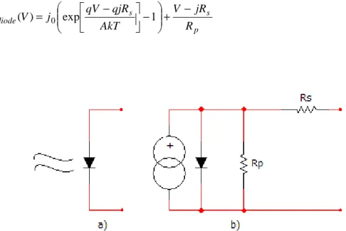
Solar cells are devices based on p-n junctions. Let one consider a p-n+ junction or a diode. The current that flows through a biased p-n+ junction can be calculated using Shockley’s model: − = exp 1 ) ( 0 AkT qV j V jdiode (eq 2-1)
where j is the current density, k the Boltzmann’s constant, T the temperature, V the applied voltage, j0 is a current factor called the saturation current density, q the electron charge and A is the ideality factor for a diode. In a more realistic model than Shockley’s, the losses are
accounted for by including a series, Rs, and a parallel, Rp, or shunt, resistance as presented
in Figure 2-1. Then the current can be described by:
p s s diode R jR V AkT qjR qV j V j + − − − = exp 1 ) ( 0 (eq 2-2)
Figure 2-1: a) Solar cell usual schematic symbol, b) solar cell equivalent circuit.
The exact form of j0 depends on the transport mechanism of the junction. Usually the transport is set by a group of mechanisms rather than by only one. One of the dominant mechanisms that are usually accepted is the diffusion mechanism, there j0 is described by:
− = = kT E qV L N D N qN j j gap D A n V C diif exp 0 (eq 2-3)
where NC and NV are the effective densities of states of the conduction and valence band respectively, NA is the acceptors’ density, LD the diffusion length of electrons and Dn the diffusion constant for electrons in the p-type material.
Under illumination, the electrical properties of the junction are modified because electron-holes pairs are generated and separated by the electric field existing in the depletion region, thus creating a photogenerated current. Electron-hole pairs are also generated outside the depletion region but only the ones at the distance of the diffusion length contribute significantly to the photogenerated current because the others are lost through recombination. The creation of the photogenerated current happens mostly in the absorber layer due to most of the depletion width being located in this layer. Since in thermal equilibrium the electric field far from the junction at either side must be zero, the total negative charge per unit in the p-side must be equal to the total positive charge per unit area in the n-side [30]:
dn d dp
aW N W
N = (eq 2-4)
where Na is the concentration of acceptors in the p-type semiconductor, Wdp the depletion width in the p-type semiconductor, Nd the concentration of donors in the n-type semiconductor and Wdn the depletion width in the n-type semiconductor. Since the p-type material has a higher absorption coefficient than the n-type material, let us consider a p-n+ junction. In this case, Nd will be much greater than Na and therefore, Wdp will be much larger than Wdn. This is why most of the photons that participate in the generation of a photo-current are mostly absorbed in the depletion region of the p-type semiconductor or also called the absorber material. Under illumination, the equation that describes the current of a solar cell is given by:
ph
diode j
j
j= − (eq 2-5)
where jdiode is the current from (eq 2-2) and jph is the photo-generated current. Note that in the situation where Rs=0, Rp= ∞ and V=0, jdiode is zero and then the current that passes
2.2 - CIGS absorber layers
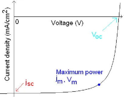
trough the cell is the photogenerated current called short circuit current, jsc. If j=0 the open circuit voltage, Voc, takes the value from (eq 2-7):
sc ph diode j j j =0⇒ = (eq 2-6) + = ln 1 0 j j q AkT VOC ph (eq 2-7)
Another important parameter to evaluate the performance of a solar cell is its conversion efficiency of light to electrical power. This efficiency, η, is the ratio between the maximum produced electrical power, given by jm and Vm, and the incident power, Pinc,:
inc OC SC inc m m P FF V j P V j = = η (eq 2-8)
where FF is the fill factor which describes the area of the j-V curve given by the point
(jm,Vm). High values of fill factor means that the cell may provide more power. FF is given by: OC SC m m V j V j FF= (eq 2-9)
2.2
CIGS absorber layers
CIS is a p-type direct band gap semiconductor and is intrinsically doped since the p-type conductivity comes primarily from Cu vacancies [31]. The compound CuIn 1-xGaxSe2 derives from the chalcopyrite compound CuInSe2 by replacing some of the In by
Ga atoms. CIGS has a high absorption coefficient, around 10-5 cm-1 and a band gap energy that changes with the quantity of Ga present. Since on chemical grounds Ga and In are similar, CIGS has properties close to the ones of CIS. The introduction of Ga into the structure is used because its presence increases the band gap value by changing the minimum of the conduction band. The band gap value of CIS is 1.02 eV and CuGaSe2 has
a band gap value of 1.69 eV. The band gap value of CuIn1-xGaxSe2 where x is
[Ga]/([Ga]+[In]) varies according to the following equation [32]:
( )
x x x x[ ]
eVEgap =1.02+0.67 +0.11 ( −1) (eq 2-10)
Thus band gap engineering is achieved by changing the in-depth Ga concentration. Through this band gap engineering it is possible to enhance the solar cell’s performance.
Usually when growing CIGS, Ga has the tendency to accumulate in the back of the film [33-34]. This, in fact, leads to cells with better efficiencies [35] and the normal explanation for this is due to the formation of a quasi-electric field which leads to reduced recombination at the back contact.
The quasi electric field, ξA, is the effect created by a Ga profile as seen in Figure 2-3. This variation in the concentration of Ga creates a gradient of the electronic affinity since the conduction band is changing and thereby electrons are directed towards the junction [32]. Since Ga content also increases the band gap, it has been found that the maximum solar cell efficiency is obtained when the Ga concentration is increased at the front as well, creating this way a double graded profile as shown in Figure 2-2. This double grading is only considered beneficial if the top grading does not create a bang gap value higher than at the back and if it is inside the depletion width [33]. There is also the possibility of increasing the band gap at the surface of the film, by replacing Se by S which also increases the band gap. CuInS2 is also an interesting material for solar cell
applications, due to its higher band gap energy, but was not studied in this thesis so it is not reviewed here, for more information on this compound the reader can see for instance R. Klenk et al. [36].
Figure 2-2: Double graded profile on band gap of a CIGS film. The left part is the top of the film and the right part is the back. Adapted from [37].
2.2 - CIGS absorber layers
Figure 2-3: Band diagrams of a CIGS thin film solar cell. The dotted line illustrates the effect of increasing the Ga content at the valence band. An additional “electric field” is obtained due to the band gap variation. Adapted from [32].
One of the most important and interesting properties of CIGS is its distinct shift of properties when passing from a Cu-poor phase to a Cu-rich phase. Cu-rich CIGS is formed with large grains and therefore good crystalline properties but its electrical properties are poor to be used in solar cells, mainly because it may grow with n-type conductivity. Cu-poor CIGS films have usually smaller grains and therefore worse crystalline properties but electrically are much more suitable than Cu-rich CIGS [38]. In order to try to use both properties, a bilayer process was first tried by Mickelsen et al. [39]. This process is usually called the Boeing process, and basically consists in growing CIGS using co-evaporation in two steps. The first step is Cu-rich and thereby produces films with large grains, followed by a Cu-poor step where the film reaches the desired stoichiometric point with larger grains and good electrical properties.
Nowadays, the best CIGS thin film solar cells are obtained when the absorber is grown by co-evaporation using a 3-step method. Instead of using the bilayer process, the film is initially grown in a Cu-poor state, then Cu-rich and finally finishes in a Cu-poor state [35, 40-42]. What makes this transition even more interesting is that due to a change in the film’s emissivity, the thermal energy, needed to sustain a certain substrate temperature, changes from one state to another [43, 44]. This makes the in situ
identification of the Cu-poor/Cu-rich transition possible during the growth of the film simply by looking at the substrate temperature or heater power needed during the different steps. This in situ technique to evaluate the Cu-state of the films was firstly used by Kohara et al. [45]. Afterwards several research groups started to call it End Point Detection, or EPD [46, 47]. The change of the film’s emissivity is associated with abrupt change in the hole concentration caused by the Cu vacancies [43].
The author with this section does not intend to make an exhaustive review of the CIGS’s properties but rather an introduction to this type of materials. This is so, mainly because the studies done on CIGS in this thesis were just a small part of the whole work which was focused on CZTSe. Nevertheless, if the reader would like to acquire a more in depth knowledge of CIGS, there are some papers about the properties of CIGS that the author recommends. Theoretically the electronic structure of CIS compounds has been studied by Zunger’s group [31, 48]. Regarding the growth of CIGS, there are at least three good reviews that cover most of the techniques used to grow CIGS, Kemmel et al. [49] and Niki et al. [50]. Non-vacuum methods are explored by Hibberd et al. [51]. CIGS structural properties have been the topic of several review papers [52-55]. The electrical properties with a special focus on the grain boundaries have been reviewed by Siebentritt et al. and Hafemeister et al. [56, 57]. The influence of Na was the topic of study of Rudmann’s PhD thesis [58]. The Ga profile was studied numerous times by several research groups, see for instance [32] and a detail study on the change of emissivity of the films is done in [59].
Since the Ga profile plays a very important role in the solar cells’ performance and is considered a challenge to be used at an industrial scale, in this thesis different incorporations of Ga are tested in the hybrid method. The first one was an attempt of sputtering films of Ga using a target of Ga. The next one was to evaporate Ga and finally the use of a CuGa target to introduce Ga in the films by sputtering.
2.3
CZTSe absorber layers
The idea of using CZTSe as a replacement for CIGS, is the result of an argument for the need to replace In by cheaper elements. Zn and Sn were introduced to replace In and form CZTS for the first time by Ito [25]. CZTSe solar cells were first presented by
2.3 - CZTSe absorber layers
Friedlmeier in her Ph.D. thesis [28]. CZTSe appeared as a good replacement, because there were some reports that showed the material to be p-type and had a high absorption coefficient.
The CZTSe structure is somewhat similar to the CIGS structure. CIGS crystallizes in the chalcopyrite structure which belongs to the tetragonal system. Basically it is a tetragon made of two sphalerite structures on top of each other. This makes a=b and c~2a. The stannite structure is obtained by lowering the symmetry of chalcopyrite and replacing the element of group III by two of groups II and IV. This decrease of symmetry is obtained by the substitution of the metals, but also by changing the metal ordering, i.e. the arrangement of the cations on the structural sites of the unit cell. The kesterite structure is obtained by further changing the order of the cations. These modifications can be seen in Figure 2-4.
The names of these structures come from the mineral names, kesterite is Cu2ZnSnS4 and stannite is Cu2FeSnS4. The mineral kesterite was first mentioned in the
literature in 1958 by Orlova [61]. As stated before, both structures are derived from the chalcopyrite structure, mineral CuFeS2. The family of all these compounds is called
adamantine. These materials were studied by Pamplin [62] where he first described that these materials should obey the octet rule, i.e., there should always be eight electrons around each chalcogen atom.
The difference between stannite and kesterite is seen in Figure 2-5 and in Table 2-1. The CIS chalcopyrite structure is represented in Figure 2-5 as well. The difference of the two structures relies on a switch of positions between Cu and Zn, being the kesterite structure more disordered. The ions Cu+ and Zn2+ have the same number of electrons and these elements are neighbours in the periodic table. Their atomic scattering factor, which is proportional to the measured intensity in an X-ray diffraction experiment, is identical. Hence these ions are not distinguishable by conventional X-ray diffraction (XRD). Schorr [60] has suggested using neutron diffraction as a possible technique to distinguish between stannite and kesterite.
Figure 2-5: Crystal structure of chalcopyrite, kesterite and stannite. Highlighted in red, the differences in the Zn and Cu atoms are shown. Adapted from [54, 63].
2.3 - CZTSe absorber layers
Table 2-1: Position of atoms for the stannite and kesterite structures. I-42m
Stannite I-4 kesterite Position Wyckoff / atom Wyckoff / atom (0,0,0) 2a Zn2+ 2a Cu1+ (½,½,0) 2b Sn4+ 2b Sn4+ (0, ½, ¼) 4d Cu1+ 2d Cu1+ ( 0, ½ , 3/4) - 2c Zn2+ (x,x,z) 8i Se2- - (x,y,z) - 8g Se
2-Despite this identification problem, several studies assign CZTSe to the stannite structure as is shown in the historical overview of Table 2-2. This historical overview shows that regardless of the identification problem, several research groups stated that the structure is stannite. This probably happened in a cascade process where the first author stated to have the stannite structure. After that and since the position of the peaks for stannite and for kesterite are exactly the same, other research groups followed the same interpretation. To complicate even further the problem, in the International Centre for Diffraction Data, there is only a datasheet for stannite CZTSe. Later in this thesis, this identification problem will be addressed.
Table 2-2: CZTSe structural identification reported.
Year Reference a c c/2a Structure
1965 64 5.681 11.34 0.998 stannite 1974 65 5.681 11.34 0.998 stannite 1979 62 5.69 - - sphalerite 1980 66 5.681 10.843 0.954 stannite 1997 28 - - - kesterite 2000 67 5.693 11.333 0.995 stannite 2002 68 5.689 11.337 0.996 stannite 2005 69 5.597 11.21639 1.002 stannite 2005 70 5.693 11.33 0.995 ? 2006 71 - - - stannite 2007 72 5.776 11.677 1.011 stannite 2008 73 5.68 11.36 1.000 kesterite 2008 74 5.69 11.41 1.003 kesterite 2009 75 5.684 11.353 0.999 stannite
The growth of CZTSe thin films has been firstly reported by Pamplin et al. [62]. Guen et al. [66] reported the growth of CZTSe by iodine transport with the objective to study electrical and magnetic properties. After this early work, only Friedlmeier [28] in 1997 presented results on the growth of CZTSe solar cells grown by co-evaporation with an efficiency of 0.6%. Although it was never calculated directly, Friedlmeier estimated the band gap energy to be around 1 eV. Matsushita [67] grew CZTSe crystals and obtained samples with a p-type conductivity, a band gap energy of 1.44 eV and a melting point around 805 ºC. Olekseyuk [68] studied single crystals and reported Ritveld analysis proving that the crystallization of CZTSe was done in the stannite structure. The first and only thermodynamic study of the CZTSe phase equilibria was done by Dudchak in 2003 [76]. Using ab-initio calculations Raulot [69] estimated the band gap energy of CZTSe around 0.9 eV. Matsushita [70] estimated the band gap energy of CZTSe single crystals to be 1.5 eV. In 2006 Altosaar [71] reported preparation of CZTSe monograins solar cells. In the latter they show different studies and properties: a photoluminescence emission at 0.81 eV; a XRD diffractogram in which the stannite structure was presented; express doubts over the band gap energy which is as high as 1.5 eV and present solar cells with an efficiency of 1.8%. Wibowo et al. [72] presented the growth of CZTSe thin films by RF magnetron sputtering from binary chalcogenide targets at a substrate temperature of 175 ºC, then they show a XRD diffractogram with 5 reflections. In that work a band gap energy of 1.56 eV was also reported. In 2007 Wibowo et al. [77] have also grown CZTSe thin films by selenization of sputtered binary compounds, it was basically an annealing of the samples grown in the previous report. Still in 2007, Wibowo et al. [78] reported the growth of CZTSe thin films by pulsed laser deposition of a quaternary target. In that work, the best films were grown at a substrate temperature of 500 ºC and the following properties were calculated: band gap energy of 1.5 eV, a free carrier density of 2.2 x 1017 cm-3 and a Hall mobility of 1.5 cm2V-1s-1. In 2007 Herbert et al. [79] predicted that there are two paths for the formation of CZTSe:
Path 1 Cu2Se/CuSe + ZnSe + SnSe/SnSe2 (+/-Se) → CZTSe Path2: a) Cu2Se/CuSe + SnSe/SnSe2 → Cu2SnSe3
2.3 - CZTSe absorber layers
Later in this thesis, it will be shown that it is likely that in some cases, both paths happen at the same time. Babu et al. [73] grew CZTSe thin films by co-evaporation and estimated that the best growth temperature under those conditions was 350 ºC without an annealing step, and 450 ºC with an annealing step. They obtained XRD peaks as broad as 0.3º and by looking at the (1 1 2) peak they were able to identify CZTSe and ZnSe. A band gap energy of 1.48 eV and an optical absorption coefficient higher than 105 cm-1 were reported. The same results were presented by Babu et al. in another paper [74]. In 2008 Altosaar [80] revealed for the first time Raman scattering studies of CZTSe. They identified the peaks at 173 cm-1, 196 cm-1 and 231 cm-1 as CZTSe Raman scattering peaks. In the same work, the authors saw a PL emission at 0.85 eV and presented solar cells based in mono-grains with an efficiency of 2.16 %.
With the record efficiency of a CZTS solar cell of 6.7 % reported by Katagiri et al. in 2008 [81], the whole family of materials, CZTS and CZTSe, started to attract more attention from the research community. In 2009 the number of papers with the main topic being CZTSe suddenly increased.
The photoluminescence emission from CZTSe monograins was studied by Grossberg et al. [82] in 2009 and a broad emission at 0.946 eV was found for the CZTSe. With these experiments, they estimated the band gap energy of CZTSe to be around 1.02 eV. Volobujeva et al. [83, 84] presented in 2009 CZTSe thin films grown by selenization of metallic evaporated precursors. In the same work the authors showed Raman and XRD studies and only obtained good quality CZTSe films at temperatures higher than 370 ºC but were not able to grow single phase films. Wahab et al. [85] studied CZTSe films grown by the melt quenching technique. They showed very poor quality films with a band gap energy of 1.7 eV. In 2009 Zoppi et al. [75] reported an efficiency of 3.2 % for a CZTSe solar cell grown by selenization of metallic precursors deposited by magnetron sputtering. They estimated the band gap energy to be 0.94 eV using the external quantum efficiency. Until the date of writing of this thesis, this is still the best reported efficiency for solar cells using CZTSe thin films. The electronic structure of CZTSe was studied using first principles calculations by Nakamura et al. [86], they reported a band gap energy of 1.7 x 10⁻⁵ eV. Liu et al. [51] grew slightly Cu-rich CZTSe crystals to study its thermoelectric properties. Shi et al. [87] analysed CZTSe ingots and reported the following parameters: electrical conductivity of 4500 Sm-1; a Seebeck coefficient of 130 µVK-1, a thermal
conductivity of 3.2 Wm-1K-1 and a hole concentration of 1 x 1019cm-3. An additional possible structure has been suggested to appear in CZTSe by Chen [88]. They have suggested that not only kesterite (KS), I-4, and stannite (ST), I-42m, could appear but a primitive mixed CuAu-like (PCMA), P-42m was also possible. They have estimated, by first principles calculations, that KS is the most stable structure because of its lowest formation energy value, however the difference to ST is only 3 meV. To complicate even more, the same research group suggested another structure, a partially disordered KS (PD-KS). They estimated the band gap energy to be 0.96 eV and despite all these phases, the ordering of the Cu and Zn atoms should not influence strongly the electrical properties since the band structure barely changes. Using density functional theory, Sevik et al. [89] stated that the density of states and band structures of the different possible structures, KS, ST and PCMA, is so similar that no changes in the structure, mechanical and electronic properties should be seen. Chen et al. presented two different papers [90, 91] where the results for the properties of CZTSe and other materials were calculated by density-functional theory. Their main conclusions were: kesterite has a value of c/2a lower than 1 and it is the most likely structure, the reported stannite structure in the literature is probably a partially disordered KS, the band gap energy was estimated to be 1.0 eV for the kesterite and there should not be a difference larger than +0.2 eV in the band gap energy for the stannite structure.
In 2010 a high number of publications with CZTSe as the main topic continued to appear. CZTSe nanocrystals were chemically deposited by Shavel et al. [92]. Krustok et al. [93] found a value for the band gap energy of 1.0 eV by analysing the quantum efficiency curves on CZTSe monograin solar cells and estimated that the material had spatial potential fluctuations with an average depth of 25 meV. Todorov et al. [94] announced a new record for kesterite based solar cells grown using a non vacuum ink process. He presented a solar cell with a conversion efficiency of 9.66% with an absorber layer consisting of Cu2ZnSn(S,Se)4 (CZTSSe). It is expectable that this value, which is close to
10%, will bring even more research groups into the area. Krustok et al. [95] continued the analysis of monograin CZTSe solar cells and reported a degradation of the Voc with
temperature of -1.97 mV/K. Babu et al. [96] continued to grow CZTSe thin films by co-evaporation and presenting XRD diffractograms showing films with broad peaks. The latter authors estimated a band gap energy ranging between 1.37 eV and 1.62 eV for
2.3 - CZTSe absorber layers
samples with a ratio [Cu]/([Zn]+[Sn]) of 1.14 to 0.83, respectively. CZTSe nanocrystals formed by hot injection were presented by Hao Wei et al. [97]. The first interesting theoretical in-depth study of CZTSe and CZTS was done by Person et al. [98]. Their main conclusions were: both structures have similar electronic band structure, dielectric functions and optical absorption coefficients; from the possible different structures, kesterite structure is the most likely because of the lower internal energy; the band gap for the kesterite was calculated to be 0.89 eV and for the stannite 1.05 eV; the dielectric constant is between 8.2 and 9.0 and the effective masses of holes and electrons were estimated. Very recently, Ahn et al. [99] using a different method has reported the band gap value of CZTSe to be between 1.02 eV and 1.05 eV which is in accordance with the findings of this thesis. In the same work they used not only XRD but also Raman scattering to confirm the presence of CZTSe.
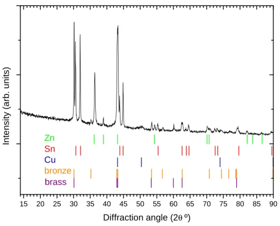
2.3.1 Phase identification problem with XRD
A problem that is usually overlooked in the publications where CZTSe is addressed is its XRD peak assignment. Resolving CZTSe from unwanted secondary phases is difficult using XRD data. In Table 2-3 the unit cell sizes for CZTSe, cubic ZnSe, cubic Cu2SnSe3 and cubic Cu2Se, are presented and one can see they are almost the same. Other
phases, namely CuSe, SnSe and Sn2Se are also presented, but these can be identified using
XRD analysis. The biggest difference is for Cu2Se which can be resolved using XRD. The
difference in the lattice parameter a, is less than 0.004 Å for the cubic Cu2SnSe3 and less
than 0.02 Å for ZnSe. Given that CZTSe has the stannite or the kesterite structure that comes from the tetragonal family which is basically a double-cubic structure, most of its reflections are in the same position as the above mentioned phases. This is seen in Table 2-4 where the most intense peaks for these phases are presented. There is also a row where the angular differences between the position of the unwanted phases and the position of CZTSe are shown. For ZnSe, the largest difference is 0.15º. For CZTSe the peak is situated at 72.48 º with an intensity of 76, whereas the ZnSe peak is situated at 72.63º with intensity 331. Note that these intensities are normalized to 1000, which means that these peaks are quite weak. Usual system resolutions for XRD systems are close to these angular differences. With broad peaks, this distinction is even harder to detect. For the cubic
Cu2SnSe3, the biggest difference is 0.16º. The two presented copper-selenide phases are
easier to identify since the differences to CZTSe are bigger than the previous compounds. For the cubic and for the hexagonal phase the peak positions are quite dissimilar as they have different structures. Despite the fact that all the cubic ZnSe and cubic Cu2SnSe3
diffractions peaks are extremely close and/or superimposed with those of CZTSe, the latter possesses additional peaks that are not common with these unwanted phases. Such examples are the peaks at 15.61º and 17.42º and the double peaks at 53º, 65º and 72º. Usually, the intensity of the single peaks and the double peaks at 65º and 72º is low and therefore the double peaks at 53.39º and 53.53º can be used to evaluate the presence or absence of CZTSe. Using these peaks, one can then say whether CZTSe is present or not. However, nothing can be said regarding the other phases. Most of the works reported before, only use XRD to evaluate the presence of secondary phases and so, the author believes that some of the presented properties, supposedly belonging to CZTSe, may be, in reality, the effect of unwanted phases. Such example is the band gap energy, for which until 2010 there were reports for values ranging from 1.0 eV to 1.5 eV. As reference, the band gap energies for CZTSe and other phases likely to appear during its growth are presented in Table 2-3 .
In order to overcome the identification problem, the author has suggested the use of Raman scattering as a complementary technique to analyse the different phases present [I]. Raman scattering can provide phase identification and in well studied materials can be used to assess nano-scale structural changes. For more information on Raman scattering the review paper of Gouadec is recommended [101].
2.3 - CZTSe absorber layers
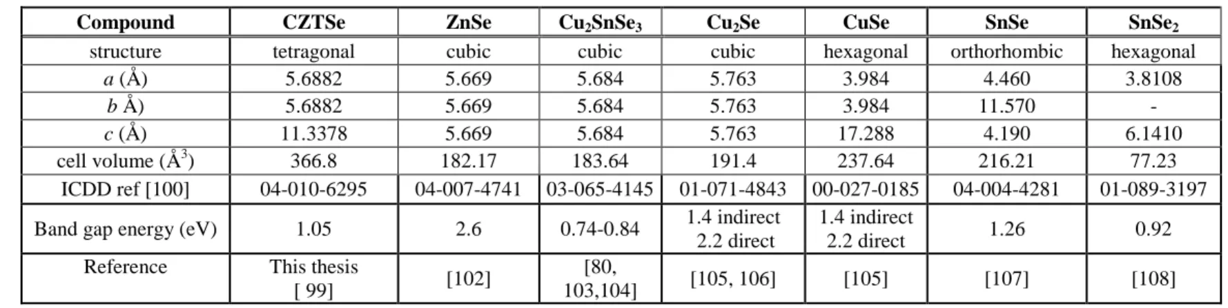
Table 2-3: Unit cell properties: differences between CZTSe, ZnSe, CTSe, Cu2Se and CuSe.
Table 2-4: XRD peak positions for different selenide compounds [100].
Compound CZTSe ZnSe Cu2SnSe3 Cu2Se CuSe SnSe SnSe2
structure tetragonal cubic cubic cubic hexagonal orthorhombic hexagonal
a (Å) 5.6882 5.669 5.684 5.763 3.984 4.460 3.8108
b Å) 5.6882 5.669 5.684 5.763 3.984 11.570 -
c (Å) 11.3378 5.669 5.684 5.763 17.288 4.190 6.1410
cell volume (Å3) 366.8 182.17 183.64 191.4 237.64 216.21 77.23
ICDD ref [100] 04-010-6295 04-007-4741 03-065-4145 01-071-4843 00-027-0185 04-004-4281 01-089-3197 Band gap energy (eV) 1.05 2.6 0.74-0.84 1.4 indirect
2.2 direct
1.4 indirect
2.2 direct 1.26 0.92 Reference This thesis
[ 99] [102] [80, 103,104] [105, 106] [105] [107] [108] CZTSe angle (º) Intensity (arb. units) Planes ZnSe angle (º) Intensity (arb. units) Planes Difference to CZTSe (º) Cu2SnSe3 angle (º) Intensity (arb. units) Planes Difference to CZTSe (º) Cu2Se angle (º) Intensity (arb. units) Planes Difference to CZTSe (º) 27.16 999 112 27.22 999 111 -0.06 27.15 999 111 0.01 26.88 473 111 0.28 45.12 493 204 45.2 585 220 -0.08 45.07 597 220 0.05 44.61 999 220 0.51 53.39 230 312 - - - - 53.53 233 116 53.57 315 311 -0.04 53.41 321 311 0.12 52.86 152 311 0.67 65.59 52 400 - - - - 65.84 34 8 65.84 70 400 0 65.64 71 440 0.2 64.92 117 400 0.92 72.36 42 332 - - - - 72.48 76 316 72.63 94 331 -0.15 72.41 96 331 0.07 - - - - 83.19 87 424 - - - - 83.35 57 406 83.46 110 422 -0.11 83.19 113 422 0.16 82.2 180 422 1.15
2.3.2 Phase diagrams, band diagrams and electrical properties
For the CZTSe system there is a work done by Dudchak et al. [76] that covers most of the binary and ternary combinations of Cu-Sn-Zn-Se phases. Among many results, the most significant one showed that there was low solubility of CZTSe with binaries and the composition intervals where it is formed are narrow. This shows that the formation of non-stoichiometric CZTSe is hard, if not almost impossible.
Regarding the electrical properties, for CZTSe there is not yet a detailed study, but there is a theoretical one made by Chen et al. [109] for CZTS. CZTS and CZTSe should have some similarities in the electronic structure and therefore it is relevant to take a look at those studies. Chen et al. reported that the dominant p-type defect is CuZn with an
acceptor level higher than the one for the chalcopyrites, which suggests that p-type doping in CZTS is more difficult than other chalcogenide compounds such as CuInSe2. They
propose the growth of CZTS in Cu-poor/Zn-rich conditions, and thus VCu and ZnCu should
become the dominant defects in the system since its formation energies are lower, however this condition may lead to the formation of unwanted phases like ZnS. Similar studies for CZTSe are needed to understand if the underlying physics is the same or not. It is necessary to correlate that future information with the one provided by Dudchak et al. [76] to evaluate if the intrinsic doping of single phased CZTSe is possible and under what conditions.
There are still a considerable number of problems dealing with the growth of the CZTSe absorber and thereby the optimization or even the study itself of the solar cell structure is something that has not yet been done. Thus, the best solar cells made with an absorber layer of CZTSe, CZTS or even CZT(S,Se) are still made with the structure: SLG/Mo/CZTS/CdS/i-ZnO/ZnO:Al, which has been optimized for CIGS.
The problem of finding the right conditions for the growth of the absorber bring severe problems to the optimization of cells since the absorber layer’s properties are unknown and hence there is less freedom to explore different approaches to the cell structure. In order to start grasping the band diagram of the actual structure, some of the chalcogenides properties need to be known: band gap energy, electron affinity, the Fermi energy level, carrier concentrations, effective masses for electrons and holes, density of states and the work function. Some experimental measurements like X-ray photoelectron

![Figure 4-8: Composition ratio, [Cu]/([Sn]+[Zn]), estimated by ICP-MS versus the thickness ratio, Cu/(Sn+Zn)](https://thumb-eu.123doks.com/thumbv2/123dok_br/15910145.1092548/75.892.198.677.349.719/figure-composition-ratio-estimated-icp-versus-thickness-ratio.webp)