Eduardo Manuel Ribeiro Duarte
Licenciado em Ciências de Engenharia FísicaLow-Cost Thin Film Perovskite Solar Cells
Dissertação para obtenção do Grau de Mestre em
Engenharia Física
Orientador: Manuel João de Moura Dias Mendes, Post-Doc Fel-low, FCT-UNL
Co-orientadora: Elvira Maria Correia Fortunato, Full Professor, FCT-UNL
Júri
Presidente: Professora Doutora Isabel Catarino, FCT, UNL Arguente: Doutora Alexandra Barreiros, LNEG
Low-Cost Thin Film Perovskite Solar Cells
Copyright © Eduardo Manuel Ribeiro Duarte, Faculdade de Ciências e Tecnologia, Uni-versidade NOVA de Lisboa.
A Faculdade de Ciências e Tecnologia e a Universidade NOVA de Lisboa têm o direito, perpétuo e sem limites geográficos, de arquivar e publicar esta dissertação através de exemplares impressos reproduzidos em papel ou de forma digital, ou por qualquer outro meio conhecido ou que venha a ser inventado, e de a divulgar através de repositórios científicos e de admitir a sua cópia e distribuição com objetivos educacionais ou de inves-tigação, não comerciais, desde que seja dado crédito ao autor e editor.
A c k n o w l e d g e m e n t s
Gostaria de agradecer em primeiro lugar à Prof. Dra. Elvira Fortunato e ao Prof. Dr. Rodrigo Martins, que continuam a proporcionar a tantos alunos, os recursos para que estes possam perseguir os seus sonhos académicos. Um agradecimento especial aos meus orientadores, Prof. Elvira Fortunato e Prof. Manuel Mendes pela oportunidade de trabal-har e explorar um tema interessante e importante para a nossa sociedade, e pelo apoio prestado ao longo deste trabalho.
Um grande agradecimento vai também para a mestre Carolina Fidalgo por me ter at-urado em momentos de desespero e pelos conselhos de um Perovskito para outro. Outro grande agradecimento vai também para o mestre Alexandre Fonseca por me mostrar muito do que apliquei e me aconselhar e aturar muito depois do seu trabalho estar con-cluído. Quero deixar igualmente o meu agradecimento à Beatriz Esteves pela sua valiosa ajuda na fabricação de muitos dos dispositivos deste trabalho. A special English thank you goes to Deneb, for advising me and helping me in the beginning of my thesis, when I was feeling lost the most.
Quero agradecer à equipa do Cenimat: Alexandra Gonçalves, Sónia Pereira, Rita Branquinho, Joana Pinto, Andreia Araújo, Carolina Marques, Sofia Ferreira, Emanuel Carlos, Olalla Sanchez e Daniela Gomes, por toda a paciência que tiveram comigo e pela sua ajuda e competência em tarefas que em muito contribuíram para o trabalho desta tese.
Quero agradecer a todos a quem me orgulho de chamar amigos, alguns de longa data, outros adquiridos neste precurso académico, mas todos estes deixaram a sua marca e que me ajudaram a chegar onde estou hoje. A todos voçês um muito obrigado do fundo do coração por todos os momentos e que seja até aos 100!
Um agradecimento especial vai também para a Vó Sofia por todo o apoio e paciência na nossa convivência de avó e neto. Um enorme Obrigado terá claro de ir para os meus pais, Cristina Duarte e Francisco Duarte, de que tanto me orgulho e que sei que sempre deram e sempre darão tudo por mim, com apoio incondicional nas melhores e piores alturas.
A b s t r a c t
Perovskite is a class of materials named after their characteristic crystal structure, present-ing excellent optoelectronic properties. These properties (particularly, ambipolar charge transport) allow these materials to integrate solar cells with and without the addition of selective layers, like Electron-Transport-Layer and Hole-Transport-Layer, possessing also the ability to be fabricated using simple, non-expensive, solution processing techniques, like Spin-Coating. Coupled with its facile production, the steep rise in SC efficiency
over the last years, makes these materials a strong candidate to replace Silicon in the photovoltaic market, both in solid-state and flexible devices.
Despite its many advantages, Perovskite SC still face considerable costs regarding processing conditions and HTL materials. By fabricating these devices under ambient air conditions and using Copper(I) Thiocyanate as the material for the HTL, the fabrication costs are significantly reduced. To further lower fabrication cost, Methylammonium Chloride is studied as a replacement for Methylammonium Iodide in Perovskite precursor solution fabrication. Using this solution, crystalline films were obtained, studying several deposition parameters, and the best reported ones, should provide a starting point for further optimization under similar fabrication conditions.
The main goal for this work was the optimization of SC, using Spin-Coating tech-nique, keeping the devices as low-cost as possible. Improving Perovskite film quality is detrimental to enhance SC performance, which is why efforts were made to minimize
film degradation during Perovskite film fabrication and HTL deposition steps.
Due to the hygroscopic nature of the organic component in Perovskite films, the influence of humidity levels was tested, and methods to reduce thin film degradation via humidity exposure were also evaluated.
Overall, device optimization was successful, with Perovskite films reaching >95% bulk density and the champion device presenting PCE of 2.65%, with Jscof 15.11 mA/cm2 and Vocof 0.701V.
R e s u m o
A Perovskite é uma classe de materiais assim denominada devido à sua estrutura crista-lina, possuindo excelentes propriedades optoeletrónicas. Estas propriedades (em especial, transporte ambipolar) permitem que estes materiais sejam aplicados em células solares, com e sem a adição de camadas, comoHole-Transport-LayereElectron-Transport-Layer. A
possibilidade de serem fabricadas através de técnicas simples e de baixo custo, aliado à rá-pida subida na eficiência destes dispositivos nos últimos anos, faz da Perovskite uma forte candidata a substituir o Silício, tanto em dispositivos de estado-sólido, como flexíveis.
Apesar das vantagens, estes dispositivos enfrentam elevados custos de produção de-vido não só ao seu processamento, mas também à escolha de materiais, em particular para aHole-Transport-Layer. A fabricação destas células em condições atmosféricas nor-mais, através de Spi-coating e usando Tiocianato de Cobre como material para a HTL, torna os custos de produção significativamente reduzidos. No entanto, de forma a reduzir ainda mais o custo, foi estudado Cloreto de Metilamónio como substítuto para o Iodeto de Metilamónio na fabricação da solução precursora de Perovskite, uma vez que este é significativamente menos dispendioso. Embora não tenha sido possível obter dispositivos altamente eficientes, obtiveram-se filmes cristalinos, usando esta solução.
O principal objetivo deste trabalho consistiu na otimização de células solares, man-tendo um reduzido custo de fabricação. Melhorar a qualidade da Perovskite é essencial para aumentar a eficiência, tendo sido por isso feitos esforços para minimizar a degrada-ção da camada ativa, durante a fabricadegrada-ção do filme de Perovskite e deposidegrada-ção da HTL.
Devido à natureza higroscópica da componente orgânica da Perovskite, foi testada a influência da humidade na formação de filmes, bem como também diferentes métodos para reduzir a degradação do filme devido à exposição à humidade.
Com base nos diferentes testes, a otimização dos dispositivos solares foi bem suce-dida, obtendo-se filmes de Perovskite com densidades em volume superiores a 95%, uma eficiência de 2,65%, Jsc de 15,11 mA/cm2e um Voc de 0,701 V para o melhor dispositivo.
C o n t e n t s
List of Figures xv
List of Tables xxi
Acronyms xxiii
1 Goals and motivation 1
2 Introduction 3
2.1 Solar Cell . . . 4
2.2 Perovskite Materials . . . 5
2.2.1 Crystalline Structure . . . 6
2.2.2 Perovskite - Thin Film fabrication. . . 7
2.3 Electron and Hole Transport Layers . . . 9
2.3.1 Electron Transport Layer - ETL . . . 10
2.3.2 Hole Transport Layer - HTL . . . 10
2.4 Film deposition techniques . . . 10
2.4.1 Spin-coating technique . . . 11
2.4.2 Electron-beam evaporation technique . . . 11
2.5 Characterization Techniques . . . 12
2.5.1 SEM - Scanning Electron Microscopy . . . 12
2.5.2 XRD - X-Ray Diffraction . . . 12
2.5.3 Ultraviolet-Visible Spectroscopy. . . 14
3 Experimental Procedure 15 3.1 Substrate Preparation . . . 15
3.2 Film deposition . . . 17
3.2.1 ETL deposition . . . 17
3.2.2 Perovskite deposition . . . 18
3.2.3 HTL deposition . . . 18
3.3 Contact deposition . . . 19
3.4 Characterization . . . 19
3.4.2 UV-Vis Spectroscopy . . . 20
3.4.3 XRD analysis . . . 20
3.4.4 Electrical characterization . . . 20
4 Results and Discussion 21 4.1 Solar Cell Contacts . . . 21
4.1.1 Etching-Method Contacts . . . 22
4.1.2 Perimeter-Mask-Method Contacts . . . 28
4.1.3 Conclusions . . . 31
4.2 MACl as replacement for MAI in Perovskite precursor solution . . . 32
4.2.1 First batch of SC using MACl as a Perovskite solution precursor . 32 4.2.2 Perovskite solvent variation . . . 33
4.2.3 Second attempt at SC fabrication using MACl solution . . . 34
4.2.4 TiCl4as a precursor for the TiO2solution . . . 36
4.2.5 Solvent ratio variation and anti-solvent test . . . 38
4.2.6 Perovskite solution concentration variation . . . 40
4.2.7 Conclusions . . . 45
4.3 Optimization of SC devices . . . 45
4.3.1 Concentration and Annealing time . . . 45
4.3.2 TiO2Mesoporous layer . . . 48
4.3.3 CuSCN as HTL . . . 52
4.3.4 Diethyl Ether as an anti-solvent agent . . . 54
4.3.5 Improving Fill Factor . . . 58
4.3.6 Humidity Influence on device performance . . . 58
4.3.7 Conclusions . . . 65
5 Conclusions and Future work 67
Bibliography 71
A Solar Cell Performance 79
B Materials and solution preparation 83
L i s t o f F i g u r e s
2.1 General working principle of a solar cell [14]. . . 4
2.2 Different Solar Cell arquitectures [15]. a) Planar Structure; b) Inverted
Struc-ture; c) Mesoscopic Structure. . . 5
2.3 Perovskite Crystal Structure; a)Perovskite unit cell [17]; b) Crystal Structure
of cubic metal halide Perovskite (ABX3) [18]. . . 6
2.4 Energy level alignment for some of the materials used in this work; Schematic
band-bending of energy levels [37–40] . . . 9
2.5 Schematic of film fabrication via Spin-coating method [47]. . . 11
2.6 Schematic thin film deposition via E-beam technique [48]. . . 12
2.7 a) Electron-Sample interaction schematic; b) Electron-Sample interaction
vol-ume [51]. . . 13
2.8 Constructive interference of reflected waves according to Bragg’s Law [53]. . 14
3.1 Schematic representation of the SC fabrication process and I-V measurement. 16
3.2 Glass substrate after FTO removal - In grey: un-etched FTO film; In blue:
etched areas(glass only). . . 17
3.3 a) Masks used in the original version of the contacts (opening for contacts:
8x0.6 mm2); b) Masks used for the new contact version (opening for contacts:
10x1 mm2).. . . 19
3.4 a) SC device using original contact version; b) SC device using etching/perimeter-mask version; c) SC device using final version; In white are the areas that re-main film-free; In grayish-blue FTO-only areas; In dark-brown is represented
the effective device area (area where all the layers are deposited; In gold are
represented the different deposited contacts.. . . . 20
4.1 Substrate resulting from the etching method, prior to gold contact deposition, with dimensions as the ones in figure 3.2. Blue color refers to film-free areas of the substrate; Grey color refers to the FTO front contacts; Dark-brown color refers to effective device area. . . 22
4.2 Effects of the Etching contact method on film quality, presenting degradation
4.3 I-V a) and P-V b) measurements for solar devices differentiating on the contact
type (Etching vs Original). Devices fabricated using a compact TiO2 using
TTIP Solution; Perovskite layer using 1 M Solution (MAI:PbI21:1), with 100 µl
chlorobenzene droping, annealed for 60 mins at 100°; CuSCN layer annealed
at 90° for 30 mins. . . 24
4.4 I-V a) and P-V b) measures for SC devices differentiating on contact type
(Etch-ing vs Original - second attempt). Devices fabricated us(Etch-ing a compact TiO2
using TTIP Solution; Perovskite layer using 1 M Solution (MAI:PbI21:1), with
100 µl chlorobenzene droping, annealed for 60 minutes at 100° C; CuSCN
layer annealed at 90° C for 30 minutes. . . 25
4.5 Surface morphology influence with contact type. a) Original-Method; b)
Etching-Method . . . 27
4.6 Difference between devices using the etching-method (on the left) and the
original contact process (on the right). . . 27
4.7 XRD diffractograms - Contact Study: Etching-Method vs Original Method.
Peaks corresponding to the tetragonal phase of MAPbI3, marked with full
rhombus, the PbI2peak, marked with an asterisk and also peaks regarding the
CuSCN and FTO layer (marked with cardinal and full circle, respectively). . 28
4.8 Substrate resulting from Perimeter-Mask Contact Method of fabrication.
Dark-brown area is the effective device area; Gold color area represents the Kapton
mask placed on the substrates before ETL deposition, with the same
dimen-sions as in figure 3.2. . . 29
4.9 I-V a) and P-V b) measurements for SC devices differentiating on contact type
(Perimeter-Mask vs Original).Devices fabricated using a compact TiO2using
TTIP Solution; Perovskite layer using 1 M Solution (MAI:PbI21:1), with 100
µl chlorobenzene droping, annealed for 60 minutes at 100° C; CuSCN layer
annealed at 90° C for 30 minutes. . . 30
4.10 XRD diffractograms - Perimeter-Mask-Method vs Original Method. Peaks
cor-responding to the tetragonal phase of MAPbI3, marked with full rhombus, the
PbI2peak, marked with an asterisk and also peaks regarding the CuSCN and
FTO layer (marked with cardinal and full circle, respectively) . . . 31
4.11 Substrates with compact TiO2and Perovskite layer using 0.217 M MACl
so-lution in DMF. The difference in color tone is most likely related to small
differences in the anti-solvent dropping step such as timing, distance to the
substrate, or disperse flow. . . 32
4.12 Perovskite layer, from different solutions, deposited over glass - a) pure DMF;
b) pure DMSO; c) DMF:DMSO (1:1). . . 33
4.13 I-V a) and P-V b) measurements for SC devices using MACl solution. Devices
fabricated using a compact TiO2using TTIP Solution; Perovskite layer using
0.642 M Solution (MACl:PbI21:1), with 80 µl toluene droping, annealed for
L i s t o f F i g u r e s
4.14 I-V a) and P-V b) measurements for SC devices using MACl solution.
De-vices fabricated using a compact TiO2using TTIP solution or TiCl4solution;
Perovskite layer using 0.642 M Solution (MACl:PbI21:1), with 80 µl toluene
droping, annealed for 10 minutes at 100° C; CuSCN layer annealed at 90° C
for 30 minutes. . . 37
4.15 Topological SEM images: influence of different TiO2 precursor solutions on
perovskite film morphology. a) and b) images refer to a sample prepared using TTIP solution for the ETL layer, while c) and d) images refer to a sample
prepared using TiCl4solution for the ETL. . . 38
4.16 Film variation when using toluene(3 left samples) and chlorobenzene (3 right
samples) as anti-solvent agents. Perovskite film using a 0.642 M MACl:PbI2in
1:1 DMF:DMSO solution with 80 µl droping of anti-solvent agent, deposited over c-TiO2. . . 39
4.17 Perovskite film using a 0.642M in a 1:1 DMF:DMSO ratio precursor solution
with 80 µl of anti-solvent agent, deposited over compact TiO2. a) and b) refer
to the sample with 80 µl of toluene; c) and d) refer to the sample with 80 µl of
chlorobenzene. . . 40
4.18 Perovskite film using a 0.642M in a 2:1 DMF:DMSO ratio precursor solution
with 80 µl of anti-solvent agent, deposited over compact TiO2. a) and b) refer
to the sample with 80 µl of toluene; c) and d) refer to the sample with 80 µl of
chlorobenzene. . . 41
4.19 Perovskite film using a 0.642 M in a 1:2 DMF:DMSO ratio precursor solution
with 80 µl of anti-solvent agent, deposited over compact TiO2. a) and b) refer
to the sample with 80 µl of toluene; c) and d) refer to the sample with 80 µl of
chlorobenzene. . . 42
4.20 Perovskite film using a 0.642 M in a 2:1 DMF:DMSO ratio precursor solution
with 80 µl of chlorobenzene, deposited over compact TiO2. . . 42
4.21 Perovskite film using a 0.868 M in a 2:1 DMF:DMSO ratio precursor solution
with 80 µl of chlorobenzene, deposited over compact TiO2. . . 43
4.22 Perovskite film using a 1.085 M in a 2:1 DMF:DMSO ratio precursor solution
with 80 µl of chlorobenzene, deposited over compact TiO2. . . 43
4.23 XRD diffractograms of samples of fabricated using 3 Perovskite solutions
with different concentrations. Peaks corresponding to the tetragonal phase
of MAPbI3, marked with full rhombus, MApBCl3peaks marked with empty
rhombus, the PbI2 peak, marked with an asterisk and also peaks regarding
FTO layer marked with full circle. . . 44
4.24 Cross section SEM image of full SC structure of previously developed devices.
Perovskite film using 1M solution deposited over compact TiO2[34].. . . 46
4.25 Perovskite films produced over compact TiO2, using different solution
con-centration and annealing time; 1 M samples: a) 15 minutes, b) 60 minutes; 1.5
4.26 Perovskite films produced over compact TiO2, using 1 M solution; a) and b):
15 minutes annealing at 100° C; c) and d) 60 minutes annealing at 100°C. . . 47
4.27 Perovskite films produced over compact TiO2, using 1.5 M solution; a) and b):
15 minutes annealing at 120° C; c) and d) 60 minutes annealing at 120° C. . 48
4.28 I-V a) and P-V b) measurements of best SC devices with and without
meso-porous layer. Perovskite films produced over compact TiO2or compact plus
Mesoporous TiO2, using 1 M solution annealed for 15 minutes at 100° C;
CuSCN deposited as HTL on top. . . 49
4.29 Cross-Section SEM images of full SC structure without a) and with b) addition
of a mesoporous TiO2layer on top of compact TiO2layer. . . 51
4.30 XRD diffractograms of Perovskite films deposited on top of c-TiO2 and
mp-TiO2. Peaks corresponding to the tetragonal phase of MAPbI3, marked with
full rhombus, the PbI2peak, marked with an asterisk and also peaks regarding
the CuSCN and FTO layer (marked with cardinal and full circle, respectively). 52
4.31 I-V a) and P-V b) measurements of best SC devices with different deposition
methods for HTL. Perovskite films produced over compact TiO2, using 1 M
solution annealed for 15 minutes at 100° C; CuSCN deposited as HTL on top. 53
4.32 Cross-Section SEM images of full SC structure with Drop-Cast as the
deposi-tion method for HTL a); close-up of Perovskite-HTL interface b). . . 55
4.33 Perovskite film after HTL deposition using Aqueous CuSCN solution. . . 56
4.34 I-V a) and P-V b) measurements of best SC devices with different anti-solvents.
Perovskite films produced over compact TiO2, using 1 M solution annealed
for 15 minutes at 100° C; CuSCN deposited as HTL on top. . . 56
4.35 XRD diffractograms of Perovskite films deposited with different anti-solvent
agents. Peaks corresponding to the tetragonal phase of MAPbI3, marked with
full rhombus, the PbI2peak, marked with an asterisk and also peaks regarding
the CuSCN and FTO layer (marked with cardinal and full circle, respectively). 57
4.36 I-V a) and P-V b) measurements of best SC devices with different anti-solvents.
Perovskite films produced over compact TiO2, using 1 M solution annealed
for 15 minutes at 100° C; CuSCN deposited as HTL on top using Drop-Cast
method. . . 59
4.37 Substrates prior to gold contact deposition. 1st row: with Chlorobenzene in last 10 seconds; 2nd row: with Diethyl Ether in first 5 seconds; 3rd row: with Diethyl Ether in last 10 seconds. The Kapton masks (yellow stripes on the top
and bottom of each substrate) are removed before the gold deposition step. . 60
4.38 Full Solar Cell device, prior to I-V and P-V measurements. . . 60
4.39 Humidity levels on Perovskite film fabrication days. . . 61
4.40 XRD diffractograms of Perovskite films annealed in hot-plate and desiccator.
Peaks corresponding to the tetragonal phase of MAPbI3, marked with full
rhombus, the PbI2peak, marked with an asterisk and also peaks regarding the
L i s t o f F i g u r e s
4.41 I-V a) and P-V b) measurements of best SC devices annealing in different setups
and with different anti-solvents. Perovskite films produced over compact TiO2,
using 1 M solution annealed for 15 minutes at 100° C; CuSCN deposited as
HTL on top using Drop-Cast method.. . . 63
4.42 XRD diffractograms of Perovskite films annealed in hot-plate (with Diethyl
Ether or Ethyl Acetate) and in a desiccator. Peaks corresponding to the
tetrag-onal phase of MAPbI3, marked with full rhombus, the PbI2peak, marked with
an asterisk and also peaks regarding the CuSCN and FTO layer (marked with
cardinal and full circle, respectively). . . 64
A.1 Typical I-V and P-V measures of a solar device, with respective important
parameters. [SC-curve] . . . 79
A.2 Specific influence of series(Rs) and shunt resistance(Rsh), on I-V
measure-ments of Solar Cell devices [68]. . . 81
C.1 Relation between number of depositions and thickness of c-TiO2layer;
Thick-ness estimation done by fitting experimental curves with simulated ones using
TMM method software. . . 87
C.2 Transmission of FTO coated glass, with the addition of either c-TiO2 using
TTIP solution or c-TiO2using TiCl4solution. . . 88
C.3 Transmission of CuSCN layer deposited on glass of four different samples,
us-ing the same fabrication conditions, showus-ing the reproducibility of the coatus-ing
method. . . 88
L i s t o f Ta b l e s
4.1 Performance values for the data presented in figure 4.3. . . 24
4.2 Performance values for the data presented in figure 4.4. . . 24
4.3 Perovskite Peak Parameters of the diffractograms in 4.7 - Original Method
device. . . 26
4.4 Perovskite Peak Parameters of the diffractograms in 4.7 - Etching Method
device. . . 27
4.5 Performance values for the data presented in figure 4.9. . . 29
4.6 Perovskite peak parameters of the diffractograms in 4.10 - Original Method
device. . . 29
4.7 Perovskite peak parameters of the diffractograms in 4.10 - Perimeter-Mask
Method device.. . . 29
4.8 Performance values for the best curve present in 4.13 (contact 7 - rev) . . . . 35
4.9 Performance values for the I-V and P-V measures present in 4.14. . . 36
4.10 Perovskite peak parameters of the diffractogram in 4.23 - Sample A2. MAPbI3
peaks at 14.08° and 28.45°; MAPbCl3peaks at 15.52° and 31.39° [24, 59]. . . 41
4.11 Perovskite peak parameters of the diffractogram in 4.23 - Sample K2. MAPbI3
peaks at 14.08° and 28.45°; MAPbCl3peaks at 15.52° and 31.39° [24, 59]. . . 43
4.12 Perovskite peak parameters of the diffractogram in 4.23 - Sample T2. MAPbI3
peaks at 14.08° and 28.45°; MAPbCl3peaks at 15.52° and 31.39° [24, 59]. . . 43
4.13 PbI2peak parameters of the diffractogram in 4.23, across all 3 samples. . . . 44
4.14 Best fabrication conditions for Perovskite films, using a MACl:PbI2solution. 45
4.15 Performance values for the samples in 4.28. . . 49
4.16 Perovskite peak parameters of the diffractogram in 4.30, c-TiO2sample. . . . 50
4.17 Perovskite peak parameters of the diffractogram in 4.30, mp-TiO2sample. . 50
4.18 Performance values for the samples in figure 4.31. . . 53
4.19 FF values taken from the batch devoted to testing Diethyl Ether as anti-solvent
agent, obtained using three samples for each sample type. . . 54
4.20 Performance values for the samples in figure 4.34 . . . 55
4.21 Perovskite peak parameters of the diffractogram in 4.35, chlorobenzene sample. 57
4.22 Perovskite peak parameters of the diffractogram in 4.35, Diethyl Ether sample. 57
4.23 FF values taken from the batch devoted to testing the Drop-Cast deposition
4.24 Performance values for the samples in figure 4.36 . . . 58
4.25 Perovskite peak parameters of the diffractogram in 4.40, hot-plate sample. . 61
4.26 Perovskite peak parameters of the diffractogram in 4.40, desiccator sample. . 61
4.27 Performance values for the samples in figure 4.41 . . . 62
4.28 Perovskite peak parameters of the diffractogram in 4.42, hot-plate sample with
Diethyl Ether. . . 64
4.29 Perovskite peak parameters of the diffractogram in 4.42, desiccator sample. . 65
4.30 Perovskite peak parameters of the diffractogram in 4.42, hot-plate sample with
Ethyl acetate.. . . 65
5.1 Fabrication parameters for the Perovskite solution used for the best
perform-ing device. . . 69
5.2 Deposition parameters for the Perovskite layer used for the best performing
device. . . 69
B.1 List of reagents used throughout this work . . . 83
B.2 Reagent molarity for the different MACL precursor solution used in this work
- quantities for 1 ml solutions. . . 85
B.3 Reagent molarity for the different MAI precursor solution used in this work
A c r o n y m s
CuSCN Copper(I) Thiocyanate.
DMF N,N-dimethylformamide.
DMSO Dimethyl Sulfoxide.
ETL Electron Transport Layer.
FA Formamidinium.
FDC Fast Deposition-Crystallization.
FTO Fluorine-doped Tin Oxide.
GBL γ-butyrolactone.
HTL Hole Transport Layer.
MA Methylammonium.
MACl Methylammonium Choloride.
MAI Methylammonium Iodide.
MAPbI3 Methylammonium Lead Iodide.
PCE Power Conversion Efficiency.
rpm Rotations per Minute.
SC Solar Cell.
SEM Scanning Electron Microscopy.
spiro-OMeTAD 2,2’,7,7’-Tetrakis-(N,N-di-p-meth-oxyphenylamine)-9’,9’-spirobifluerene.
TMM Transfer-Matrix Method.
TTIP Titanium Isopropoxide.
UV-Vis Ultraviolet-Visible.
C
h
a
p
t
e
r
1
G o a l s a n d m o t i va t i o n
The continuous and growing energetic needs, the challenges regarding traditional energy resources, and the ever growing concern with sustainable development, has led Humanity in search of what is known as renewable energies.
The Sun is a excellent energy source that will not disappear anytime soon, delivering to the surface of the earth in one hour the same amount of energy consumed by humans in a year [1]. For these reasons, it constitutes a superb renewable energy source.
Although it delivers such an incredible amount of energy, the processes for collecting and using this energy are far from perfect. The conversion of this energy into electrical energy is done through the use of photovoltaic materials, incorporated in devices desig-nated as solar cells (SC). In the last years, Perovskite SC’s have attracted attention mainly due to the rapid increase in Power Conversion Efficiency (PCE), increasingly approaching
those of Silicon, material that to this day, still dominates the solar cell market.
The attention given to these materials comes also due to its remarkable characteristics as a photovoltaic material, coupled with the ability to be processed by simple and rela-tively cheaper techniques, such as spin-coating, without the use of excessive temperatures or high vacuum environment.
This work aims at improving the solar cell devices fabricated until this stage, striving to improve device performance, through the understanding of fabrication parameters vital for better device quality, while keeping the fabrication process as simple and as low-cost as possible, hoping to achieve comparable PCE as to those found in Silicon based devices. Besides device optimization, an effort is made in lowering the fabrication costs
by studying a different material(MACl) as a replacement forMAIin Perovskite precursor
C
h
a
p
t
e
r
2
I n t r o d u c t i o n
Perovskite solar cells (PSC) have been gathering an increasing amount of attention, mainly due to the rapid increase of device efficiency in a short time period over the last years [2,
3].
In 2009 it was reported a device efficiency just shy of 4% [4], on a dye-sensitized SC.
2012 was the year that sparkled an increase in attention for PSC, as it was the year that a 9.7% solid-state PSC efficiency was reported, with 500 hours of confirmed stability
[5]. The rise of attention towards this type of SC sparkled a race for better performing devices, and in 2015 a device efficiency of 20.2% was reported by W. Janget al., using
Formamidinium (FA) as a cation. As of late 2017 a certified efficiency of 22.7% has been
achieved [6,7]. The reported efficiency of PSC keeps getting closer to those reported in
Silicon based devices [8].
The continuous interest in these materials stems not only from its attractive optoelec-tronic properties such as adequate and tunable band-gap, high absorption coefficient and
high life-time and mobility of the carriers [9,10], but also due to its innate ability to be fabricated using simple and low-cost processing techniques, namely spin-coating [2,3].
Low-processing temperatures is a key requirement when fabricating flexible SC de-vices, which is also the reason why Perovskite materials, having met this condition (pro-cessing temperatures under 150°C) [2], have also made a huge contribution in this field, where a 2.6% device efficiency was reported in 2013 [11] for a device built on a flexible
substrate. The efficiency skyrocketed, and in 2015, a PCE of 15.3% was reported by S.
Shinet al.[12]. As of late 2017, the record efficiency for a Perovskite SC device built onto
a flexible substrate is reported to be 18.1% PCE [13].
to high processing temperatures (preventing these devices from being used in flexible substrates) and highly controlled fabrication environments. Even for solid-state devices, the PCE still falls behind that of top Silicon devices.
Currently, efforts are being made to further increase device efficiency through a
num-ber of different ways, while also keeping in mind the fabrication costs, so that Perovskite
based devices can one day compete in the SC market, currently dominated by Silicon, with the goal of one day becoming the material of choice for both solid-state (single junction and tandem) and flexible devices.
2.1 Solar Cell
Solar cell is a device that uses the photovoltaic effect in order to convert solar to electrical
energy. As demonstrated in figure 2.1, this energy conversion is achieved through the use of semiconductor materials with an appropriate band gap (Eg), so that photon energy (Eph) is high enough (Eph > Eg) to create an electron-hole pair within the material, by exciting a valence electron into the conduction band of the material. After this excitation process, the charges are separated due to the electrical field created by the p-n junction and can then be collected in an external circuit.
Figure 2.1: General working principle of a solar cell [14].
The efficiency of the different processes for the energy conversion and collection, will
determine the device efficiency, and is greatly dependent on the choice of materials and
2 . 2 . P E R OVS K I T E M AT E R I A L S
eV as possible [8]), absorption coefficient, carrier life-time and mobility and others. The
solar cell efficiency is calculated through different parameters that can be obtained with
the I-V and P-V measurements (further details in AppendixA).
There are two major configurations when fabricating a Perovskite SC, designated as conventional configuration (which is the most common and was the one employed in this work), which can be planar or meso-structured, and inverted configuration. The difference in these structures lies in the stacking of the different layers (as demonstrated
by figure2.2).
The typical solar cell structure is a conventional type and consists of 5/6 different
layers, deposited usually on top of a glass substrate. This solar cell has a frontal contact of FTO (FTO), on top of which a layer designated as Electron-Transport-Layer (ETL), is deposited, consisting of just a compact TiO2 film, in the case of the planar
struc-ture, or a mesoporous TiO2 film deposited on top of the compact TiO2 film, if it is a
meso-structured device. Following the ETL deposition, the active layer of Perovskite is deposited, Methylammonium Lead Iodide (MAPbI3) being the most common material
for this layer. The Hole-Transport-Layer (HTL) is usually the last layer to be deposited, and the most used material is 2,2’,7,7’-Tetrakis-(N,N-di-p-meth-oxyphenylamine)-9’,9’-spirobifluerene (spiro-OMeTAD) [2]. On top of these films, gold, aluminum or silver back contacts are also deposited.
Figure 2.2: Different Solar Cell arquitectures [15]. a) Planar Structure; b) Inverted
Struc-ture; c) Mesoscopic Structure.
2.2 Perovskite Materials
materials shine, as they are relatively cheaper and can be fabricated using simple and low-cost techniques.
2.2.1 Crystalline Structure
Perovskite used to be the name for the crystalline structure of CaTiO3, but now refers to
any material that presents the same crystalline structure of ABX3, exemplified in figure 2.3, where X is an anion simultaneously connecting to the two cation, A and B. In most cases, A is an organic molecule, such as Methylammonium (MA) or Formamidinium (FA), B can be either Pb or Sn and X is an halogen, such as I, Cl, Br or a mix of these, since it is possible to tune the material properties by mixing the different integrating elements [17].
a
b
Figure 2.3: Perovskite Crystal Structure; a)Perovskite unit cell [17]; b) Crystal Structure of cubic metal halide Perovskite (ABX3) [18].
As mentioned, these materials possess unique properties such as tunable band-gap, high absorption coefficient, bipolar charge transport ability, high carrier mobility and
life-time, long charge diffusion lengths, and sollution processability [2, 19], without being
2 . 2 . P E R OVS K I T E M AT E R I A L S
2.2.2 Perovskite - Thin Film fabrication
Perovskite thin films can be processed from a variety of techniques like spin-coating (one and two-step methods), dip-coating, doctor blade coating, spray pyrolysis, chemical and thermal evaporation and others, and even mixing different techniques [20–27]. The
spin-coating technique is a relatively simpler and cheaper technique, compared to most, which are the main reasons to keep researching and developing Perovskite SC devices using this technique.
When fabricating thin films, high uniformity, good surface coverage and overall film quality, are essential for better performing solar cells. Many efforts have been made to
achieve these qualities using spin-coating technique, whether through material choices or even fabrication processes.
To achieve crystalline Perovskite thin films, it is important to first understand the influence of the fabrication parameters on film deposition and crystallinity, and a large amount of research is dedicated in order to understand each individual fabrication param-eter [28]. Giles E. Eperonet al.studied the importance of film morphology and surface coverage by varying processing conditions such as annealing temperature and time, fab-rication environment (controlled humidity levels), and also material related parameters like film thickness (both of Perovskite layer and TiO2compact layer) and solution solvents.
This group reported a loss in surface coverage with increasing annealing temperature, increasing annealing time and lower film thickness (varied individually), translating in lower device efficiency. Increasing annealing temperature had an interesting effect on the
films, where a transition from a continous layer to large Perovskite islands is reported, this way reducing surface coverage and suggesting that lower temperatures equal better surface coverage [29].
A. Dualehet al.also studied the effect of annealing temperature on film morphology,
and reported incomplete film crystallization for annealing temperatures below 80° C, regardless of annealing time. For high annealing temperatures (>150° C), the crystal-lization is almost instantaneous and for extreme temperatures (200° C) it was reported a quick formation of a yellowish film, indicating the presence of PbI2[30]. Indeed, for an
annealing temperature of 200° C, the absorption spectra resembles that of pure PbI2and
for annealing temperatures above 120° C, XRD diffractogram reveals a peak associated
to PbI2, indicating Perovskite degradation.
In order to achieve highly uniform films, while still using spin-coating technique, M. Xiaoet al.devised a new approach regarding the deposition/spinning step of Perovskite films. This research group devised an efficient, reproducible and simple method for
role of promoting rapid nucleation and crystal growth, by removing excess of precursor solution solvents [19]. Using this deposition method, M.Xiao and coworkers reported full surface coverage and micrometer-size grains, while being able to control film thickness.
In order to also promote rapid nucleation, W. Nie et al., reported the use of what is named as "hot-casting method", in which both precursor solution and substrate are heated, prior to Perovskite deposition. Using this method yielded Perovskite thin films with millimeter-size grains, which is atributted to a prolonged growth of crystals due to excess of solvent present at temperatures above crystallization temperature [31].
Regarding deposition procedures, Z. Xiao and coworkers reported an interesting deposition method, in which a layer of PbI2 is first spin-coated onto the substrate,
fol-lowed by deposition of a Methylammonium Iodide (MAI) layer. During the annealing and drying step, the two layers undergo an interdiffusion process and the end result is a
pin-hole free Perovskite film, with full substrate coverage, reporting better uniformities than when using a precursor solution with both PbI2and MAI [32]. This research group
also reported being able to control crystallization and grain size, by varying annealing time.
J.H. Imet al.reported a similar process denoted "two-step spin-coating", leading to
the formation Perovskite cuboids that are reportedly influenced by MAI concentration [33].
As expected, the different parameters of Perovskite precursor solutions play a big part
in film formation, specifically concentration, influencing film thickness, surface coverage, current density and such [28,33,34].
Perovskite solvents also play a role in film fabrication and, as such, have also been the target of research. Solvent engineering is reported to help achieve highly uniform films. N. Jeon et al. and B. Cai et al., both investigated different precursor solution
solvents (GBL, DMF andDMSO), reporting in both cases significant improvement on film coverage and crystallinity when using a mixed solvent for the precursor solution, whether that be DMF:DMSO or GBL:DMSO. This improvement has been attributed to the fact that DMSO acts as solvent and also a coordination agent, allowing the formation of an intermediate phase complex denoted "MAI-PbI2-DMSO"[35], delaying the rapid
interaction between MAI and PbI2during evaporation of DMF/GBL (in which MAPbI3
has high solubility) [21]. Both research groups used the FDC method developed by M. Xiaoet al.which is reported to help remove excess of solvents and allow a quick formation of the intermediate phase film [21].
Also regarding Perovskite precursor solutions, H. Tsaiet al.studied different solution
aging times, meaning the solution was prepared and left to stir at 70° C for various times before film deposition. This technique is reported to drastically affect film formation and
crystallinity and overall device performance [36]. This research group correlates the film improvement with aging time due to the formation of larger nucleation seeds, therefore increasing grain-size with increasing aging time.
2 . 3 . E L E C T R O N A N D H O L E T R A N S P O R T L AY E R S
improve thin film formation and corresponding device performance, while also demon-strating the sensibility of the fabrication process for good Perovskite thin films.
2.3 Electron and Hole Transport Layers
As already mentioned, one of the big advantages of Perovskite materials is their bipolar charge transport ability. For this reason it is possible to fabricate ETL and HTL-free Perovskite solar cells, which is also an effective way of reducing the cost of fabrication
[37]. Despite this fact, Perovskite solar cells benefit from the addition of said layers, which help improve charge collection and prevent short-circuit on bad film coverage areas of the Perovskite layer.
The material choice for a specific layer (ETL and HTL) is not made at random, con-sidering different factors like absorption coefficient (since most likely one of these layers
will have to allow radiation to pass through), band-gap, carrier mobility, fabrication pa-rameters, how it affects layer interface, etc. But perhaps, the most important thing to
consider is the proper energy level alignment with the active (Perovskite) layer [37]. As exemplified by figure2.4, proper band alignment is critical, not only to facilitate charge collection, but also to block opposing charges [37].
2.3.1 Electron Transport Layer - ETL
This layer has the main goal of helping charge extraction after electron-hole pair for-mation in the Perovskite layer. In the specific case of the ETL, it deals with electron extraction, facilitating the transport of these carriers to the respective electrical contact. When fabricating conventional structure solar cells, the most common material for this layer is TiO2[41]. Depending on whether the architecture is planar or mesoscopic (figure 2.2), ETL is composed of one or two layers. The planar architecture implies that only a compact-layer of TiO2 will be deposited on top of the FTO. This compact film will
act mainly as a blocking layer, reducing charge recombination [42]. Mesoscopic device architecture means that, on top of the compact film, a mesoporous layer will be deposited (also from TiO2 in this specific case), which is reported to have a profound impact in
reducing hysteresis behavior, acting as a scaffold for the Perovskite layer and immensely
increasing charge collection [18,41,42].
2.3.2 Hole Transport Layer - HTL
Similar to the behavior of the ETL, HTL has the purpose of increasing charge collection, in this case, holes, helping transport them to the respective electrical contact. In the organic HTL department,spiro-OMeTADis the material of choice for most devices reported in the literature [2]. However, it presents some clear disadvantages like its high cost, low hole-mobility and conductivity [37].
Inorganic HTL, mainly due to its significant lower cost, have gathered increasing in-terest, appearing to be an effective alternative to organic HTL’s by reportedly having high
hole-conductivity and being easy to fabricate inexpensively (simple solution-processing techniques and low fabrication temperatures), while also being more thermally stable (less degradation in comparison), therefore acting as an insulating layer protecting the Perovskite film from enviromental humidity [37,43–45].
Copper(I) Thiocyanate (CuSCN) appears to be a excellent candidate for HTL fabrica-tion due to its lower producfabrica-tion cost, appropriate energy levels, and good optoelectronic properties, without the need for high processing temperatures nor expensive techniques. Devices with high efficiency have been reported with CuSCN as the material for the
HTL layer [43], hence making this as the material of choice for the HTL of the devices fabricated during this work.
2.4 Film deposition techniques
2 . 4 . F I L M D E P O S I T I O N T E C H N I Q U E S
2.4.1 Spin-coating technique
One of the techniques that can be used to fabricate a thin film of Perovskite is Spin-coating. This technique presents advantages in respect to others in its simplicity and low-cost, making it ideal for this work. Many researchers, using this technique, have focused their resources into improving Perovskite thin film crystallinity (and by extent, SC efficiency), with successful results [19,21,35].
Spin-coating is a fairly simple technique (as demonstrated in figure2.5) but effective
in thin film production. The solution, containing the material that will form the film, is deposited in the center of the substrate which is then made to spin at typically around 3000rpm [46]. It can be a single step spin in which the substrate is made to spin with one speed and acceleration for the spin duration, or like in the case for the Perovskite film deposition step, have first a slower spinning step, intended to aid spreading the film on the substrate, followed by a faster second step which serves the purpose of removing excess solvents and further spreading the film. Speed, acceleration, and time are all factors that might influence film formation and can be tuned according to the needs of the user.
Figure 2.5: Schematic of film fabrication via Spin-coating method [47].
2.4.2 Electron-beam evaporation technique
The gold contacts were the only film to be deposited with a different technique, which
was e-beam evaporation.
pressure, this process is capable of producing highly pure thin films. [48,49]. Figure2.6
schematically represents this deposition technique.
Figure 2.6: Schematic thin film deposition via E-beam technique [48].
2.5 Characterization Techniques
To evaluate film crystallinity different techniques were used and device performance
characterization was mainly done through electrical measurements in order to reach device efficiency.
2.5.1 SEM - Scanning Electron Microscopy
Scanning Electron Microscopy (SEM) is a technique in which highly accelerated electrons are focused and made to collide with the sample. A number of different "products"result
from this interaction, as electrons decelerate upon impact (as illustrated by figure2.7). To obtain images of the film surface, the electron-sample interactions that matter are the ones where the resulting products are also electrons (secondary and backscattered electrons). Forcing the beam to scan a determined area of the sample, it is possible to obtain images with a scale as small as a few nanometers [50]. From these images one can evaluate film qualities like film spreading, impurities, and even check if the film presents grain-like features.
2.5.2 XRD - X-Ray Diffraction
X-Ray Diffraction (XRD) is a technique that allows to obtain information about
2 . 5 . C H A R AC T E R I Z AT I O N T E C H N I Q U E S
a
b
Figure 2.7: a) Electron-Sample interaction schematic; b) Electron-Sample interaction volume [51].
It is based on the interaction of a monochromatic x-ray beam with the sample. Due to the crystallographic plains of the material, it will only produce constructive interference (diffraction) in certain directions, according to Bragg’s Law.
2dsin(θ) =nλ (2.1)
From Bragg’s Law comes Bragg’s equation (2.1), wheredrefers to interplanar distance,
θ is the sample orientation relative to the incident beam, n a positive integer and λ is the wavelength of the incident beam. In this law, and according to the interplanar distance, it is possible to observe that, only in some orientations, there will be constructive interference, translated into XRD peaks in the diffractogram. Peak position in a XRD
diffractogram is therefore characteristic of the material’s crystal structure, since each
XRD technique.
Figure 2.8: Constructive interference of reflected waves according to Bragg’s Law [53].
2.5.3 Ultraviolet-Visible Spectroscopy
Ultraviolet-Visible (UV-Vis) Spectroscopy allows to obtain information about absorbance, transmittance, and reflectance of each composing layer of the solar devices. This tech-nique uses a spectrophotometer to measure transmittance and reflectance (direct and total, with different setups). From this two measurements it is possible to extrapolate the
sample absorption via: 1 =A+T +R, whereArefers to sample absorbance, T its trans-mittance and R its reflectance. Although it is not simple, it is also possible to estimate film thickness using Beer-Lambert’s equation (2.2), where I0corresponds to initial beam
intensity, I the intensity of the beam that reaches the detector (after traveling through the sample),αthe absorption associated to the material, andlfilm thickness.
I=I0.e(α.l) (2.2)
C
h
a
p
t
e
r
3
E x p e r i m e n t a l P r o c e d u r e
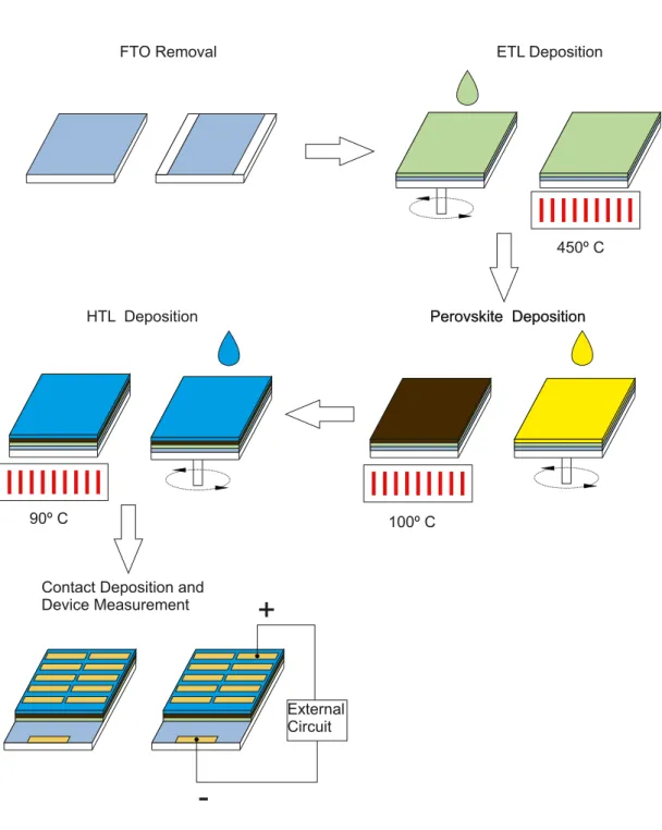
This chapter will describe in detail the experimental processes used to achieve complete solar cell devices.
The solar cells’ fabrication process can be divided into three main categories: Sub-strate Preparation, Film Deposition and Contact Deposition. All the cell layers (except for the electrodes) were deposited using spin-coating technique. Figure3.1schematically represents the most crucial steps for the solar cell fabrication procedure.
3.1 Substrate Preparation
Fluorine doped tin oxide (FTO) coated glass (100 mm x 100 mm x 2.2 mm, 13 Ω/sq,
82-84.5% transmittance), was first cut into 2.5 x 2.5 cm substrates. These substrates were then covered in Kapton tape (on the FTO side), leaving two stripes, of 3-4 mm in width, on opposite sides, to prepare for the etching. The etching procedure is described in topics below, and was adapted from Ossila website [54].
1. Prepare a 2M HCl solution;
2. Place mask onto the FTO glass substrates;
3. Apply Zinc powder onto the areas of interest;
4. Remove excess powder;
5. Place the substrate in a glass container (petri dish);
6. Coat the substrate with the 2M HCl solution;
FTO Removal ETL Deposition
Perovskite Deposition HTL Deposition
External Circuit Contact Deposition and
Device Measurement
+
-Perovskite Deposition 450º C
100º C 90º C
3 . 2 . F I L M D E P O S I T I O N
8. With an cotton bud, wipe the etched area;
9. Remove mask;
10. Clean substrate with a cotton bud soaked in IPA.
The end result of this procedure is represented in figure3.2.
Figure 3.2: Glass substrate after FTO removal - In grey: un-etched FTO film; In blue: etched areas(glass only).
Prior to the ETL deposition, the substrates were cleaned using ultrasonic baths. The first bath contained DI water and detergent and lasted for 15 minutes at 50° C. After, the substrates were rinsed in a DI water bath for 15 minutes at 50° C. The substrates were then transferred onto an Acetone bath, followed by an IPA bath, both at 50°C for 15 minutes. The glass substrates were rinsed in DI water and dried using a nitrogen gun, before being submitted to UV treatment for 15 minutes as the final cleaning step, improving at the same time the wettability of the substrate.
3.2 Film deposition
This section will report, in order of deposition, the processes related to the fabrication of each film/layer of the solar cells.
3.2.1 ETL deposition
For the ETL deposition the material of choice was TiO2and two different solutions were
to obtain similar thickness [55]. After the spin-step, the substrates were dried for 10 minutes, at 120° C and then annealed at 450° C for 30 minutes on a hot-plate, in ambient air conditions.
It was also tested the use of a mesoporous layer to see if it would improve the device performance. The solution is described as well in appendixB, and the spin-step, dry-step and annealing conditions were the same as for the compact layer using the TTIP.
3.2.2 Perovskite deposition
For the active layer, a few different solutions were tested, varying from different
concen-trations, to different solvents and reagents. For the MACl study, various concentrations
were used, but for MAI only two were tested, and for full solar cell devices only the 1M solution was used. All the details for the used solutions are in appendixB.
For this work it was employed a technique called "Solution aging", where the precursor solution is prepared in advance to the deposition, with precise timing. For this work a 24 hour aging was used, meaning the solution was prepared and left to stir at 70° C for 24 hours. Prior to the spin-step, the substrates were also heated to 70°C (Hot-casting method). Higher temperatures were tested using the MACl precursor solution (90° C and 100° C), but the solution would evaporate too quickly on the substrate before the substrate was made to spin, especially at 100° C and as such, they were eliminated from following studies.
A precursor solution volume of 150 µl when using the MACl solution, and 120 µl for the MAI solution, was spin-coated onto the substrate using a two-step spinning program. For the MACl solution the spinning program consisted of a first step of 2500 rpm for 15 s (2000 rpm/s ramp) followed by a 5000 rpm for 25 s (4000 rpm/s) step. In the case of the MAI solution it was first used a spinning step of 1000 rpm for 10 s (500 rpm/s ramp) followed by 6000 rpm for 20 s (5000 rpm/s ramp) step. During the second stage of the spinning process, different anti-solvent agents were dispersed onto the substrate.
It was also tested using an anti-solvent on the first stage of the spinning step. This will be described in further detail on chapter4.
The final step for the active layer is the annealing, which was done at 100° C for 10 minutes in the MACl case and it was tested 15 and 60 minutes using MAI solution.
3.2.3 HTL deposition
CuSCN was used as the material for the HTL. Two different solutions were tested and
3 . 3 . CO N TAC T D E P O S I T I O N
the substrate after the first 5 s of spinning, where the parameters are: 5000 rpms (4500 rpm/s ramp) for 30 s. Annealing of this layer is done at 90° C for 30 minutes in ambient air conditions.
3.3 Contact deposition
The final step in order to complete the solar cells is to deposit the gold contacts. Acetate masks illustrated in figure 3.3, designed using CorelDRAW software, were cut using a CO2 LASER (from Universal Systems) and placed onto the devices prior to gold
de-position. The deposition was achieved through electron-beam evaporation in working pressure of 10−5mbar and it was deposited 80-100 nm of gold for the back and front
con-tacts. The end result of the devices is represented in figure3.4. As the contacts were also one of the key tasks for this work, further details of the contact process will be presented and analyzed in chapter4.
a b
Figure 3.3: a) Masks used in the original version of the contacts (opening for contacts: 8x0.6 mm2); b) Masks used for the new contact version (opening for contacts: 10x1 mm2).
3.4 Characterization
In this section it is presented the characterization techniques and the respective equip-ment, used throughout this work.
3.4.1 SEM analysis
a b c
Figure 3.4: a) SC device using original contact version; b) SC device using etching/perimeter-mask version; c) SC device using final version; In white are the ar-eas that remain film-free; In grayish-blue FTO-only arar-eas; In dark-brown is represented the effective device area (area where all the layers are deposited; In gold are represented
the different deposited contacts.
3.4.2 UV-Vis Spectroscopy
The optical characterization of the films was achieved using a Shimadzu UV 3101PC. To obtain absorbance spectra, an ISR-260 Integrating Sphere was used in order to obtain Total Transmittance and Reflectance spectra within a 300-830 nm range. The thickness estimation for the TiO2 compact layer was obtained through optical simulations with
TMM, using Mathematica software, developed by Professor Manuel Mendes.
3.4.3 XRD analysis
Structural analysis of Perovskite films was achieved through X-ray Difraction (XRD) us-ing a PANalytical X’Pert Pro X-ray diffractometer in Bragg-Brentano geometry, with a
monochromatic Cu-Kα radiation source (1.5406 Å). The resulting diffractogram was
acquired using the High Score Plus software (PANalytical).
3.4.4 Electrical characterization
C
h
a
p
t
e
r
4
R e s u lt s a n d D i s c u s s i o n
This chapter will be divided into three main sections, as these were the main goals throughout the thesis. In each section it will be presented the corresponding results, as well as these being interpreted and discussed, terminating with a few conclusions about the results.
The first section will address the processes of fabrication of the front and back contacts, as this was thought to be one of the key reasons as to why the devices developed until this stage were not achieving the desired performance.
The middle section focuses on the study of MACl as a possible viable replacement of MAI, in Perovskite synthesis for future devices.
The third section will report the efforts on one of the major objectives of this master
thesis: the optimization of the devices obtained in the previous work.
The results presented in this chapter will not be chronologically in order, and as such, the results from each section can be correlated only to an extent.
4.1 Solar Cell Contacts
As it was already mentioned, the contacts were thought to be hurting the performance of the devices, particularly, the back contacts. The measuring tips, with which the I-V measures were taken, could have been penetrating the gold contacts and thus, damaging the underlying films, ultimately reaching the FTO film, causing a short-circuit and invali-dating the measurement. In order to prevent this from happening, a new type of contacts needed to be thought of, one that could deal with the fact that the measuring tips could penetrate the films.
zone of the device. A few trials were made in that sense, using different processes [56,57],
until there was success removing the FTO through the process described in full detail in
3.1. The resulting substrate is illustrated in figure3.2.
Following the successful removal of the FTO stripes, after a few test versions diverging mainly on number and position of contacts, a new mask design was created (3.3b) to replace the one used for the previous type of contacts (3.3a). This new mask incorporates a second front contact, to help reduce the distance between the measuring tips during the measurement, hoping to improve it.
4.1.1 Etching-Method Contacts
Initially it was used a fabrication process, reliant on keeping the stripes (areas where the FTO had been removed) film-free. This was first done by selectively removing, on the zones of interest, the film that was just spin-casted onto the substrate. This meant that, after the deposition of an individual layer and prior to the dry-step or annealing step, an etching of a "perimeter area"was done, using a cotton bud soaked in different materials,
depending on the film being removed at the time. For the TiO2 and CuSCN layers, the
respective solution solvents were used for the etching of the desired area, while for the Perovskite layer, acetone was used for the etching. The resulting substrate is shown in figure 4.1, where the blue color refers to the film-free areas, grey color referring to an area with only FTO film (front contact) and the dark-brown color referring to the effective
device area (all films present). This method shall be referred as the "Etching contact method"in this document.
Figure 4.1: Substrate resulting from the etching method, prior to gold contact deposition, with dimensions as the ones in figure 3.2. Blue color refers to film-free areas of the substrate; Grey color refers to the FTO front contacts; Dark-brown color refers to effective
device area.
4 . 1 . S O L A R C E L L CO N TAC T S
short-circuiting. Another problem that surfaced while doing this type of contact proce-dure was the clear degradation of the SC films (particularly the Perovskite film) on the film edges due to the etching, which can be observed in figure4.2. In order to test the types of contacts, a few batches were dedicated only to testing the different processes of
fabricating the contacts.
a b
Figure 4.2: Effects of the Etching contact method on film quality, presenting degradation
on film edges.
The I-V and P-V measurements for the first batch of SC devices dedicated solely to the contact testing is presented in figure 4.3, with the details of each measurement be-ing presented in table4.1. There seems to occur some abnormalities, such as a sudden drop or small rise and stabilization, in the current values towards the end of the mea-surements. It is believed (although it was not tested during this work) to be due to the electronic measurement unit, as upon measuring low currents, it automatically enters in a limiting range of current, giving out, from that point forward, the same value of current, independently on the real value. This is verified in more devices, especially in those of lower performance, as these naturally present low currents, therefore entering the limiting range of the measurement unit sooner.
The difference of the devices is very clear, pointing towards the original contact
proce-dure being the correct one. The measurements for the device with original contacts falls within the expected values according to previous work [34], but the difference with using
the etching version was not expected to be so pronounced. Only a slight variation in I-V measurements was expected before these devices were fabricated, and coupled with the fact that from the entire batch only one sample of each contact type was possible to measure (all other devices were not working), it was not possible to be concluded, using solely this batch, which contact type was best suited for the SC devices and as such, a new batch was made in order to repeat this test. The results are shown in figure4.4with the corresponding values of interest in table4.2.
0.0 0.1 0.2 0.3 0.4 0.5 0.6 0.7 0.0 0.5 1.0 1.5 2.0 2.5 3.0 3.5 4.0 4.5 5.0 5.5 C u rr e n t D e n s it y ( m A /c m 2 ) Voltage (V)
A - Original Contacts K - Etching-Method Contacts
a
0.0 0.1 0.2 0.3 0.4 0.5 0.6 0.7 0.000 0.005 0.010 0.015 0.020 0.025 0.030 0.035 P o w e r (m W ) Voltage (V)
A - Original Contacts K - Etching-Method Contacts
b
Figure 4.3: I-V a) and P-V b) measurements for solar devices differentiating on the contact
type (Etching vs Original). Devices fabricated using a compact TiO2using TTIP Solution;
Perovskite layer using 1 M Solution (MAI:PbI21:1), with 100 µl chlorobenzene droping,
annealed for 60 mins at 100°; CuSCN layer annealed at 90° for 30 mins.
Table 4.1: Performance values for the data presented in figure4.3
SC Devices Voc(V) Jsc(mA/cm2) FF Rsh(kΩ) Rs(kΩ) PCE(%)
Original contacts 0.631 5.48 0.175 1.86 3.204 0.604 Etching-Method contacts 0.073 1.54 0.187 0.511 0.910 0.021
Table 4.2: Performance values for the data presented in figure4.4
SC Devices Voc(V) Jsc(mA/cm2) FF Rsh(kΩ) Rs(kΩ) PCE(%)
4 . 1 . S O L A R C E L L CO N TAC T S
0.0 0.1 0.2 0.3 0.4 0.5 0.6 0.7 0 1 2 3 4 5 6 C u rr e n t D e n s it y ( m A / c m 2 ) Voltage (V) A - Original Contacts T - Etching-Method Contacts
a
0.0 0.1 0.2 0.3 0.4 0.5 0.6 0.7 0.000 0.005 0.010 0.015 0.020 0.025 0.030 0.035 P o w e r (m W ) Voltage (V)
A - Original Contacts T - Etching-Method Contacts
b
Figure 4.4: I-V a) and P-V b) measures for SC devices differentiating on contact type
(Etching vs Original - second attempt). Devices fabricated using a compact TiO2using
TTIP Solution; Perovskite layer using 1 M Solution (MAI:PbI21:1), with 100 µl
is the fact that from the SEM images shown in figure4.5, the film quality appears to be better on the device made using the original contact method, where it is possible to see grain-like structures on 4.5a) versus no grains on the device with the etching-method
4.5b). In figure4.6it is possible to see again the difference between the device fabricated
using the original procedure(on the right) and the one made with the etching-method(on the left).
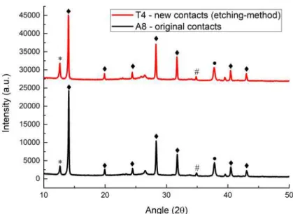
The devices were also characterized using XRD (figure 4.7) where it is possible to observe the peaks corresponding to the tetragonal phase of MAPbI3, marked with full
rhombus, the PbI2peak, marked with an asterisk, and also peaks regarding the CuSCN
and FTO layer (marked with cardinal and full circle, respectively)1[21, 24,34]. These diffractograms demonstrate a higher PbI2peak for the device fabricated using the
etching-method, indicating a higher degree of organic degradation on the perovskite film, trans-lating in a formation of a PbI2 film. This could in fact be related to the etching step
necessary for this method because, as demonstrated previously with figure4.2, the film quality tends to be inferior on the film edges due to the etching procedure. The fact that the main perovskite peaks are more intense and narrow for the device fabricated using original method contacts (values in tables4.3and4.4) helps corroborate the assumption that, using the etching-method results in films of lower quality.
Another problem with using the etching-method is the actual etching-step itself. Etch-ing the films on the designated area meant that the substrates after spinnEtch-ing, were not immediately submitted to their heating treatment (that being a dry-step or annealing step). This is especially concerning with the Perovskite films, being that it is desired a fast crystallization of the perovskite film [19,34]. Although in this work, the FDC (Fast Crystallization-Deposition) method developed by M.Xiao et al.was employed, the fact
that the substrates were not placed on the hot-plate right after the spinning step was done, could be delaying the crystallization of the films.
These results demonstrate that the contact procedure does in fact play a significant role in the quality of the device while also pointing to the fact that, although tackling the issue of damaging the films with the measuring tips during I-V measures, the new type of contacts (using the etching method) was in fact hurting the devices.
Table 4.3: Perovskite Peak Parameters of the diffractograms in 4.7 - Original Method
device.
2θ(◦) Intensity (a.u.) FWHM (◦)
14.07 22117.6 0.127
28.3 9065.1 0.149
4 . 1 . S O L A R C E L L CO N TAC T S
a b
Figure 4.5: Surface morphology influence with contact type. a) Original-Method; b) Etching-Method
Figure 4.6: Difference between devices using the etching-method (on the left) and the
original contact process (on the right).
Table 4.4: Perovskite Peak Parameters of the diffractograms in 4.7 - Etching Method
device.
2θ(◦) Intensity (a.u.) FWHM (◦)
14.07 17164.6 0.130
Figure 4.7: XRD diffractograms - Contact Study: Etching-Method vs Original Method.
Peaks corresponding to the tetragonal phase of MAPbI3, marked with full rhombus, the
PbI2peak, marked with an asterisk and also peaks regarding the CuSCN and FTO layer
(marked with cardinal and full circle, respectively).
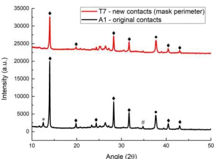
4.1.2 Perimeter-Mask-Method Contacts
The results from4.1.1made it clear that the etching-method was not the correct procedure for the contacts on the SC devices and as such, a different approach was needed, one that
still tackled the issue of the possible film damage during the I-V measurements, while avoiding the film degradation that resulted from the etching-method.
As discussed previously, the actual etching step was the main problem with that specific contact procedure and as such, the new approach for the contacts envisioned removing all together this step.
The solution found was instead of removing (etching) the films after each deposition, the areas of interest (lateral stripes of glass only and FTO areas for the front contact) would remain film-free throughout the entire film deposition process. This was done by taping Kapton masks on the designated areas, removing them only before the gold contact deposition step. The resulting substrate is represented in figure 4.8, where in yellow color is represented the Kapton mask and in dark-brown the SC films. This particular contact method shall be referred as "Perimeter-Mask-Method". This method allows for a more controlled film-free area and it does not introduce a intermediate step between the spinning and the annealing treatments of each film (the substrate is moved directly to the hot-plate after the spin step).
![Figure 2.1: General working principle of a solar cell [14].](https://thumb-eu.123doks.com/thumbv2/123dok_br/16538623.736629/28.892.187.705.617.1026/figure-general-working-principle-solar-cell.webp)
![Figure 2.3: Perovskite Crystal Structure; a)Perovskite unit cell [17]; b) Crystal Structure of cubic metal halide Perovskite (ABX 3 ) [18].](https://thumb-eu.123doks.com/thumbv2/123dok_br/16538623.736629/30.892.211.686.476.974/figure-perovskite-crystal-structure-perovskite-crystal-structure-perovskite.webp)
![Figure 2.4: Energy level alignment for some of the materials used in this work; Schematic band-bending of energy levels [37–40]](https://thumb-eu.123doks.com/thumbv2/123dok_br/16538623.736629/33.892.147.762.702.1072/figure-energy-alignment-materials-schematic-bending-energy-levels.webp)
![Figure 2.6: Schematic thin film deposition via E-beam technique [48].](https://thumb-eu.123doks.com/thumbv2/123dok_br/16538623.736629/36.892.261.629.232.510/figure-schematic-thin-film-deposition-via-beam-technique.webp)