982 Brazilian Journal of Physics, vol. 36, no. 3B, September, 2006
Electrical and Morphological Properties of Low Resistivity Mo thin Films
Prepared by Magnetron Sputtering
G. Gordillo, F. Mesa, and C. Calder´on
Departamento de F´ısica, Universidad Nacional de Colombia, Bogot´a, Colombia
Received on 8 December, 2005
Mo thin films have been deposited using a DC magnetron sputtering system with an S-gun configuration electrode and characterized electrically and morphologically. The influence of the sputtering gas pressure and glow discharge (GD) power, on the electrical resistivity of Mo thin films and on the contact resistivity of Mo to Cu(In,Ga)Se2(CIGS) films was determined through an exhaustive parameter study. This study also allowed
us to find the conditions to deposit Mo films with suitable properties for its use as back contact of solar cells based on CIGS. Resistivities smaller than 1x10⁻⁴ Ω.cm and contact resistivities smaller than 0.3Ωcm2were
found. Mo films with these characteristics are suitable for back contacts in solar cells based on CIGS. It was also found that the Mo thin films, deposited by DC magnetron sputtering on CIGS thin films, act effectively as ohmic contacts. The main contribution of this work was to obtain Mo thin films with adequate properties to be used as back contact for CIGS based solar cells using a DC sputtering system with S-gun configuration electrode, which allows growing the film with better surface quality and at a higher deposition rate than those deposited using the conventional planar RF sputtering system.
Keywords: Mo; Thin films; Solar cells; CIGS; Low resistivity
I. INTRODUCTION
Several metals, Pt, Au, Ag, Cu and Mo, have been investi-gated for using as electrical contact of CuInSe2(CIS) and its
gallium alloy (CIGS)-based solar cells [1-3]. Mo emerged as the dominant choice for back contact layer of CIS and CIGS solar cells because of its relative stability at the processing temperature, resistance to alloying with Cu and In, and its low contact resistance to CIGS. Efficiencies greater than 19% have been reported for this type of devices fabricated using Mo films, deposited by conventional rf magnetron sputtering, as ohmic back contact [4,5].
Some authors [6,7] have reported that a Schottky barrier is formed when Mo films are inadequately deposited on CIGS films. When a Schottky barrier is formed at the CIGS/Mo contact, substantial resistive losses occur, affecting negatively the device efficiency.
In this work we investigate how deposition parameters, such as pressure of the sputtering gas and power supplied to the sputtering system, influence the conductivity of the molyb-denum films and the contact resistivity of the Mo/CIGS sys-tem. Through an exhaustive parameter study, conditions were found to get Mo films, which form ohmic contact on CIGS films.
II. EXPERIMENTAL
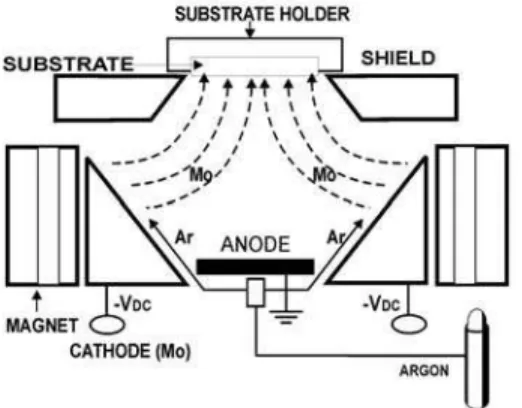
Molybdenum films were prepared using a DC magnetron sputtering system with an S-gun configuration electrode. The main difference of this system with the conventional planar rf sputtering systems, is that the S-gun configuration employs a central anode surrounded by an Mo cathode 99.9% pure, which presents a conic shaped concavity. Fig. 1 shows a di-agram of the sputtering system used to prepare the molybde-num films. In this system the films are deposited outside the
plasma region which allows growing them with better surface quality than using the sputtering system with planar electrode configuration. On the other hand, the deposition rate of the films grown using the system with S-gun configuration is sig-nificantly greater than those deposited using the conventional system with planar electrode configuration.
The deposition chamber was evacuated by a turbo-molecular pump to a base pressure of 10−5mbar and the Ar-partial pressure was electronically controlled, using an auto-matic control system consisting of a Balzers RV6 040 regu-lating unit and an RME 010 reguregu-lating valve. Table I lists the deposition parameters of the molybdenum films and their ranges of variation.
The CIGS films were deposited through a chemical reaction of the precursor species, which were evaporated sequentially in a three-stage process [8]. In the first stage the elements In, Ga and Se are evaporated simultaneously on a substrate heated at 300oC. During this stage a thin film of the
com-pound (In,Ga)xSey is formed. In the second stage, Cu and
Se are simultaneously deposited on the layer formed in the previous stage, keeping the substrate temperature at 600oC. During the second stage the compound Cu(In,Ga)Se2is
pre-dominantly formed. However, secondary phases of Cu and In selenides are also formed. Finally, in a third stage In, Ga and Se are simultaneously evaporated at a substrate temper-ature of 600oC (at lower rates than in the first stage), in
or-der to optimize the chemical composition of the CIGS films. The deposition process of the CIGS films is controlled with a thickness monitor (Maxtec TM-400), which uses a quartz crystal as sensor.
The film conductivity was measured using a standard four-point probe method to determine the resistance, and a Dektak profilometer was used to determine the thickness. The contact resistanceRCof Mo on p-CIGS thin films was determined
characteris-G. Gordillo, F. Mesa, and C. Calder´on 983
FIG. 1: Schematic diagram of the sputtering system with S-gun con-figuration electrode.
TABLE I: List of the deposition parameters and corresponding vari-ation ranges, used to deposit the Mo thin films.
Parameters Variation range
Substrate temperature Room temperature Glow discharge power (W) 50 - 200
Sputtering current (mA) 600 - 700
Ar- partial pressure (mbar) 1.1x10⁻²- 1.6x10⁻²
Bias voltaje (V) 30 - 80 Deposition time (min) 6 - 26
tic and contact resistanceRC. For ohmic contacts, the contact
resistivityRC, defined as [9]
ρC= dV dJ V =0
=RCAC
Ωcm2
can be obtained from the slope of the J-V curve at zero bias, whereACis the contact area. The study of the morphological
properties was carried out with a Park Scientific AFM micro-scope.
III. RESULTS AND DISCUSSION
A. Electrical and morphological properties
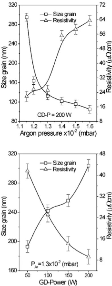
The effect of the working gas pressure and the glow dis-charge power on the electrical resistivity was studied in an attempt to find the deposition conditions to get low resistive Mo thin films. For that, Mo thin films were deposited varying the pressure from 1x10⁻²to 1.6x10⁻²mbar and the glow dis-charge (GD) power from 50 to 200 W. The results indicated that the resistivity of the Mo films decreases by increasing the GD-power or by decreasing the Ar-pressure (see Fig. 3). On the other hand, measurements of the Mo films grain size, car-ried out with an AFM microscope, showed that this parameter increases by both, decreasing the Ar-pressure and increasing
the GD-power. This result indicates that the reduction of the resistivity could be attributed, in part, to an increment of the grain size. In fig. 2 are depicted AFM images showing the influence of the working gas pressure and GD- power on the morphology of the Mo films.
The AFM studies showed clearly that the Ar-pressure and the GD-power affect the morphology of Mo films deposited by DC magnetron sputtering (with configuration S-Gun). In Fig. 3 are depicted curves that show the effect of the Ar-pressure and the GD-power on both, the electrical resistivity of Mo films and the grain size.
It is observed, correlating the curves of resistivity with those of grain size, that the decrease in resistivity of the Mo films is accompanied by an increase of the grain size. This behavior could be explained by assuming that increasing the grain size increases the carrier mobility of the Mo films. It seems that the increase of the grain size of the Mo films in-duces a reduction of the grain boundary potential barrier’s height, as well as the number of grain boundaries the carrier has to cross during electrical transport, which, in turn, leads to a decrease of the resistivity.
Figure 4 shows results indicating that increasing the film thickness can also reduce the resistivity of the Mo-films. This behavior could be also attributed to an increase of the carrier mobility induced by increasing the grain size.
The lowest resistivity value we found for the Mo films was 9x10⁻⁶ Ωcm. This was obtained with Mo films prepared at Ar-pressure of 1.15x10⁻²mbar and a target power of 200 W. Values of 1.6x10⁻⁵Ωcm have been reported [6] for Mo-films deposited on soda-lime glass substrates by planar RF mag-netron sputtering and of 1.1x10⁻⁵ Ωcm for Mo-films de-posited by planar DC magnetron sputtering.
B. Contact resistivity of Mo to Cu(In,Ga)Se2films
The Mo films will be used as back contact layers for the Cu(In,Ga)Se2 based solar cells, and the best parameter
to characterize the quality of an ohmic contact is its con-tact resistivityρC [11]. So, the influence of the chemical
composition (Ga-content) on the contact resistivity of Mo to CuInxGa1−xSe2thin films was also studied.
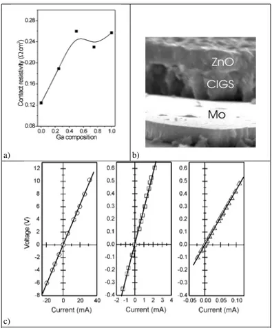
Figure 5 depicts a curve of the contact resistivity of Mo on CuInxGa1−xSe2 thin films as a function of the chemical composition x. In Fig. 5 are shown curves of I vs. V, carried out to judge if the contact of Mo to Cu(In,Ga)Se2thin films
is ohmic. The Mo films were deposited on the Cu(In,Ga)Se2
films using the deposition parameters leading to the lowest resistivity value (1.15x10⁻²mbar and 200 W).
The results of Fig. 5 indicate that the contact resistivity of Mo to CuInxGa1−xSe2 thin films increases by increasing the Ga content. However, the values ofρC obtained in this
work were lower than 0.3Ωcm2, which is quite acceptable for
ohmic contacts in solar cells. The linear behavior of the I-V curves confirms its ohmic character.
984 Brazilian Journal of Physics, vol. 36, no. 3B, September, 2006
FIG. 2: Typical AFM images of Mo thin films, showing the effect of the Ar-partial pressure and of the GD-power on the morphology. a) P=100 W, Ar-p=1.6x10⁻²mbar b) P=100 W, Ar-p=1.15x10⁻²mbar
c) Ar-p=1x10⁻²mbar, P=50 W d) Ar-p=1x10⁻²mbar, P=200 W.
with efficiencies close to 9% [12].
IV. CONCLUSIONS
Molybdenum thin films with adequate properties to be used as electrical back contact of solar cells based on CIGS were grown using a DC magnetron sputtering system with an S-gun configuration electrode. The results indicated that it is possi-ble to get low resistivity Mo films by decreasing the Ar par-tial pressure and increasing the power of the glow discharge. This behavior is mainly attributed to an increase of the film grain size. The lowest value obtained for the resistivity was 9x10⁻⁶ Ωcm, which is lower than those reported in the lit-erature for Mo films deposited by other methods. It was also found that the contact resistivityρCof the Mo/CIGS system is
increased by increasing the Ga content; however, the values of
ρCwe obtained for the CIGS films were lower than 0.3Ωcm2;
these values ofρCare quite acceptable for ohmic contacts of
FIG. 3: Variation of the resistivity and grain size of Mo films as a function of a) Ar-pressure and b) GD-power.
G. Gordillo, F. Mesa, and C. Calder´on 985
a) b)
c)
FIG. 5.a) Variation of the contact resistivity of Mo to CuInxGa1−xSe2thin
films as a function of the chemical composition (x value), b) SEM micro-graph of the cross section of a solar cell with structure Mo/CIGS/ZnO and c) curves of I vs. V of the system Mo/CuInxGa1−xSe2, for x=0, 0.5 and 1
respectively.
solar cells operating at small solar concentration ratios. I vs. V measurements carried out with the Mo/CIGS/Mo system indicated a linear behavior, confirming the ohmic character of Mo on CIGS films.
Acknowledgements
The Universidad Nacional de Colombia and Colciencias supported this work.
[1] J.H. Scofield, A. Duda, D. Albin, B. L. Ballard and P. K. Pre-decki, Thin Solid Films260, 26 (1995).
[2] R. J. Matson, O. Jamjoum, A. D. Buonaquisti, P. E. Russell et al., Solar Cells11, 301 (1984).
[3] E. Moons, T. Engelhard and D. Cahen, J. Electron. Mater.22 (3), 275 (1993).
[4] L.L. Kazmerski, Journal of Electron Spectroscopy and Related Phenomena150, 105 (2006).
[5] K. Ramanathan, M. Contreras, I. Perkins, S Asher et. al., Progress in Photovoltaics: Res. Appl.11, 225 (2003). [6] W. Jaegaermann, T. Lher, C. Pettenkofer, Cryst. Res. Technol.
31, 273 (1996).
[7] T. Wada, N. Kohara, S. Nishiwaki and T. Negami, Thin Solid Films387, 118 (2001).
[8] M.A. Contreras, B. Egaas, K. Ramanathan, J. Hiltner, A. Zwart-lander, F. S. Hasoon, and R. Nuofi, Progress in Photovoltaics: Research and applications,7, 311 (1999).
[9] A. L. Fahrenbruch, R. H. Bube,Fundamentals of Solar Cells,
Academic Press, New York, (1992).
[10] T.C. Anthony, A.L. Fahrenbruch, and R. Bube, J. Electronic Mater.11, 89 (1982).
[11] A. Musa, J. P. Ponpon, J. J. Grob, M. Hage-Ali et al., J. Appl. Phys.54(6), 3260 (1983).