252 B. G. Enders et al.
Effect of non-abrupt doping and interfacial profiles on the carrier sheet density in one-side
modulation-doped GaN/AlGaN quantum wells
B. G. Enders, F. M. S. Lima, A. L. A. Fonseca, and O. A. C. Nunes Instituto de F´ısica, Universidade de Bras´ılia, Cx. Postal 04455,
70919-970, Bras´ılia, DF, Brazil
E. F. da Silva Jr. Departamento de F´ısica,
Universidade Federal de Pernambuco, Cidade Universit´aria 50670-901, Recife, PE, Brazil
(Received on 1 September, 2008)
The results of an accurate theoretical study on the effects of non-abrupt doping and interfacial profiles on the electron sheet density in one-side modulation-doped wurtzite GaN/AlGaN single quantum wells at low temperatures are presented. We solve coupled Schr¨odinger and Poisson equations self-consistently via the finite difference method. By employing a proper discretization on a nonuniform grid and taking into account the strong piezoelectric and spontaneous polarization fields exhibited by the wurtzite III-nitride heterostructures, a substantial increase in the 2DEG density is predicted with the increase of the donor diffusion length and the reduction of the spacer thickness.
Keywords: non-abrupt doping; interfacial profiles; carrier sheet density; quantum wells
1. INTRODUCTION
The effects of non-abrupt doping and interfacial profiles on the performance of a variety of electronic devices have been already identified [1, 2]. It was found, for example, that high-electron mobility transistors (HEMTs) have their thresh-old voltage and the rate of gate-voltage switching strongly dependent on the composition and the doping profile along the growth direction [3], which also affects the performance of one-side modulation-doped quantum well (QW) infrared photodetectors [4]. Theoretically, better device performances should be observed with the use of heterostructures with abrupt doping profiles, a fact that made the reduction of im-purity interdiffusion an important research topic in semicon-ductor physics. However, there are experimental evidences indicating that the actual doping profiles are not abrupt [5, 6] and this is due to limitations in the control of impurity implan-tation during the growth process, as well as to dopant diffu-sion/segregation during the deposition and posterior anneal-ing [7, 8]. Additionally, there is also experimental evidence supporting the existence of graded interfaces in GaN/AlGaN quantum wells [9, 10].
In this work, we present the results of an accurate theo-retical study on the effects of non-abrupt doping and inter-facial profiles on the electron sheet density in a graded one-side modulation-doped GaN/AlGaN QW at low temperature. The electronic subband structure is determined by solving the coupled Schr¨odinger and Poisson differential equations self-consistently via finite difference method (FDM), employing a proper discretization on a nonuniform grid [11], and taking into account the strong piezoelectric and spontaneous polar-ization fields exhibited by the wurtzite III-nitride heterostruc-tures [12]. Emphasis is given on the dependence of the carri-ers sheet density on both the spacer thickness and the donors diffusion length.
2. GOVERNING EQUATIONS
The electron eigenstates are calculated self-consistently by solving the one-electron Schr¨odinger equation within the ef-fective mass and Hartree approximations [13] along with the Poisson equation for the quantum well under consideration at a given temperature and for a given graded distribution of donor impurities. A linear variation of the alloy molar frac-tionxinto the heterointerfaces is considered (see Fig. 1). As there are differences in both the carrier effective mass and the dielectric constant along the growth direction (chosen here as thez-axis), the BenDaniel-Duke Hamiltonian [14] for the Schr¨odinger equation must be employed, yielding
−~ 2
2 d dz
1 m∗(z)
dψj(z)
dz
+V(z)ψj(z) =Ejψj(z), (1)
where~is the reduced Plank constant,m∗(z)is the position-dependent effective mass,ψj(z)is the envelope wavefunction
for the j-th subband, Ej is the corresponding energy
eigen-value, andV(z) =V0(z) +VH(z)is the potential energy,V0(z)
being the potential energy before the charge transfer process andVH(z)being the Hartree potential.
The Hartree potential is the solution of the Poisson equa-tion. As the dielectric constant varies along thez-axis, one has to make use of the generalized Poisson equation [15], which reads
d dzε(z)
d
dzVH(z) = e2 ε0
ND+(z)−n(z)
, (2)
where ε(z) is the position-dependent dielectric constant, e is the elementary charge, and ε0 is the vacuum
permittiv-ity constant. The charge concentrations on the right-hand side of Eq.(2) are ND+(z), for ionized donors, and n(z) =
∑Jj=1N (j)
s |ψj(z)|2, for electrons, jbeing the subband index,
Ns(j)being the carrier sheet density at the j-th subband, andJ
identifies the highest occupied subband.
Brazilian Journal of Physics, vol. 39, no. 1A, April, 2009 253
FIG. 1: The linear interfacial profile adopted for the alloy molar frac-tion variafrac-tion in a single graded GaN/AlGaN QW with asymmetric interfaces of thicknessesw1andw2.
form of polarization fields, which are included in the bare potential as follows:
V0(z) =
eFbz+∆Ec, forz<0
eFwz, for 0<z<Lw
e(Fbz+FwLw) +∆Ec forz>Lw
(3)
whereLw(Lb) is the well (barrier) width,Fw(Fb) is the
mag-nitude of the electric field in the well (barrier), and∆Ecis the
GaN-AlGaN conduction-band offset, assumed to be given by ∆Ec=0.75[Eg(x)−Eg(0)][16, 17], where [18]
Eg(x) =6.13x+3.42(1−x)−1.0x(1−x) (4)
is the AlxGa1−xN band gap in eV.
By considering that the overall potential drop across the structure has to be null, i.e.FwLw+FbLb=0, then the
polar-ization fields can be written in terms of the total polarpolar-ization in the well,Pw, and in the barrier,Pb, as [19]:
Fw,b=
(Pb,w−Pw,b)Lb,w
εw,bLb,w+εb,wLw,b
, (5)
in whichεw(εb) is the dielectric constant of the well (barrier).
The total polarizations can be calculated directly by the sum of the piezoelectric (Ppz) and spontaneous (Psp) polarizations of the corresponding layers:
Pw,b=P sp w,b+P
pz
w,b. (6)
For AlxGa1−xN/GaN QWs grown on GaN buffer we have
Pwpz=0 andPwsp=−0.034 C/m2, and the remaining
polariza-tion expressions for the strained alloy can be written as (in C/m2) [18]
Pbsp(x) =−0.090x−0.034(1−x) +0.021x(1−x), (7)
Pbpz(x) =2a(x)−a0 a0
e31(x)−e33(x)C13(x) C33(x)
, (8)
wherea(x)is the basal lattice constant of the wurtzite III-nitride alloy, a0 is the lattice constant of the GaN buffer, e31,e33 are the piezoelectric constants and C13,C33 are the
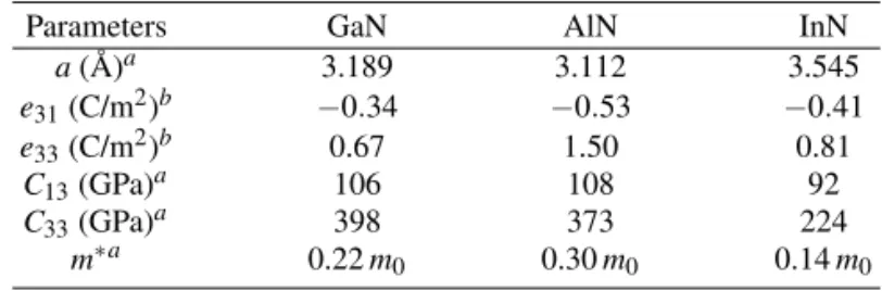
elastic constants [20]. These parameters are predicted to fol-low the composition-weighted average between the relevant binary compound values, i.e. Vegard’s rule. These values are presented in Tab. I.
In the depletion approximation, it is considered that all im-purities are ionized within a layer of widthLD [23]. In this
TABLE I: Wurtzite nitride binaries parameters considered in the composition-weighted average used in the determination of the ternary nitride alloys parameters.
Parameters GaN AlN InN
a( ˚A)a 3.189 3.112 3.545
e31(C/m2)b −0.34 −0.53 −0.41
e33(C/m2)b 0.67 1.50 0.81
C13(GPa)a 106 108 92
C33(GPa)a 398 373 224
m∗a 0.22m0 0.30m0 0.14m0
aRef. 21. bRef. 22.
work we have surpassed this approximation by considering a more realistic position-dependent concentration of ionized impurities as given by [24]
ND+(z) = ND(z)
1+2 exphEF+ED−V(z)
kBT
i, (9) in whichEDin the donor ionization energy,EFis the Fermi
level,T is the temperature, andND(z)is the total
concentra-tion of impurities, described here by means of a normalized error function, erf(x), via the following expression:
ND(z) =
ND0 2
1−erf
z+Ls
2Dl
, (10)
where Dl is the donor diffusion length, ND0 is the nominal
doping concentration, andLsis the spacer thickness.
Finally, the 2DEG areal density in each subband is obtained by means of
Ns(j)=
m∗kBT
π~2 ln
1+exp
E
F−Ej
kBT
. (11)
Having established the governing equations, we can now apply the FDM for solving Eqs. (1) and (2) for a GaN/AlGaN QW in a self-consistent manner. In doing this, it was shown that stable and accurate numerical results are obtained only if the so-called proper discretization is adopted [14]. We veri-fied that such discretization may be generalized for nonuni-form meshes in order to achieve an even higher level of pre-cision and stability [11]. For the Schr¨odinger equation, the following difference equation was adopted:
−~ 2
2 h
aiψ(i−j)1−(ai+bi)ψ(ij)+biψ(i+1j)
i
+Viψ(ij)=Ejψ(ij),
(12) where the index i identifies the grid points along thez-axis direction. The auxiliary parametersaiandbiare given by
ai≡
m∗i−1/2∆zi∆zi+1/2
−1
(13) bi≡
m∗i+1/2∆zi+1∆zi+1/2
−1
, (14)
with
m∗i±1/2=m
∗
i +m∗i±1
2 (15)
∆zi+1/2=∆zi+∆zi+1
254 B. G. Enders et al.
FIG. 2: Dependence of electron sheet density on spacer thickness in a 60 ˚A wide graded GaN/Al0.8Ga0.2N QW with a normal interface
width ofw1=3 ML and an inverted interface width ofw2=4 ML.
The nominal donor concentration isND0=6×1018cm−3.
where∆zi represents the i-th mesh step size. By using the
same discretization procedure for the generalized Poisson equation, one has
εi−1/2
∆zi
VHi−1−
ε
i−1/2
∆zi
+εi+1/2
∆zi+1
VHi+
εi+1/2
∆zi+1 VHi+1
=e 2
ε0
∆zi+1/2ND+ i−ni
, (17) where
εi±1/2=
εi+εi±1
2 . (18)
The charge transfer iterations are simulated by successive changes in the quasi-Fermi levels in both the well and the barrier layers, until the difference between them is reduced to less than a small chosen tolerance, when the thermodynamic equilibrium is reached.
3. RESULTS AND DISCUSSION
In Fig. 2, the dependence of the carriers sheet density (=∑Jj=1N
(j)
s ) onLsis shown for a 60 ˚A-wide wurtzite graded
GaN/Al0.2Ga0.8N QW with a normal interface width ofw1=
3 ML and an inverted interface width of w2 =4 ML (see
Fig. 1), one monolayer (ML) for GaN being 2.59 ˚A long. The dashed line corresponds to the abrupt doping profile in the depletion approximation while solid lines are related to the non-abrupt doping profiles with donors diffusion length ofDl=20 ˚A(thin line) andDl=40 ˚A(thick line). A nominal
donor concentration ofND0=6×1018cm−3was considered. As seen in Fig. 2, for all values of Dl the 2DEG density
decreases rapidly forLs below, say, 60 ˚A. Note also that the
2DEG density increases significantly with the increase ofDl
from 0 (abrupt) to 40 ˚A. The increase ofLstends to bring the
curves closer due to the reduction of the effect of the non-abruptness of the doping profile on the charge transfer pro-cess.
Hence, a significant increase inNs(up to 64% forLs≈30 ˚A)
is predicted when non-abrupt doping profiles are taken into
account. Though this demands more elaborate computational programming, the more realistic results obtained with our non-abrupt model have sufficient accuracy for a consistent comparison with experimental data forNs, which can be
per-formed in, e.g., Shubnikov-de Haas and Hall experiments. In-cidentally, the increase inNsas a consequence of the use of a
non-abrupt doping profile predicted here shows that the theo-retical underestimation of this quantity obtained with models based upon abrupt profiles should not be attributed solely to the presence ofDXcenters, as suggested by Ref. [25].
It must be emphasized that our nonuniform mesh choice is also important for obtaining a better simulation of the charge transfer process, since it has allowed us to allocate more points into the depletion region.
We also noted that the wave function penetration into the doped AlGaN barrier increases when a non-abrupt doping profile is adopted. This can be attributed to an increase in the number of ionized donors in the proximities of the 2DEG af-ter the charge transfer process. Since this clearly increases the electron-ionized remote donors scattering rate, the electron mobility is reduced. Then our model makes way for more re-alistic simulations of electron transport in modulation-doped heterostructures.
For simplicity, we have not included residual acceptors in our self-consistent model. This is a point to be considered in future works, since it has been shown that the presence of background impurities can affect both the 2DEG density and the electron mobility in GaAs/AlGaAs one-side modulation-doped QWs [26]. To what extent this occurs in GaN/AlGaN one-side modulation-doped QWs is not well established in literature.
4. CONCLUSIONS
In this work, we present accurate self-consistent results for the dependence of the sheet density on the doping and inter-facial profiles for electrons in a modulation-doped wurtzite GaN/AlGaN QW under the effects of the intrinsic polariza-tion fields. A substantial increase in the 2DEG density is pre-dicted for smaller spacer width and higher donor diffusion length. Other non-abrupt profiles for both interface and the doping are to be investigated. Since the effect on the 2DEG density is measurable, we expect availability of experimental results to fit our calculations.
Since the electrical characteristics of modulation-doped QWs greatly depend on the doping distribution [27], it is, in fact, important to include the impurity diffusion/segregation in the design of modulation-doped QWs-based electronic de-vices via the adoption of non-abrupt doping profiles.
5. ACKNOWLEDGMENTS
Brazilian Journal of Physics, vol. 39, no. 1A, April, 2009 255
[1] Y. M. Park, Y. J. Park, K. M. Kim, J. C. Shin, E. K. Kim, M. H. Son, S. W. Hwang, and K. H. Yoo, Jpn. J. Appl. Phys.41, 4375 (2002).
[2] E. C. Ferreira, J. A. P. da Costa, J. A. K. Freire, G. A. Farias, and V. N. Freire, Appl. Surf. Sci.190, 191 (2002).
[3] V. V. Mitin, V. A. Kochelap, and M. A. Stroscio, Quantum Heterostructures: Microelectronics and Optoelectronics (Cam-bridge University Press, New York, 1999).
[4] E. Luna, A. Guzman, J. L. Sanchez-Rojas, J. M. G. Tijero, R. Hey, J. Hernando, and E. Munoz, J. Vac. Sci. Technol. B
21, 883 (2003).
[5] G. E. Kohnke, M. W. Koch, C. E. C. Wood, and G. W. Wicks, Appl. Phys. Lett.66, 2786 (1995).
[6] Y. Huang, C. C. Williams, and J. Slinkman, Appl. Phys. Lett.
66, 344 (1995).
[7] P. A. Sundqvist, V. Narayan, S. Stafstrom, and M. Willander, Phys. Rev. B67, 165330 (2003).
[8] J. S. Song, S. H. Seo, M. H. Oh, J. H. Chang, M. W. Cho, and T. Yao, J. Cryst. Growth261, 159 (2004).
[9] C. Kisielowski, Z. Liliental-Weber, and S. Nakamura, Jpn. J. Appl. Phys.36, 6932 (1997).
[10] T. Shirasawa, N. Mochida, A. Inoue, T. Honda, T. Sakaguchi, F. Koyama, and K. Iga, J. Cryst. Growth190, 124 (1998). [11] F. M. S. Lima, B. G. Enders, A. L. A. Fonseca, O. A. C. Nunes,
V. N. Freire, J. A. K. Freire, G. A. Farias, and E. F. da Silva, Phys. Status Solidi C1, S215 (2004).
[12] F. Bernardini, V. Fiorentini, and D. Vanderbilt, Phys. Rev. B
56, 10024 (1997).
[13] G. Bastard,Wave Mechanics Applied to Semiconductor
Het-erostructures(Halsted, New York, 1988).
[14] T. L. Li and K. J. Kuhn, J. Comput. Phys.110, 292 (1994). [15] L. Bouzaiene, L. Sfaxi, H. Sghaeir, and H. Maaref, J. Appl.
Phys.85, 8223 (1999).
[16] G. Martin, A. Botchkarev, A. Rockett, and H. Morkoc¸, Appl. Phys. Lett.68, 2541 (1996).
[17] N. Maeda, T. Nishida, N. Kobayashi, and M. Tomizawa, Appl. Phys. Lett.73, 1856 (1998).
[18] O. Ambacher, J. Majewski, C. Miskys, A. Link, M. Her-mann, M. Eickhoff, M. StutzHer-mann, F. Bernardini, V. Fiorentini, V. Tilak, et al., J. Phys.: Condens. Matter14, 3399 (2002). [19] V. Fiorentini, F. Bernardini, F. Della Sala, A. Di Carlo, and
P. Lugli, Phys. Rev. B60, 8849 (1999). [20] A. F. Wright, J. Appl. Phys.82, 2833 (1997).
[21] I. Vurgaftman and J. R. Meyer, J. Appl. Phys.94, 3675 (2003). [22] A. Zoroddu, F. Bernardini, P. Ruggerone, and V. Fiorentini,
Phys. Rev. B64, 045208 (2001).
[23] R. J. Krantz and W. L. Bloss, IEEE Trans. Electron Devices36, 2593 (1989).
[24] Q. Fanyao, A. L. A. Fonseca, and O. A. C. Nunes, Superlattices Microstruct.26, 377 (1999).
[25] A. M. C. Serra and H. A. Santos, J. Appl. Phys. 70, 2734 (1991).
[26] F. M. S. Lima, A. L. A. Fonseca, O. A. C. Nunes, F. Y. Qu, V. N. Freire, and E. F. da Silva, Physica E17, 322 (2003). [27] A. Leuther, A. F¨orster, H. L¨uth, H. Holzbrecher, and U. Breuer,