Chinese Physics B
PAPER
Comparisons of electrical and optical properties between graphene and
silicene — A review
To cite this article: A J Wirth-Lima et al 2018 Chinese Phys. B27 023201
Comparisons of electrical and optical properties between graphene
and silicene — A review
∗
Wirth-Lima A J1,2,†, Silva M G3, and Sombra A S B1,2
1Laboratory of Telecommunications and Materials Science and Engineering-www.locem.ufc.br - Fortaleza, Cear´a, Brazil 2Department of Physics, Science Center, Federal University of Cear´a (U.F.C.) - Fortaleza, Cear´a, Brazil
3State University of Vale do Acara´u, Sobral, Cear´a, Brasil
(Received 26 August 2017; revised manuscript received 18 October 2017; published online 5 January 2018)
Two-dimensional (2D) metamaterials are considered to be of enormous relevance to the progress of all exact sciences. Since the discovery of graphene, researchers have increasingly investigated in depth the details of electrical/optical proper-ties pertinent to other 2D metamaterials, including those relating to the silicene. In this review are included the details and comparisons of the atomic structures, energy diagram bands, substrates, charge densities, charge mobilities, conductivities, absorptions, electrical permittivities, dispersion relations of the wave vectors, and supported electromagnetic modes related to graphene and silicene. Hence, this review can help readers to acquire, recover or increase the necessary technological basis for the development of more specific studies on graphene and silicene.
Keywords:graphene, silicene, electrical/optical properties
PACS:32.30.Jc, 52.20.–j, 52.25.Dg, 52.25.Fi DOI:10.1088/1674-1056/27/2/023201
1. Introduction
German chemists Ulrich Hofmann and Hanns-Peter Boehm studied the two-dimensional (2D) planar structure of carbon atoms, which Boehm called graphene (1962). How-ever, the properties of this material had been unknown for decades until it fascinatingly reappeared in 2004 at the Uni-versity of Manchester, where Dutchman Geim (director of the physics department of that university), and Novoselov (post-doctoral researcher) studied the creation of a substance ob-tained from graphite. In their experiments they sought to obtain the thinnest possible slice from graphite, in order to study the behavior of this new material. Fortunately, those scientists observed the graphene predicted in 1962 in the frag-ments stuck in a tape used to clean the surface of a block of graphite. Then, these residues were examined in an atomic mi-croscope and they observed that this new material (graphene) could function as a transistor. After this new discovery on the physical characteristics of graphene, the team of Geim and Novoselov made that material thinner and thinner, until it reached a thickness of an atom. On the other hand, they also found that this ultrafine material not only maintained a hexagonal bonding structure, but also had a peculiar symmet-rical arrangement of electrons, which provided an increase in its conductivity. The discovery of the properties of graphene was published by Geim and Novoselov in 2004, which gave these two scientists the Nobel Prize in Physics six years later. Since then, research on graphene has begun in various parts of the world.
Currently, researchers around the world are increasingly
going deeper into the detailing of electrical/optical properties related to other 2D metamaterials, especially silicene, which is named 2D silicon. The term silicene was introduced by Gusm´an–Verry and Lew Yan Voon in 2007.
The huge interest in silicene occurs due to the preserva-tion of the use of silicon in the optoelectronics industry. Note that the constant advance in the technology related to silicene allows us to infer that it will probably be possible to find the solution to enable Moore’s law in dimensions smaller than 10 nm. Another reason for the development of silicene-based technology is that while silicene is the second largest element in the Earth’s crust (28.2%), the carbon (from which graphene is obtained) is only 0.02%.
2. Atomic structures
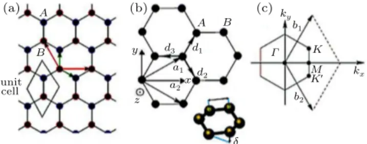
The carbon atoms in 2D graphene (contained in a plane) form a honeycomb lattice consisting of carbon atoms with sp2 hybrid covalent bonds. However, this honeycomb lattice is not of a conventional Bravais structure, since the atomic structures referring to two of the adjacent atoms are not equivalent.[1]
Figure 1(a) shows the honeycomb atomic structure of grapheme, graphene, and figure 1(b) shows a hexagonal atomic structure of Bravais (conventional). Note that the hon-eycomb structure lacks an atom located in the central part of the hexagon, so that this atomic structure cannot be consid-ered as a hexagonal atomic structure, which is a conventional Bravais structure. It is worth noting that an atomic structure can only be considered a Bravais structure when all the points
∗Project supported by the National Council for Scientific and Technological Development (CNPq).
†Corresponding author. E-mail:[email protected]
of this network are equivalent, so that the connection between any two points of the atomic structure can be obtained through the unit vectors of this network.
In the honeycomb atomic structure of graphene, its unit cell can be defined as a rhombus, where two carbon atoms are located, according to what is shown in Fig.1(a).
(a)
unit cell
(b) (c)
A
A
B
B
a
d
a a
a a d
d a
Fig. 1.(color online) (a) Unit cell related to the atomic structure of graphene (rhombus). (b) Hexagonal atomic structure. (c) Unit vectors referring to the atomic structure of graphene (a1anda2).
As we can see in Fig. 1(c), the two atoms (AandB) of the unit cell constitute two non-equivalent atoms because these two atoms cannot be connected with one or with a combina-tion of the unit vectorsa1anda2.
Since the honeycomb atomic structure of graphene can be considered as an association of two triangular atomic tures, forming a Bravais structure, in the honeycomb struc-ture of graphene, the vectorsa1anda2are the unit vectors, andd1, d2, and d3 (Fig.1(c)) are the vectors that determine the closest distances (between neighboring atoms). This dis-tance between adjacent carbon atoms (a0) has a value equal to 0.142 nm, which is the average distance between the co-valent (C–C) and double (C=C) covalent bonds that make up a graphene layer. Given that the lengths of the unit vec-tors are all given bya=√3a0, these unit vectors have length a=0.246 nm, so that
a1= √
3a0 2 ,
a0 2
! ; a2=
√ 3a0 2 ,−
a0 2
!
. (1)
Note that the three points closest to a given point in the direct graphene structure are given by
d1= a0
2
1,√3; d1= a0
2
1,−√3; d3=a0(1,0), (2)
and the six points with the second closest proximity are given by
d′1=±a1; d′2=±a2; d′3=±(a2−a1). (3) The first Brillouin zone of the graphene is presented in Fig.2, in which the unit vectors are also shown to be (|b1|= |b2|=4π/√3a)where
b1=
2π
√ 3a
2π
3a
; b2= 2π
3a0
2π
√ 3a,−
2π
3a
. (4)
The points K andK′ shown in Fig. 2 are called Dirac points, which are very important for detailing the electrical
properties of graphene, according to what will be seen later. The locations of these points in thekspace are given by
K=
2π
√ 3a,
2π
3a
; K′=
2π
√ 3a,−
2π
3a
. (5)
ky
kx
b
b
K Γ
K′
M
Fig. 2.Reciprocal structure and first Brillouin zone of graphene.
On the other hand, the silicene is constituted by a layer of atoms also forming a honeycomb atomic structure, which is obtained from the three-dimensional (3D) silicon and has sp3 hybrid covalent bonds. The electrical and optical prop-erties of silicene can be obtained from the density-functional theory (DFT). It has been proven that in the atomic structure of the silicene,B atoms of a unit cell identical to that of the graphene would need to be slightly displaced with respect to theAatoms of that unit cell. That buckled structure (Fig.3(a)) makes sense, since it is very similar to the plane (111) of the 3D silicon.[2]It is noteworthy that although the carbon and sil-icon atoms are in the same column (group 14 of the periodic table), the carbon is located in line 2 and the silicon in line 3 of this periodic table, so that these elements have different chemi-cal properties. For example, the energy difference between the valence orbitals for thesandporbitals has a value of 10.66 eV for carbon and it has a value of 5.66 eV for silicon.[3] There-fore, in the silicon atom the preference is the use of the three porbitals, resulting in sp3hybridizations.
Due to the significant increase in the silicene atomic dis-tance in relation to the graphene, theπ–π overlap in silicene decreases by roughly an order of magnitude, so that the Si=Si bonds are, in general, much weaker than C=C bonds. That is the reason why silicene has a buckled atomic structure and does not exist naturally, unlike graphene, which has a flat atomic structure.
As the bonds between silicon atoms in the silicene are a mixture of sp2and sp3hybridizations, we can state that there is no natural silicene, which means that the silicene cannot be obtained via exfoliation.[4]
sp3hybridizations occurs, the angle between the bond normal to the plane and the bonds in the buckled plane has a value of 101.73◦.[5]
The distance between neighboring silicon atoms (a0) has a value approximately equal to 0.2217 nm. As we can see from Fig.3(a), the unit cell of silicene, just as in graphene, consists of two atoms (AandB), but the unit cell of the silicene has a structure parametera≈0.384 nm. Therefore, the atomic structure of the silicene has the same properties as those pre-sented above with respect to the graphene, except that in the silicene there is a vertical displacement between the atomsA andB(δ=0.045 nm) as shown in Fig.3(b). It is noteworthy that in the 3D silicon the displacement of the atoms relative to the plane (1,1,1) is 0,078 nm.[6–8]
(a)
unit cell
(b) (c)
A
A B
B d a a d y
z
xd
ky
kx b
b K Γ
δ
K′ M
Fig. 3.(color online) Atomic structure and first Brillouin zone of silicene.
We can see from Fig. 3(c) that the first Brillouin zone for the reciprocal structure of the silicene has the same shape as the first Brillouin zone for the reciprocal structure of the graphene. Note that the locations of theKpoints are given ac-cording to Eq. (5), by changing only the value of the structure parameter.
The bonding energy between the silicon atoms in the sil-icene is 4.9 eV/atom, while in the 3D silicon (diamond-like structure) it is 0.6 eV/atom.[7]
Presently, the manner of obtaining silicene is by synthe-sizing on a substrate. Some methods have already been pre-sented, in order to obtain the synthesis of epitaxial layers of sil-icene on substrates of silver (111),[9–14]iridium (111),[14]and zirconium diboride.[15](It is obvious that the epitaxial growth consists of obtaining thin layers on crystalline substrates. We will come back to this subject further).
Possible occurrence of superconductivity in silicene on silver (111) at 35 K–40 K was also observed, which is the highest among those temperatures observed in superconduct-ing elements.[16,17]
A buckled structure of silicon atoms has also been inves-tigated and defined as Si (111), since it can be seen as a plane of Si (111).[18]
3. Energy band diagrams
It is already well known that graphene has zero band gap, which makes it difficult to use in field effect transistors. On
the other hand, silicene can behave as a semimetal with a band gap that is variable, by the application of an external electric field, or as a metal.[19–22]
Like the case of graphene, the energy bandsπ andπ∗of the silicene energy dispersion relation touch the DiracKpoint and have a linear relationship in the vicinity of that point. That dispersion relations of graphene and silicene can be calculated by means of the DFT[23]as shown in Fig.4.
-20 -10
-6 -2 2 6
En
e
rg
y
/
e
V
En
e
rg
y
/
e
V
0 10 20
K M K K G M K
σ*
σ*
σ σ
σ σ*
π*
π*
π π
Γ
(a) (b)
Fig. 4. (color online) (a) Energy band structure of graphene. (b) Energy band structure of silicene.
Graphene and silicene are referred to as “intrinsic” (with-out doping), when the Fermi energy (whose value is approx-imately equal to the chemical potential) at Dirac points has zero value. Indeed, we can hardly find, for example, intrinsic graphene, since small spatial heterogeneities always occur. On the other hand, these two 2D metamaterials (graphene and sil-icene) are called “extrinsic” (doped), when electrons are intro-duced into the conduction band (or holes in the valence band), such as through gate voltage, according to what we will see more ahead.
In intrinsic graphene and silicene, for low energy levels around the Dirac point (K), the dispersion relation is linear and can be expressed mathematically through E(q) =±VFℏ|q|, where the symbol+represents the conduction band and the symbol−refers to the valence band,q=k−K=qq2
x+q2y is the wave vector with respect to the Dirac point andVF= 106 m/s is Fermi velocity on graphene. This linear relation is valid until energy values related to the visible light, so that the frequencies used in telecommunication are also included. Therefore, graphene and silicene in their original states (with-out doping) have Fermi energyEF=0 atKpoints of the Bril-louin zone (Dirac points), where the valence band is com-pletely filled, while the conduction band is comcom-pletely empty, and the conduction and valence bands touch theKpoints. Al-though this property is very useful in many applications, it is an obstacle to the use of graphene in nanoelectronic devices, such as FETs, for example. This is because it is very difficult to open a band gap in the graphene dispersion relation, while preserving its electronic properties, given that its atomic struc-ture is completely contained in a plane.
atomic structures, which provide a difference in energy be-tween the electrons located in these two superstructures (∆). Consequently, the band gap caused at the Dirac point (K) is given byEgs=2∆. Considering that in this case the Van der Waals interactions are weak, the value of∆ is small, which implies a small value for the band gap. It is worth mentioning that the value of this band gap can be increased by changing the interaction between the two substrates, or by means of the gate voltage.
In the case of the application of a gate voltage, the open energy range (Eg) increases linearly with the increase in the value of the perpendicular applied electric field (E⊥), accord-ing to what can be demonstrated by the density theory (DFT). This occurs due to the fact that this applied electric field causes the symmetry to break between the substructures of the sil-icene (AandB), which causes a band gap to be opened. The total band gap value is the sum ofEg+Egs. However, taking into account that theEgsvalue for silicene on h-BN (substrate used will be presented below) is very small, we neglectEgs.
Note that the band gap (Eg=eE⊥δ, whereeis the charge of the electron andδ≈0.044 nm is the vertical displacement between the silicene atomic substructures) increases linearly with the increase ofE⊥.[23]
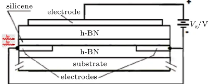
Considering the operation of an electric field perpendic-ular to the plane of the silicene, we can represent the band structure in the vicinity of theKpoint for the device shown in Fig.5, according to the following equation:[24]
E=± q
E2
g+ (ℏVFq)2, (6)
whereℏis the reduced Planck constant,VF=1.3×10⁶m/s is the Fermi velocity in silicene andq=qq2
x+q2y is the wave number aroundK.
silicene
electrode
V g/V
electrodes h-BN
h-BN substrate
Fig. 5.(color online) Schematic representation of a silicene-based field effect transistor.
Since the device shown above is a waveguide (which can be controlled via gate voltage), the photons incident on the nanoribbon are coupled to the surface plasmons (SPs) modes, forming what is called surface plasmons polaritons (SPPs).
Recent experiments were carried out with the objective of investigating the process of coupling of radiation emitted by a transmitter located above to the plane of a graphene ribbon (distanced=50 nm) and to the side, i.e., in the same plane (distanced =50 nm) of a graphene ribbon. It is noteworthy that the emitted radiation coupled with the plasmons on the
surface of graphene forming GSPPs.[25]In these experiments, the emitter was considered as an electric dipole and the thick-ness of graphene was assumed to be 0.5 nm. The coupling efficiency was defined as the ratio between the decay rate of total energy emitted by the optical source and the decay rate of energy emitted by the optical source that is transformed in GSPPs, that is, the greater the coupling efficiency, the greater the amount of energy coming from the optical source that is transformed into GSPPs, so that the smaller the dissipation loss is. It was verified (theoretically and numerically) that the coupling efficiencies in the two cases both depend on the po-larization direction of the emitted light and that the decay rate of the optical source to form GSPPs when the emitting opti-cal source is located in the same plane of the graphene is 10 times greater than that when this source is located above the graphene plane.[25]
The width of the nanoribbon strongly influences the be-haviors of the propagating modes. Briefly, the smaller the width of the nanoribbon (W), the smaller the number of modes present in the waveguide. Previous studies have revealed that in a graphene nanoribbon with width less than 50 nm, there is a single propagating mode (fundamental mode).[26] How-ever, whenW <10 nm, finite-size effects become important, so that the classical theory of local electromagnetism can no longer determine the behavior of GSPPs.[27]
In fact, unlike what occurs in conventional waveguides, where the waveguide width is given byλ/2, the GSPP modes that can propagate in a homogeneous graphene nanoribbon with a given width are determined by quite a different math-ematical formulation based among other parameters, on the width of the nanowire.[26] We adopted the width of the nanoribbonW =25 nm.
We can find the length of the nanoribbon as a function of the propagation length in which a GSPP mode undergoes energy decay in the form of (1−1/e) from its initial en-ergy. However, there are other factors that influence the length calculation, such as dispersions and non-linear effects. We adopted the length of the nanowireL=250 nm.[28]
Taking into account that we will present the detailing re-ferring to the opening of a band gap for a layer of silicene, we use a layer of silicene in the device shown in Fig.5.
The thickness of the h-BN layer was adopted as d = 12 nm, according to what will be detailed below. The h-BN layer located below the silicene layer is supported by an SiO2 substrate with a thickness of 300 nm, which in turn is sup-ported by a silicon substrate.
following Fig.6.
-2.0 -1.0 0 1.0 2.0
-1.5 -1.0 -0.5 0 0.5
Vg=0 V Vg=20 V Vg=40 V Vg=60 V
1.0 1.5
-2 0 2
-0.2 -0.1 0 0.1 0.2
q/k֓K/108
q/k֓K/109
E
/
e
V
E
/
e
V
Fig. 6.Energy versus wave vector near theKpoint.
Graphene nanoribbons can tolerate electric current den-sity greater than 108A/cm2, for widths less than 16 nm. This breaking current density has a reciprocal relationship to the re-sistivity of graphene nanofite. Joule heating is the most likely mechanism of breaking.[30]
On the other hand, the atomic structure of the silicene is preserved untilE⊥=2.6 V/ ˚A.[31]
Figure6shows the variations of energy (in unit eV) of the modes present in the silicene nanoribbon with wave number.
The range of values of wave numbers was selected in or-der to allow propagation of SPP modes up to the frequency range used in optical telecommunications. Note the existence of the gaps, according to what was mentioned above.
It is worth noting that in the absence of the electric field, the dispersion relations of silicene and graphene are similar (E=ℏVF|q|), with small deviations in the values, due to the fact that the Fermi velocity in the silicene is slightly higher than in the graphene, according to what was mentioned previ-ously.
4. Substrates
A graphene nanoribbon has roughness due to several fac-tors. Then, the substrate on which the graphene nanoribbon is supported must conform to the roughness, i.e., graphene after transferring, must be free of wrinkles or distortions. Thermal deposition of SiO2generally results in high surface roughness. In addition, graphene on SiO2 does not show charge homo-geneity along its surface.
On the other hand, hexagonal boron nitride (h-BN), termed white graphite, is also contained in a plane. This mate-rial is an isomorphic graphite, in which the boron and nitrogen atoms are located at pointsA andBof the graphene atomic structure. Therefore, the atomic structure of h-BN is similar to the atomic structure of graphene. The space between two lay-ers of graphite is 0.355 nm and the space between two laylay-ers of h-BN is 0.333 nm.[32]
Since the roughness of the surface of the h-BN layer is much smaller than the roughness of the SiO2surface, the graphene nanoribbon is much better positioned on the surface of h-BN.
There are several methods of depositing f h-BN layers on the SiO2/Si. However, despite the similarity between those two materials, graphene can be considered as a semiconductor with zero bandgap, while h-BN is considered as an insulator, whose bandgap has a value equal to 5.9 eV.[33]
Graphene and h-BN have very strong covalent bonds in the plane, and weak Van der Waals bonds between adjacent planes. However, the atomic bonds in the h-BN are approx-imately ionic, when compared with the atomic bonds of the graphene.[34]
Considering the fact that the roughness of h-BN is much smaller than the roughness of SiO2, graphene embedded be-tween layers of h-BN has charge mobility and charge ho-mogeinity with values that are almost an order of magnitude higher than those embedded between layers of SiO2. From the Drude formula it was determined that the charge mobility for graphene supported by h-BN varies from 2.5×104 cm2/V·s at high charge density(in agreement with the Hall mobility) to 1.4×105cm2/V·s near the charge neutrality point.[35]Hence, we determine the value of the charge mobility on graphene over h-BN to beµ=2.5×104cm2/V·s at high charge densi-ties.
The graphene (or silicene) layer in our device is embed-ded between two layers of h-BN, the h-BN layer being located below the graphene (or silicene) and it is supported on a sub-strate consisting of SiO2, which in turn is supported on a sili-con substrate. The thickness of the h-BN layer located above the graphene (or silicene) layer should be≈>10 nm in or-der to smooth the roughness of the SiO2layer, as well as to prevent the graphene layer from receiving unwanted charge carriers. On the other hand, the thickness of this layer of h-BN must be≈<70 nm, to assure the operation of the gate voltage applied to the graphene (or to the silicene).
Mechanical exfoliation method of making graphene, which is actually contained in a plane, does not work for sil-icene. So far, the main method of synthesizing silicene is by means of epitaxial growth.
Ag (111)[38–40]and√3×√3) (relative to the structure of the silicene (1×1)).[38,41,42] The reason forchoosing silver as a substrate for the growth of the silicene is due to the fact that this material provides a moderate and homogeneous interac-tion with the silicene, which results in very moderate tensions in the silicene in the process of growth.[43]
In the superstructure (4×4), the silicene sheet is posi-tioned on the surface of Ag (111), so that a supercell (3×3) of the silicene coincides with a supercell (4×4) of Ag (111).
The superstructure (4×4) is called “magic incompatibil-ity”, which is due to the fact that we can consider the silver structure parameter (is) as aAg=0.288 nm and the silicene structure parameter (is) asaSi=0.384 nm, which gives the ratio 4×aAg=3×aSi. Note that the two atomic structures (Ag (111) and silicene) are hexagonal. Consequently, the in-terference between the two superstructures is minimal, which provides the stabilization of the atomic structure of the sil-icene, according to what is shown in Fig.7.[44,45]
(a) (b)
(c)
Si on Ag Ag (111)
Fig. 7.(a) Schematic representation referring to the 3×3 superstructure of the isolated silicene. (b) Schematic representation of the 4×4 superstructure of the Ag (111) surface. (c) Schematic representation of the superstructure (4×4)−α.
The 4×4 superstructure can be obtained by placing a sil-icene (1×1) structure on the Ag (111)-1×1 structure. How-ever, since the silicene atomic structure does not completely coincide with the atomic structure of silver (111), the silicene atoms are located between, or above, the Ag atoms (Fig.7).
We can state that from the structure parameter of the sil-icon unit cell (a≈0.384 nm), it is easy to find the distance between neighboring silicon atoms (≈0.2217 nm). Note that the covalent radius is≈0.11085 nm. Recall that in 3D silicon the atomic radius is 0.118 nm. On the other hand, the atomic radius of the silver atom isrAg=0.144 nm and the silver (111) structure parameter isaAg=0.288 nm.
The 3×3 superstructure of the silicene is shown in Fig.7(a), and the 4×4 superstructure related to Ag (111) is shown in Fig.7(b). Figure7(c)represents the overlap of the
3×3 superstructure of the silicene on the 4×4 superstructure of Ag (111).
Since the covalent radius of the silicon atom in the icene (solid lines) is smaller than the atomic radius of the sil-ver atom (dash lines), it is not possible to place silicon atoms forming a hexagon, tangent to the silver atoms in accordance with what can be observed in the detail inserted in Fig.7(c).
The scanning tunneling microscope (STM) image shows that in the Si (3×3) superstructure on Ag (4×4) superstruc-ture there are six protrusions in each unit (due to the higher atoms of the silicene), which does not happen in the Moir´e pattern. Given that in the 3×3 superstructure of silicene there are 18 silicon atoms, half of these atoms would be at the high-est level and the other half at the lower level. However, when the silicene is placed on the surface of the substrate consti-tuted by Ag (111), the buckled structure of silicene causes the energy surface to lower. Then, due to this energy reorganiza-tion, there are only 6 silicene atoms at the highest positions and 12 silicene atoms at the lower positions of the Si (3×3) superstructure[40,46]as shown in Fig.7(c).[44]
Note that three of the six silicene atoms located at the up-per level of this 3×3 superstructure belong to one half of the superstructure and the other three silicene atoms belong to the other half of that superstructure. The highlighted circles in Fig.7(c)represent the atoms located at the highest level.
The configuration of this Si (3×3) superstructure on Ag (4×4) superstructure is called a 4×4–α phase.[40] In the 4×4–α phase, the six higher atoms do not belong to the same atomic substructure of the silicene (it is unlikely to happen in the isolated silicene, in which all the higher sili-con atoms belong to the same atomic substructure and all the lower atoms belong to the other atomic substructure). Fur-thermore, the 4×4–α phase is not located on the edges of the silicene sheet. On these edges there is another configura-tion called a 4×4–β phase. The configurations of these two phases are different, probably due to the fact that the phase (4×4–β) is less stable than the other phase (4×4–α), but the stresses that emerge at the ends of the silicene sheet help stabilize the silicene atoms.[46]In addition to the Si (3×3) su-perstructure on Ag (4×4) superstructure detailed above, there are four other configurations (phases) of possible superstruc-tures relating to the silicene on Ag (111), depending on the temperature to which the substrate is subjected.
For temperatures below 400 K, the silicon atoms de-posited on the surface of Ag (111) tend to form disordered atomic structures.[47]However, for temperatures above 400 K during the deposition of the silicon atoms, the obtained sil-icene sheet exhibits the superstructure phases 4×4, √13× √
13 R13.9◦,√7×√7 R19.1◦, 2√3×2√3 R30◦, and√3× √
direct deposition of silicon atoms and annealing at 670 K, including the surfaces of Ag (111), zirconium diboride– ZrB2(0001),[15]and iridium Ir (111).[48]
A highly wrinkled sheet of silicene was fabricated on a molybdenum disulfide (MoS2) semiconductor substrate, which represents the possibility of obtaining an isolated sheet of silicene, thus avoiding the influence of the metal substrate on the electronic structure of the silicene.[49]
In addition, multilayer silicene sheets were manufactured on Ag (111) surfaces by using epitaxial technology.[39,50–55]
Since the surface of the silicene is chemically active, chemical adsorbents can be used, which can change the electri-cal/optical properties of the silicene, such as a band gap open-ing and its transformation into semiconductor.[56–61]
Since the interaction between the graphene or silicene and the substrate can change their electronic properties, these 2D metamaterials acting on a nanoelectronic device need to be placed on insulating substrates. Therefore, the choice of the insulating substrate where the graphene or the silicene is sup-ported could bring benefits to the nanoelectronic device based on graphene or silicene.
The manufacture of a silicene-based electronic device is more difficult than that of a graphene-based electronic de-vice,for the transferred silicene in the air is unstable. Hence, the transfer of the silicene via the transfer technique widely used in graphene cannot be used for silicene. However, recent research has shown a method of transferring this 2D metama-terial to a substrate.[62]First, the silicene was synthesized by epitaxial growth on Ag (111) and a thin layer (5 nm) of alu-mina (Al2O3)was added on the silicene. After this step the silicene together with the Ag (111) were rotated at an angle of 180◦and deposited on a layer of SiO2. In this way, the silicene layer was preserved during its transfer and it was possible to manufacture an FET. To complement the manufacture of this FET, part of the Ag (111) layer was removed, so that the re-maining parts of this material serve as contacts (source/drain). In the same way that has already been detailed for graphene, we focus on more detail of the silicene on h-BN. The cohesion energy between the silicene and the h-BN sub-strate is approximately 0.07 eV to 0.09 eV per atom of silicon, while between the silicene and the metal surface it is 0.5 eV per atom of silicon.[63]
Considering the fact that the cohesive energy between the silicene layer and the silver surface is very high, there are misgivings that the strong energy interaction between these two surfaces can strongly influence the structure of the en-ergy band on the surface of the silicene. In addition, this strong interaction may be sufficient to cause the Dirac cone related to the silicene on Ag (111) to disappear. On the other hand, the weak Van der Waals interactions between the sil-icene and the h-BN do not affect the electrical/optical prop-erties of the silicene. Therefore, due to the wide bandgap of
h-BN, the silicene should behave as being almost isolated (in-cluding the Dirac cone), in superstructures made of silicene on h-BN.[63–65]
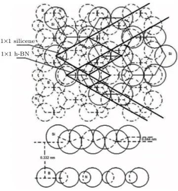
The upper part of Fig.8shows the graphical representa-tion of the overlaying of the silicene layer on h-BN.
1T1 silicene
1T1 h-BN
Fig. 8.Top: Atomic structure of silicene on h-BN forming a superstructure. Bottom: Transverse section of the silicene atomic structure on h-BN.
The circles in solid lines represent the atoms of the atomic structure of the silicene, which are positioned on the atomic structure of h-BN, whose circles which are drawn in dash lines represent the atoms of h-BN.
Note that the diamonds represent a unit cell for the sil-icene and a unit cell for h-BN respectively. The right position-ing of the atoms provides the alignment between the atomic structures of the silicene and the h-BN, as we can see in the upper part of Fig.8.
According to the above-mentioned, while the h-BN atoms are spaced by 0.144 nm and the h-BN structure parameter is 0.25 nm, the minimum distance between the atoms of the silicene is 0.2217 nm and the silicene structure parameter is 0.384 nm.
The interactions between these two atomic structures pro-vide the opening of a band gap at the Dirac points (K) of the silicene, whose value is approximately 30 meV, which does not depend on the rotation between the alignments of the struc-tures of the h-BN and silicene.[64]It is important to state that the bandgap value is caused by the distance between the layers of silicene and h-BN, whose value is 0.332 nm, according to what can be seen in the lower part of Fig.8.[63,66]
The dispersion relation of the silicene on h-BN in the vicinity of the Fermi level can be found by the tight-binding
model according to Eq. (6), that is,E(k) =±q∆2+ℏ2V2 Fk2, where∆is the energy difference between the electrons located in the two superstructures. Consequently, the band gap caused at theK point is given byEg=2∆. Considering the fact that the Van der Waals interaction is weak, the value of∆ is small, which implies a small value for the band gap. It is worth men-tioning that the value of this band gap can be increased by changing the interaction between the two substrates, or by ap-plying a gate voltage. Note that the control of the band gap value via gate voltage has already been detailed above.
Besides the h-BN, some other insulating material can act as substrate to support graphene and silicene, preserving its necessary physical characteristics, so that they can consti-tute future efficient optoelectronic nanodevices. For example, graphene can be obtained from silicon carbide (SiC) via high temperature treatment (HTT), with the advantage that thermal decomposition is a relatively simple process and can be per-formed over a wide temperature range (1400 K∼2000 K), under a high or medium vacuum.[67]
Silicon carbide crystal structure has polytypism, i.e., sil-icon carbide exists in about 250 crystalline forms.[68]Indeed, the polymorphism of SiC has a large family of similar crys-talline structures (polytypes), which can be described by a usual hexagonal axis system, with one c-axis perpendicular to three equivalent axesa,b, andd having angles 120◦with one another. All crystallographic modifications have very sim-ilar structures, which consist of identical layers perpendicu-lar to the hexagonal or trigonal axes. The (0001) (silicon-terminated) or (000-1) (carbon-(silicon-terminated) faces of 4H–SiC and 6H–SiC wafers can be used for growing the graphene.[69] Graphene growth on SiC can be done in a variety of ways, for example, in flat SiC surfaces,[70,71]SiC structured surfaces,[72] and discrete SiC particles.[73] It is noteworthy that after the growing graphene on SiC, the SiC that has been used can serve as a substrate for manufacturing the elec-tronic graphene/SiC devices, thereby avoiding assemblying and/or transferring the graphene films to the SiC used by graphene production methods via mechanical exfoliation, for example.[74,75]
With respect to the silicene, it has been proven that the semi-metallic behavior of silicene embedded in ultra-thin lay-ers of aluminum nitride (AIN), which is considered as an insu-lating (energy gap about 4.6 eV), can be preserved.[76]In this case, the thin layer of silicene interacts very weakly with the AIN layer through van der Waals (vdW) force.
Partial charge densities in the energy range ofEF/EF− 0.2 eV of silicene on h-BN and of silicene on hydrogenated Si-terminated silicene carbide SiC (0001) surface (Si–SiC) are concentrated on silicene (in the same way as that in free-standing silicene). However, partial charge densities related
to silicene on hydrogenated C-terminated silicene carbide SiC (0001) surface (C–SiC) are distributed widely in silicene and substrate, so that in this case,EFapproaches to the maxi-mum value of the C–SiC valence band. Therefore, silicene on hydrogenated Si-terminated silicene carbide SiC (0001) sur-face (Si–SiC) maintains the Dirac cone, and its geometry and electronic properties are preserved. On the other hand, silicene on hydrogenated C-terminated silicene carbide SiC (0001) sur-face (C–SiC) has metallic behavior.[77]
Molybdenite, i.e., MoS2 is a transition metal dichalco-genide (TMD) that classifies as a material of van der Waals. While the band gap of bulk MoS2is 1.29 eV, and the band gap of MoS2monolayer is 1.90 eV.[78]
Previous studies have shown that the energy conver-sion energy efficiency of photovoltaic cells based on Schot-tky diode is significantly increased, when an MoS2 layer is inserted into the junction region (contacting graphene) be-tween the graphene layer (in the case of trilayer-graphene) and the n-Si layer. The photovoltaic cell constituted by Indium electrode/n-Si substrate/SiO2 layer/MoS2 layer (≈ 9 nm)/trilayer-graphene/Au electrode presented an energy conversion efficiency of 11.1%. The correct determination of the thickness of the MoS2layer contributes significantly to the increase of the energy conversion efficiency. This is because the MoS2layer separates the graphene from the n-Si substrate, which penetrates through a hole in the SiO2layer until it en-counters the MoS2layer. Considering that the MoS2layer acts as a charge recombination reducer at the junction, the opti-cal loss decreases, thus increasing the energy conversion ef-ficiency. Another reason that contributes to the increase of the energy conversion efficiency related to this nanophotonics photovoltaic cell is the correct determination of the number of layers of graphene (in this case trilayer-graphene), since this number of graphene layers can reduce the value of the Schot-tky diode resistance.[79]
There are two forms of silicene/MoS2 heterostruc-tures: high-buckled silicene (HSMS) and low-buckled silicene (LSMS). In both formats, the covalent bonds of the silicene are maintained (without breaking). However the HSMS for-mat presents metallic behavior, unlike what happens in the LSMS format, which is more stable and its band gap can be controlled by gate voltage, in the same way as that in the case of silicene/h-BN.
5. Charge mobilities and charge densities
Previous studies have demonstraded that the isolated graphene has a charge carrier mobility value of 2× 105cm2·V−1·s−1at room temperature.[82,83] However, more recent studies have shown that the mobility of the isolated graphene is 3.39×105 cm2·V−1·s−1 for electrons and it is 3.22×105cm2·V−1·s−1for holes at room temperature.[84]On the other hand, the mobility of graphene over SiO2 is only 10×103cm2·V−1·s−1 [85]and the value of the charge mobility of graphene on h-BN isµ=2.5×104 cm2·V−1·s−1at high charge densities.[35]
With respect to silicene, recent research has shown that the isolated silicene has an electron mobility of 2.57×105 cm2·V−1·s−1 and a hole molibity of 2.22× 105cm2·V−1·s−1at room temperature.[85]
In the same way as that in the case of graphene, the mo-bility of the charge carriers in the silicene depends greatly on the substrate where it is embedded, and the h-BN is one of the substrates which offers a relatively high mobility for the silicene.[45]
The symmetric shapes of the energy dispersion relation in graphene for the conduction and valence bands provide equal group velocity for electrons and holes. In other words, con-sidering ideal graphene (without defects and impurities), or isotropic scattering graphene, that is, when scattering mecha-nisms affect electrons and holes with the same intensities, the average velocity of the charge due to the presence of an elec-tric field (Vdrift)is the same for electrons and holes. Then, in ideal graphene, the mobility of electrons (µe)is equal to the mobility of holes (µh).
The charge mobility can be determined from the mea-surement of resistivity in a high charge density regime (called metallic regime), where the induced charges do not change the resistivity significantly, according to the following equation:
µe,l= 1
enρ, (7)
whereρis the electrical resistivity of graphene.
The density of charge carriers for intrinsic graphene is
given byn0= q
(n∗/2)2
+n2th≈0.3×1012cm−2, wheren this the contribution due to the generation of charge carriers at the due temperature andn∗is the contribution due to the charges coming from the substrate.
The application of a gate voltage provides an increase in charge density, owing to the fact that graphene (or sil-icene) and the dielectric substrate form a capacitor (whose capacitance is constituted by the quantum capacitance of the graphene, in series with the capacitance referring to elec-trode, dielectric and graphene). For the device we are present-ing, the quantum capacitance of graphene (or silicene) can be neglected,[86]so that the contribution to the charge density due to the application of gate voltage (ng), without taking into ac-count the unbalanced loads due to imperfections, among other factors, is given by
ng=
ε0εVg
te , (8)
wheretis the thickness of the dielectric.
However, taking into account the ambient temperature (T =300 K), which causes the value ofKBT ≈26 meV and the chemical potential of the graphene µq≈EF≫KBT, the application of gate voltage provides a great change in the total charge density in graphene, given by[26]
n=µ 2 q ℏ2·
1
πV2 F
, (9)
whereℏis the reduced Planck constant.
For example, considering the Eq. (7) and using µq= 0.5 eV we obtainn=1.837×1013cm−2.
It is noteworthy that the chemical potential of graphene is given by[87]
µc=ℏVF√nπ. (10) Moreover, the value of the gate voltage (Vg)is related to the Fermi level (the value is approximately the same as the value of the chemical potential), according to the following equation[88]
EF∼=µq=ℏVF r
πε0εd
VD =4.5 V. (Please, replace this text: Then, we adopted VD=4.5 V.)
On the other hand, the concentration of charges in a range of energy (in this case, referring to the device shown in Fig.5) can be obtained by integrating the Fermi–Dirac dis-tribution function over the energy band. Hence the concen-tration of charges is given by n=R
D(E)fF(E)dE, where D(E)and fF= 1+e(E−Ef)/(KBT)−
1
are the available energy states (density of states (DOS)) and the distribution function of Fermi–Dirac, respectively.
After several mathematical interventions, the total con-centration of electrons in the silicene can be determined from[91]
n= 2W L πℏ2V2
F h
∆Γ(1)KBT I0(η) +Γ(2) (KBT)2I1(η) i
, (12)
whereW andL are the width and the length of the silicene nanoribbon, respectively,η= (EF−∆)/KBT,Γ,KB,T, and Iibeing the gamma function, the Boltzmann constant, the tem-perature, and the Fermi–Dirac integral, respectively.
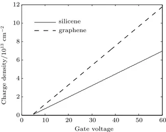
Figure 9shows the charge densities in graphene and in silicene as a function of gate voltage ranging from 5 V to 60 V (Efranging from 0.1965 eV to 1.2743 eV) .
0 10 20 30 40 50 60
0 2 4 6 8 10 12
Gate voltage silicene
graphene
Ch
a
rg
e
d
e
n
si
ty
/
1
0
1
3 c
m
-2
Fig. 9.Charge densities on graphene and silicene as a function of gate voltage.
For high values ofVg(which lead to high values of the chemical potential (µq≈Ef)), ∆ ≪Ef. In this case, equa-tion (12) becomes Eq. (9), considering the Fermi velocity for the silicene.
In Fig.9it is shown that the charge densities in graphene (Eq. (9)) and in silicene (Eqs. (9) and (12)) as a function of gate voltage (ranging from 5 V to 60 V, which causesEf to vary from 0.1965 eV to 1.2743 eV).
As we can see from Fig. 9, the charge densities in graphene and in silicene increase linearly with the increase in the gate voltage, but in graphene the charge density is slightly higher than in silicene due to the fact that the Fermi velocity in graphene is slightly higher than in silicene.
6. Conductivities and absorptions
Graphene and silicene in their original states (without doping) have Fermi energyEF=0 at theKpoints of the Bril-louin zone (Dirac points), where the valence band is com-pletely filled while the conduction band is comcom-pletely empty. The conduction and valence bands touch theKpoints, andnear these points the dispersion relation can be considered to be lin-ear. In this case, the optical excitations cause electron-hole ex-citations, called intraband and interband transition, according to what is shown in Fig.10.
valence band condution band
intraband transition Fermi energy
level
interband
transition k
K
Fig. 10.Schematic representation of intraband and interband transitions.
Hence, the optical conductivities of graphene and silicene are determined by intraband and interband transitions, which can be obtained from the Drude model,[92]given by[93–95]
σ(w) =σDC(EF)/(1+w2τ2), (13)
whereσDC is the direct current (DC) conductivity and w is the angular frequency of the incident photon, andτis the re-laxation time (period of time in which an electron can move freely after its previous collision).
Actually, the conductivities of graphene and silicene are the sum of the contributions referring to the intraband and in-terband excitations, which can be calculated using the Kubo formula. Considering that we are dealing with angular fre-quenciesw≫1/τ, i.e.,βF<w→neff<c/VF≈300, where neffis the effective refractive index (neff=β/0;k0=2πλ0),β is the wave number for the GSPP mode,λ0is the wavelength of the photon in free space andcis the speed of light in the vacuum; under these conditions the intraband conductivity of graphene is given by[87,96,97]
σintra(w,µc) =
ie2µc
(ω+iτ−1)πℏ2, (14)
where the relaxation time (τ) is given by[26,98]
τ=µcµ
eVF2 (15)
and the interband conductivity of graphene is given by[87,96]
σinter= e2 4ℏ
"
1+ i πln
ℏ ω+iτ−1 −2µc
ℏ(ω+iτ−1) +2µ c
#
For high frequencies (w≫µc,KBT), the conductivity of graphene is given byσ0=e2/(4ℏ)≈6.08×10−5 Ω−1=> 0,[87] σ0 being defined as the universal conductivity of graphene, which can also be represented byσ0=π0/4, where G0=2e2/his what is called quantum of conductance.[99]
In Fig.11we show the graphs of the real (left part) and imaginary (right part) referring to the intraband, interband, and total, of the graphene embedded in h-BN, as a function of 0≤µc≤1 (eV), for λ =1.5317024 µm, which belongs
to theCband of Telecommunication Standardization Sector -ITU (on the top of Fig.11) and for frequency f =10 THz (on the bottom of Fig.11).
0 0.5 1.0 0 2 4 6 8 Chemical potential/eV R e a l p a rt / 1 0
-5 S
intra inter total
0 0.5 1.0 -1 0 1 Chemical potential/eV Im a g in a ry p a rt / 1 0 -4 S
0 0.5 1.0 0 2 4 6 Chemical potential/eV R e a l p a rt / 1 0 -5
S intrainter
total
0 0.5 1.0 -1 0 1 2 Chemical potential/eV Ima g in a ry p a rt / 1 0 -3 S
Fig. 11. Upper: Conductivity of graphene embedded in h-BN forλ= 1.5317024µm. Bottom: Conductivity of graphene embedded in h-BN for
f=10 THz.
Note that for λ =1.5317024µm, the total real part of the
graphene conductivity (solid line) is provided by the real part of the interband conductivity (dash line), while forf=10 THz (λ =30µm), the total real part of the graphene conductivity
is provided by the real part of the intraband conductivity (dash and dotted line). In addition, forλ =1.5317024µm, the total
imaginary part of the graphene conductivity (solid line) is ob-tained by the sum of the imaginary parts of the intraband (dash and dotted line) and interband (dash line) of the graphene con-ductivity. In this case, the total imaginary part of the graphene conductivity can be negative or positive. On the other hand, for f =10 THz, the total imaginary part of the graphene conduc-tivity is provided by the imaginary part of the intraband con-tribution. In this case, the total imaginary part of the graphene conductivity is positive. It is worth mentioning that for a pos-itive value of the imaginary part of the conductivity, graphene (and silicene) can support TM modes. (Considering the fact thatxis in the direction of propagation, TM modes have elec-tromagnetic fields componentsHy,Ex, andEz). We will return to this subject in the next section.
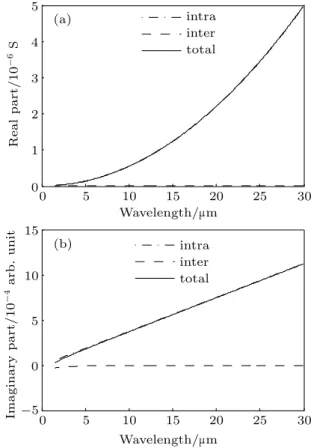
In Fig.12 are shown the graphs of the real and imagi-nary parts of the graphene conductivity embedded in h-BN, as a function of wavelength ranging from λ =1.55 µm to λ=30µm, forµc=0.6 eV.
As we can see, the imaginary part of the conductivity of graphene is positive over the entire wavelength range.
It is important to state that the universal conductivity shown for graphene is also valid for the chemical elements Si, Ge, and Sn of group IV of the periodic table, constituting a plane (or semiplane) with honeycomb atomic structure.
0 5 10 15 20 25 30
0 1 2 3 4 5 R e a l p a rt / 1 0 -6 S intra inter (a) (b) total
0 5 10 15 20 25 30
-5 0 5 10 15
Wavelength/mm
Wavelength/mm
Ima g in a ry p a rt / 1 0 -4 a rb . u n it intra inter total
Fig. 12.Real and imaginary parts of the conductivity of graphene em-bedded in h-BN versus wavelength (µc=0.6 eV).
The complex conductivities of graphene and silicene can also be obtained from their complex permittivities. The real part of the silicene conductivity, for example, can be found through the Ehrenreich–Cohen formula, and the imag-inary part of that conductivity from the equation of the real part, via Kramers–Kronig relations concerning the dielectric functions.[100,101] However, by applying the correct values with respect to the physical properties of the silicene, for wavelengths between the THz and infrared frequency region, we can use Eqs. (14)–(16) for determining the real and imagi-nary parts of the silicene .
imaginary part of the conductivity of the graphene and silicene are practically the same.
For a layer of graphene (or silicene) under the normal incidence of electromagnetic waves, the absorption at ω > 2µc/ℏ is given by A=παs/(1+παs)2≈παs ≈2,293%, where αs = e2/(4πε0ℏc) is the Sommerfeld finestructure constant.[100] This means that universal absorption occurs whenλ <πcℏ/µc. On the top of Fig. 13are shown the re-gions of the wavelengths where universal and non-universal absorption occur, as a function of the chemical potential.
0 0.2 0.4 0.6 0.8 1.0 0
20 40 60 80 100 120 140
non-universal absortion
U.A.
Chemical potential/eV
W
a
v
e
le
n
g
th
/
m
m
0 5 10 15 20 25 30
0 0.005 0.010 0.015 0.020 0.025
chemical potential: 0.15 eV
Wavelength/mm
A
b
so
rp
ti
o
n
(a)
(b)
Fig. 13. (a) Range of lengths where universal and non-universal ab-sorption occurs depending on the chemical potential. (b) Abab-sorption as a function of wavelength forµc=0.15 eV.
The following equation can be used to determine the absorption values, with considering normal incidence and the graphene layer (or silicene) embedded in a single dielectric:[101]
A= Re(σ˜(ω))
1+σ˜(ω) 2
2, (17)
where ˜σ(ω) =σ(ω)/(ε0c).
Equation (17) shows the values of the absorption as a function of the wavelength (for µc=0.15 eV) in the lower part of Fig.13. Note that forλ<≈4.133µm occurs the value
of the universal absorption.
The physical explanation for what was detailed above is that absorptions occur in graphene, when an electron in the valence band absorbs a photon and is excited to an empty state in the conduction band, with the same momentum (in-terband transitions). However, the in(in-terband transition can only occurs when there is a occupied state with Dirac en-ergy ε = (−h¯ω)/2 and an empty state with Dirac energy
ε= (+h¯ω)/2. This means that the interband transition can only occurs, for µg<h¯ω/2 (“Pauli blocking mechanism”). On the other hand, the intraband transition can also lead to absorption process. This type of transition occurs due to inter-actions with phonons, but it only exists in a significant amount from the far infrared frequencies until the THz frequencies in the presence of high concentration of charge carriers. Hence, the probability of occurrence of intraband transitions tends to zero, when whenµg→0.
The absorption also depends on the angle of incidence and on the angle of refraction according to the following equa-tion (for TM modes):[100]
A= 4
√
ε1cos(θ1)Re(σ˜) √
ε1cos(θ1) +√ε2cos(θ2)
2, (18)
whereθ1andθ2are the incidence and refraction angles, re-spectively, andε1andε2are the dielectric constants of the two media in which the 2D metamaterial is embedded. Figure14 shows the absorption values (considering ε1=ε2=1) as a function of the incidence angle (ranging from 0 toπ/2 rad), referring to the incidence of violet light (λ =0.3 nm, photon energyEph≈3.1 eV).
0 0.2 0.4 0.6 0.8 1.0
0 0.1 0.2 0.3 0.4 0.5
photon energy: 3.1 eV chemical potential: 1 eV
Angle of incidence/(π/2)
A
b
so
rp
ti
o
n
0 0.2 0.4 0.6 0.8 1.0
-5 0 5 10 15
photon energy: 3.1 eV chemical potential: 1.8 eV
Angle of incidence/(π/2)
A
b
so
rp
ti
o
n
/
1
0
-6
(a)
(b)
Fig. 14.Absorption versus angle of incidence. (a)µc=1 eV. (b)µc= 1.8 eV.
Note that on the top of Fig.14is the plot of absorption versus angle of incidence for gate voltage with valueµc=1 eV (<Eph/2). We can see that for values close to the angle
π/2 rad the absorption increases to approximately 0.5. On the other hand, in the lower part of Fig.14is the plot of ab-sorption versus angle of incidence for gate voltage with value
We will come back to this subject in the next section. It is note-worthy that although we have shown the absorption as a func-tion of angle of incidence and gate voltage values (for photons in the region of violet light), the above detailed is valid for the entire frequency range, from the THz region to the ultraviolet region.
7. Electrical permitivities, wave vector
disper-sion relations, TM and TE modes
The electrical permittivity and dielectric constant for an isolated 2D metamaterial can be obtained from the Maxwell equations given by[102]
ε=ε0+i
σ
ωt; εr=1+i σ ωε0t
, (19)
respectively.
It is obvious that in this case, the refractive index n= εr)0.5is given by
n= r
1+i σ
ωε0t
. (20)
Complex refractive index of 2D metamaterial embedded in the same dielectric can be determined asn=n(ω)−ikω, wherekis called the extinction coefficient.
We can determine the behavior of the electromagnetic wave in 2D metamaterial, by using the Dyadic Green function and Maxwell’s equations and by manipulating the polarization state.[102–104]
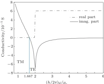
Graphene can support TE (polarizationp) or TM (polar-izations) modes, provided that the imaginary part of its con-ductivity is negative or positive, respectively (silicene behaves in a similar way to graphene according to what was previously detailed).
From Eq. (14), we can show that the real part of the in-traband contribution is null (Figs.11and12), so that only the interband contribution of the conductivity constitutes the real part value of the conductivity of the graphene (and silicene). Note that for valuesℏω/µc>2, the real part of the
conduc-tivity of the graphene (σ)is positive according to what can be seen in Fig.15.
The equation that determines the electrical permittiv-ity in 2D metamaterial already presented above is given by
ε=ε0+i(σ/(ωt)). It is important to state that considering the real and imaginary parts of the conductivity (σ=σ′+σ′′), this equation can become (from the Maxwell equations)ε= ε0−σ′′/(ωt) +i(σ′/(ωt)). Note that in this case, the real part of the permittivity for each of graphene and silicene is given by ε′=ε0−σ′′/(ωt)and the imaginary part is given byε′′=i(σ′/(ωt)). Therefore, the real parts of the permit-tivity of graphene and silicene can be positive, or negative, depending on the imaginary part of the conductivity of that 2D material. It is worth noting that when the real part of
this permittivity is negative, TM modes can exist. On the other hand, when the real part of this permittivity is posi-tive, TE modes can exist. Therefore, in graphene and in sil-icene, modes TM (ε′=ε0+σ′′/(ωt)<0;σ′′>0)or weak TE modes (ε′=ε0+σ′′/(ωt)>0;σ′′<0)can occur,[105] accord-ing to what can be seen in Fig.15. Hence, SPP modes TM and TE are supported in graphene, for 0<ℏω/µg<1.667 and 1.667<ℏω/µg<2, respectively.[106,107]
1 1.6672 3 4 5 6
-8 -6 -4 -2 0 2 4 6 8
TM
TE
↼h⊳π↽ω/µc
Co
n
d
u
c
ti
v
it
y
/
1
0
-5 S
real part imag. part
Fig. 15.(color online) Graphene conductivity as a function ofℏω/µc.
Moreover, the increase in temperature causes the real parts of the conductivity of graphene and silicene at the point of bifurcation to slightly change (where σ′=0), so that the real part of the conductivity becomes slightly positive for some values of ℏω/µg≈<2. Hence, in this case small attenua-tions occur in the SPP modes, and TE modes suffer greater attenuations.[105]
The dispersion relation for the TM mode on a sheet of graphene embedded in a dielectric can be obtained from Maxwell’s equations, given by[108]
r
q2−ω2εd c2 =−
2ωε0εd
iσ , (21)
whereqis the wave number of the GSPP modes,ω=ck0and
εdis the dielectric constant of the medium in which graphene or silicene is embedded.
From Eq. (21), we can obtain the following dispersion re-lation for TM modes:[98]
q2TM=k20 "
εd−
2εd
η0σg 2#
, (22)
whereεdis the relative permittivity of the dielectric,η0is the air impedance andη0=377Ω, andk0=2πλ0.
On the other hand, the dispersion relation for GSPPs TE mode on a graphene (or silicene) surface can be determined according to the following equation:[107]
q2TE=k02 "
εd− η
0σg 2εd
2#
The wavelength for a GSPP mode propagating through a graphene or silicene nanoribbon, and its propagation distance, i.e., the distance that this mode can propagate until its intensity decreases to 1/eof its value, are given by[109–112]
λGSPP= 2π
Re[q]; LpGSPP = 1
2 Im[q]. (24)
8. Conclusions
The 2D metamaterial (in which atoms constitute a plane or a semi-plane) is considered to be of great relevance to the progress in all exact sciences. Since the discovery of graphene, researchers around the world have increasingly investigated in depth the details of the electrical/optical properties relat-ing to the other two-dimensional (2D) metamaterials, such as silicene. The huge interest in silicene occurs due to the usage of silicon in the optoelectronic industry. Note that the constant advance in the technology related to the silicene allows us to inform that it will most probably be possible to find the solu-tion to enable Moore’s law in dimensions smaller than 10 nm. In this review, we include the details and comparisons of the atomic structures, diagrams of energy bands, substrates, charge densities, charge mobilities, conductivities, absorp-tions, electrical permittivities, dispersion relations of the wave vectors and supported electromagnetic modes referring to the graphene and to the silicene. Hence, we have developed the subjects most relevant to the professional life of those who work in the area of nanotechnoly and nanophotonics based in graphene or silicene.
References
[1] Ozawa E, Kroto H W, Fowler P W and Wassermann E1993Phil. Trans. R. Soc. A3431
[2] Takeda K and Shiraishi K,1994Phys. Rev. B5014916
[3] Lalmi B, Oughaddou H, Enriquez H, Kara A, Vizzini S, Ealet B and Aufray B2010Appl. Phys. Lett.97223109
[4] Aufray B, Kara A, Vizzini S, Oughaddou H, Leandri C, Ealet B and Le Lay G2010Appl. Phys. Lett.96183102
[5] Liu C, Feng W and Yao Y2011Phys. Rev. Lett.107076802 [6] Takeda K and Shiraishi K1994Phys. Rev. B5014916 [7] Durgun E, Tongay S and Ciraci S2005Phys. Rev. B72075420 [8] Cahangirov S, Topsakal M, Akt¨urk E, Ahin H S and Ciraci S2009
Phys. Rev. Lett.102236804
[9] Vogt P, De Padova P, Quaresima C, Avila J, Frantzeskakis E, Asensio M C, Resta A, Ealet B and Le Lay G2012Phys. Rev. Lett.108155501 [10] Jamgotchian H, Colignon Y, Hamzaoui N, Ealet B, Hoarau J, Aufray B
and Bib´erian J2012J. Phys.: Condens. Matter24172001
[11] Feng B, Ding Z, Meng S, Yao Y, He X, Cheng P, Chen L and Wu K 2012Nano Lett.123507
[12] Enriquez H, Vizzini S, Kara A, Lalmi B and Oughaddou H2012J. Phys.: Condens. Matter24314211
[13] Chen L, Liu, C C, Feng B, He X, Cheng P, Ding Z, Meng S, Yao Y and Wu K2012Phys. Rev. Lett.109056804
[14] Lin C L, Arafune R, Kawahara K, Tsukahara N, Minamitani E, Kim Y, Takagi N and Kawai M2012Appl. Phys. Express5045802
[15] Fleurence A, Friedlein R, Ozaki T, Kawai H, Wang Y and Yamada-Takamura Y2012Phys. Rev. Lett.108245501
[16] Durajski A, Szczes’niak D and Szczes’niak R2014Solid State Com-mun.20017
[17] Chen L, Feng B and Wu K 2013 arXiv: 1301.1431
[18] Guzm´an-Verri G G and Lew Yan Voon L C2007Phys. Rev. B76 075131
[19] Lew Yan Voon L C, Zhu J and Schwingenschl¨ogl U2016Appl. Phys. Rev.3040802
[20] Suzuki T and Yokomizo Y2010Physica E: Low-Dimensional Systems and Nanostructures422820
[21] Houssa M, Pourtois G, Afanas’ev V V and Stesmans A2010Appl. Phys. Lett.97112106
[22] Kara A, Enriquez H, Seitsonen A P, Lew Yan Voon L C, S, Vizzini, Aufray B and Oughaddou H2012Surf. Sci. Rep.671
[23] Lebegue S and Eriksson O2009Phys. Rev. B79115409 [24] Liu C C, Jiang H and Yao Y2011Phys. Rev. B84195430
[25] Zhang L, Fu X L, Lei M, Chen J J, Yang J Z, Peng Z J and Tang W H 2014Chin. Phys. B23038101
[26] Christensen J, Manjavacas A, Thongrattanasiri S, Koppens F H L and Abajo F J G2012ACS Nano6431
[27] Nikitin A Y, Guinea F, Garc´ıa-Vidal F J and Mart´ın-Moreno L2011
Phys. Rev. B84161407(R)
[28] Wirth-Lima A J, Moura J C N and Sombra A S B2015Beilstein J. Nanotechnol.61221
[29] Young A F, Dean C R, Meric I, Sorgenfrei S, Ren H, Watanabe K, Taniguchi T, Hone J K, Shepard L and Kim P 2010 “Electronic com-pressibility of gapped bilayer graphene”, arXiv: 1004.5556v2 [30] Murali R, Yang Y, Brenner K, Beck T and Meindl J D2009Appl. Phys.
Lett.94243114
[31] Wang H, Taychatanapat T, Hsu A, Watanabe K, Taniguchi T, Jarillo-Herrero P and Palacios T2011IEEE Electron Dev. Lett.321209 [32] Taniguchi T and Watanabe K2007J. Crystal Growth303525 [33] Watanabe K, Taniguchi T and Kanda H2004Nat. Mater.3404 [34] Nanotubes and Nanosheets 2005 Taylor e Francis group (CRC Press)
ISBN: 13:978-1-4665-9810-2
[35] Dean C R , Young A F , Meric I, Lee C, Wang L,et al.,2010Nat. Nanotechnol.5722
[36] L´eandri C, Oughaddou H, Aufray B, Gay J M, Le Lay G, Ranguis A and Garreau Y2007Surf. Sci.601262
[37] De Padova P, Quaresima C, Olivieri B, Perfetti P and Le Lay G2011J. Phys. D: Appl. Phys.44312001
[38] Feng B, Ding Z, Meng S, Yao Y, He X, Cheng P, Chen L and Wu K 2012Nano Lett.123507
[39] Lin C L, Arafune R, Kawahara K, Tsukahara N, Minamitani E, Kim Y, Takagi N and Kawai M2012Appl. Phys. Express5045802
[40] Jamgotchian H, Colignon Y, Hamzaoui N, Ealet B, Hoarau J Y, Aufray B and Biberian J P2012J. Phys.: Condens. Matter24172001 [41] Chen L, Liu C C, Feng B, He X, Cheng P, Ding Z, Meng S, Yao Y and
Wu K2012Phys. Rev. Lett.109056804
[42] Feng B, Ding Z, Meng S, Yao Y, He X, Cheng P, Chen L and Wu K 2012Nano Lett.123507
[43] Gao J and Zhao J2012Sci. Rep.2861
[44] Guo Z X, Furuya S, Iwata J I and Oshiyama A2013Phys. Rev. B87 235435
[45] Zhao Jet al.,2016Prog. Mater. Sci.8324
[46] Liu Z L, Wang M X, Xu J P, Ge J F, Lay G L, Vogt P,et al.,2014New J. Phys.16075006
[47] Feng B, Ding Z, Meng S, Yao Y, He X, Cheng P,et al.,2012Nano Lett.
123507
[48] Meng L, Wang Y, Zhang L, Du S, Wu R, Li L, Zhang Y, Li G, Zhou H, Hofer W A and Gao H J2013Nano Lett.13685
[49] Chiappe D, Scalise E, Cinquanta E, Grazianetti C, van den Broek B, Fanciulli M, Houssa M and Molle A2014Adv. Mater.262096 [50] Chen H, Chien K, Lin C, Chiang T and Lin D2016J. Phys. Chem. C
1202698
[51] De Padova P, Vogt P, Resta A, Avila J, Razado-Colambo I, Quaresima C, Ottaviani C, Olivieri B, Bruhn T, Hirahara T, Shirai T, Hasegawa S, Carmen Asensio M and Le Lay G2013Appl. Phys. Lett.102163106 [52] De Padova P, Avila J, Resta A, Razado-Colambo I, Quaresima C,
Otta-viani C, Olivieri B, Bruhn T, Vogt P, Asensio M C and Le Lay G2013
J. Phys.: Condens. Matter25382202
[53] Vogt P, Capiod P, Berthe M, Resta A, De Padova P, Bruhn T, Le Lay G and Grandidier B2014Appl. Phys. Lett.104021602
[54] Salomon E, El Ajjouri R, Le Lay G and Angot T2014J. Phys.: Con-dens. Matter26185003