Ricardo Falé de Carvalho Madeira
Licenciado em Ciências daEngenharia Eletrotécnica e de Computadores
Analysis and Implementation of a Multi-Ratio
Switched Capacitor DC-DC Converter for a
Supercapacitor Power Supply
Dissertação para obtenção do Grau de
Mestre em Engenharia Electrotécnica e de Computadores
Orientador:
Nuno Filipe Silva Veríssimo Paulino, Prof. Doutor,
Universidade Nova de Lisboa
Júri:
Presidente: Prof. Doutor João Pedro Abreu de Oliveira, FCT-UNL Arguente: Prof. Doutor Marcelino Bicho dos Santos, IST-UL
Analysis and Implementation of a Multi-Ratio Switched Capacitor DC-DC Con-verter for a Supercapacitor Power Supply
Copyright c Ricardo Falé de Carvalho Madeira, Faculdade de Ciências e Tecnologia, Universidade Nova de Lisboa
A
CKNOWLEDGEMENTS
First of all, I would like to start by thanking Prof. Nuno Paulino for his support, commit-ment, advising and supervising, motivation and encouragement throughout the develop-ment of this thesis. Specially for all his help and patience when helping me sorting out problems, even when sometimes things appeared to be stuck. I also like to thank to Hugo Serra for the assistance provided in the paper co-authored together.
I also like to thank to all my close friends and colleagues for many interesting discus-sion, support and friendship. Namely to André Bispo, Filipe Quendera, Miguel Curvelo and Daniel Batista.
A
BSTRACT
An energy harvesting system requires an energy storing device to store the energy retrieved from the surrounding environment. This can either be a rechargeable battery or a supercapcitor. Due to the limited lifetime of rechargeable batteries, they need to be periodically replaced. Therefore, a supercapacitor, which has ideally a limitless number of charge/discharge cycles can be used to store the energy; however, a voltage regulator is required to obtain a constant output voltage as the supercapacitor discharges. This can be implemented by a Switched-Capacitor DC-DC converter which allows a complete integration in CMOS technology, although it requires several topologies in order to obtain a high efficiency. This thesis presents the complete analysis of four different topologies in order to determine expressions that allow to design and determine the optimum input voltage ranges for each topology. To better understand the parasitic effects, the implementation of the capacitors and the non-ideal effect of the switches, in 130 nm technology, were carefully studied. With these two analysis a multi-ratio SC DC-DC converter was designed with an output power of 2 mW, maximum efficiency of 77%, and a maximum output ripple, in the steady state, of 23 mV; for an input voltage swing of 2.3 V to 0.85 V. This proposed converter has four operation states that perform the conversion ratios of 1/2, 2/3, 1/1 and 3/2 and its clock frequency is automatically adjusted to produce a stable output voltage of 1 V. These features are implemented through two distinct controller circuits that use asynchronous time machines (ASM) to dynamically adjust the clock frequency and to select the active state of the converter. All the theoretical expressions as well as the behaviour of the whole system was verified using electrical simulations.
R
ESUMO
Um sistema de recolha de energia necessita de um dispositivo de armazenamento de energia, para armazenar a energia recolhida do ambiente, em que este está inserido. Esta energia pode ser armazenada quer numa bateria recarregável, quer num supercon-densador. Devido ao tempo de vida limitado das baterias recarregáveis, estas têm de ser substituídas periodicamente. Um supercondensador é caracterizado por ter numero quase ilimitado de cargas e descargas, permitindo assim, um tempo de vida útil muito superior ao das baterias. Contudo, é necessário a utilização de um regulador de tensão de modo a obter-se uma tensão de saída constante à medida que a tensão no condensador vai decrescendo. Para este fim, pode ser utilizado um conversor DC-DC baseado em condensadores comutados (SC), que permite uma total integração em circuitos integrados. No entanto, este precisa de múltiplas topologias de modo a obter eficiências altas. Esta tese apresenta uma analise completa de quatro diferentes topologias de circuitos DC-DC SC, de modo a obter equações matemáticas que permitem descrever o seu funcionamento, e determinar a gama ótima de tensão entrada para cada topologia. Para uma melhor compreensão dos efeitos devido às capacidades parasitas e efeitos não lineares prove-nientes dos condensadores flutuantes e dos interruptores, estes,foram cuidadosamente estudados na tecnologia CMOS de 130 nm. Estas duas análises, em conjunto, permitiram a implementação de um conversor multi-rácio SC DC-DC com uma potência de saída de 2 mW, eficiência máxima de 76% e um ripple máximo (em regime permanente) na tensão de saída de 23 mV. Este conversor proposto tem quatro estados que produzem idealmente os rácios de conversão de 1/2, 2/3, 1/1 e 3/2. A sua frequência interna é automaticamente ajustada, de modo a que a tensão de saída permaneça constante em torno de 1 V. Estas duas funcionalidades são implementadas por dois controladores distintos, que fazem uso de máquinas de estados assíncronas (ASM), uma que ajusta dinamicamente a frequência do relógio, e outra que seleciona o estado atual do conversor. Todas as expressões teóricas bem como o comportamento de todo o sistema, foram verificados e validados através de simulações eléctricas.
C
ONTENTS
Contents xiii
List of Figures xv
List of Tables xix
Acronyms xxi
1 Introduction 1
1.1 Motivation and Background . . . 1
1.2 Thesis Organization . . . 3
1.3 Contributions . . . 3
2 Analysis of the SC DC-DC Converter Topologies 5 2.1 Analysis of the SC DC-DC 1/2 Step Down Converter . . . 6
2.1.1 Analyses of the Output Voltage . . . 6
2.1.2 Analysis of the Efficiency . . . 10
2.2 Analysis of the SC DC-DC 2/3 Step Down Converter . . . 13
2.2.1 Analyses of the Output Voltage . . . 13
2.2.2 Analysis of the Efficiency . . . 17
2.3 Analysis of the SC DC-DC 1/1 Converter . . . 20
2.3.1 Analyses of the Output Voltage . . . 20
2.3.2 Analysis of the Efficiency . . . 22
2.4 Analysis of the SC DC-DC 3/2 Step up Converter . . . 25
2.4.1 Analyses of the Output Voltage . . . 25
2.4.2 Analysis of the Efficiency . . . 29
3 Implementation in CMOS 33 3.1 Capacitor . . . 33
3.1.1 MOS Capacitor Overview . . . 33
3.1.2 Metal-Insulator-Metal Capacitor . . . 34
3.1.3 Conclusions . . . 35
3.2 Switches . . . 36
3.2.2 Switch Sizing . . . 39
3.2.3 Conclusions . . . 40
3.3 Gate Oxide Breakdown . . . 40
3.4 Analysis of the Switches Impact on the Switched Capacitor (SC) Direct current to direct current (DC-DC) Converters . . . 41
3.4.1 1/2 Converter . . . 41
3.4.2 2/3 Converter . . . 42
3.4.3 1/1 Converter . . . 43
3.4.4 3/2 Converter . . . 44
3.4.5 Conclusions . . . 45
4 Proposed Circuit and System 49 4.1 Proposed Circuit . . . 49
4.1.1 Design Constraints . . . 50
4.1.2 Efficiency Analysis and Operation Limits . . . 52
4.2 The Overall System . . . 60
4.2.1 Clock and Phase Generator . . . 60
4.2.2 Converter State Controller . . . 65
4.2.3 Switch Drivers . . . 77
5 Electrical Simulations 89 5.1 Simulation Results and Conclusions . . . 89
6 Conclusions and Future Work 97 6.1 Conclusions . . . 97
6.2 Future Work . . . 100
L
IST OF
F
IGURES
1.1 Diagram of the proposed system . . . 2
2.1 Simplified schematic of the selected topologies for the SC DC-DC converters . 5 2.2 Simplified schematic of the 1/2 converter . . . 6
2.3 Simplified schematic of the 1/2 SC converter in the two phases . . . 7
2.4 Voutas function of the clock frequency forVin =2 V . . . 8
2.5 Voutas function of the clock frequency forVin =2 V,C1 =1 nF andRout=100Ω 9 2.6 FCLKas function ofVin forVout=1 V andC1 =1 nF . . . 10
2.7 Simplified schematic of the 1/2 SC DC-DC converter in each phase, with an ideal output voltage source . . . 10
2.8 Efficiency of the 1/2 converter circuit as function ofVinwithC1=1 nF,Vout =1 V for different values ofCT1,CB1andCG . . . 12
2.9 Simplified schematic of the 2/3 SC converter . . . 13
2.10 Simplified schematic of the 2/3 SC DC-DC converter in the two phases . . . . 13
2.11 Voutas function of the clock frequency forVin =1.5 V . . . 15
2.12 Voutas function of the clock frequency forVin =1.5 V,C1= C2 =C3=0.33 nF andRout=100Ω . . . 16
2.13 FCLK2/3as function ofVinforVout =1 V andC1 =C2=C3 =0.33 nF . . . 17
2.14 Simplified schematic of the 2/3 SC DC-DC converter in each phase, with an ideal output voltage source . . . 17
2.15 ηas function of the clock frequency forVin =1.5 V andC1 =C2=C3=0.33 nF 19 2.16 Simplified schematic of the 1/1 SC DC-DC converter . . . 20
2.17 Simplified schematic of the 1/1 SC DC-DC converter in the two phases . . . . 20
2.18 Voutas function of the clock frequency forVin =1 V . . . 21
2.19 Voutas function of the clock frequency forVin =1 V,C1 =1 nF andRout=100Ω 22 2.20 FCLK1/1as function ofVinforVout =1 V andC1 =1 nF . . . 23
2.21 Simplified schematic of the 1/1 SC DC-DC converter in each phase, with an ideal output voltage source . . . 23
2.22 ηas function of the clock frequency forVout=1 V andC1 =1 nF . . . 24
2.23 Simplified schematic of the 3/2 SC DC-DC converter . . . 25
2.24 Simplified schematic of the 1/2 SC converter in the two phases . . . 25
2.26 Voutas function of the clock frequency forVin = 0.67 V,C1 = C2 =C3 =0.33 nF andRout =100Ω . . . 28
2.27 FCLK3/2as function ofVinforVout=1 V andC1=C2 =C3 =0.33 nF . . . 29 2.28 Simplified schematic of the 3/2 SC DC-DC converter in each phase, with an
ideal output voltage source . . . 29 2.29 ηas function of the clock frequency forVout=1 V andC1=C2 =C3 =0.33 nF 31 3.1 Simplified schematic of a NMOS and PMOS capacitor . . . 34 3.2 Simulation results derived by Spectre PMOS transistor with−2<VSG<2 . . 34
3.3 Simplified cross-section of a planner MIM capacitor . . . 35 3.4 Simulation results for a 1 nF Metal-Insulator-Metal (MIM) capacitor with−2<
VC <2 . . . 35
3.5 RON as function ofW−1for standard 1.2 V and 3.3 V 130-nm Complementary
metal-oxide-semiconductor (CMOS) technology and BSIM3v3.4 models . . . 37 3.6 CGGas function ofWfor standard 1.2 V and 3.3 V 130 nm CMOS technology
and BSIM3v3.4 models . . . 38 3.7 RC circuit using an NMOS and PMOS transistor and a capacitor . . . 39 3.8 RON1/2as function ofPoutforVout=1 V anderror=1% . . . 45 3.9 W of a 1.2 V NMOS and PMOS switch as function ofPoutforVout= 1 V and
error=1% . . . 46 3.10 CGGof a 1.2 V NMOS and PMOS switch as function ofPoutforVout =1 V and
error=1%. . . 47 3.11 PCLK1/2as function ofPoutforVout=1 V anderror =1% . . . 48 3.12 ηas function ofVinforVout =1 V anderror=1 % with the parasitic capacitance
effect from the switches . . . 48 4.1 Simplified schematic of the proposed SC DC-DC converter . . . 50 4.2 Simplified schematic of the 2/3 SC converter in the two phases . . . 53 4.3 Simplified schematic of the converter in the 3/2 state for the two phases . . . 54 4.4 Plot of the proposed circuit efficiency and frequency regions as function of
Vin with Vout = 1 V, settling error of 1%, C1 = 1 nF (for the 1/1 and 1/2),
C1 = C2 = C3 = 0.33 nF (for the 2/3 and 3/2), and CB = 0.59% C1 and
CT =0.15%C1, accordingly to the nominal value of the flying capacitor . . . 56 4.5 ηin function ofVin for Pout =2 mW,Vout = 1 V anderror = 1%. Simulation
results derived by spectre are displayed in markers . . . 59 4.6 Clock phase (φ1,2) generator . . . 60 4.7 Simulation results of the clock generator circuit (Fig. 4.6(c)) at the 1/2 state . . 61 4.8 Simplified schematic of the logic gates used in the generator circuit. The PMOS
and NMOS with undefined bulk have their bulk connected doVDDand ground,
LIST OFFIGURES
4.10 Schematic of the 1 ns delay circuit, PMOS and NMOS with undefined bulk
have their bulk connected doVDD and ground, respectively . . . 63
4.11 Simulation results of the delay circuit for the 1/2 state with a time delay of, approximately, 22 ns . . . 63
4.12 Schematic of the delay circuit. PMOS and NMOS with undefined bulk have their bulk connected doVDDand ground, respectively . . . 64
4.13 Schematic of the comparator circuit. PMOS and NMOS with undefined bulk have their bulk connected tdoVDDand ground, respectively . . . 64
4.14 State diagram of the converter state controller . . . 65
4.15 Simplified schematics of theVinandVLVresistive ladders. PMOS and NMOS with undefined bulk have their bulk connected doVDDand ground, respectively 66 4.16 Simplified schematic of the conventional dynamic comparator. PMOS and NMOS with undefined bulk have their bulk connected doVDD and ground, respectively . . . 67
4.17 Comparator followed by a S-R latch . . . 68
4.18 Schematic of the Bandgap circuit. PMOS and NMOS with undefined bulk have their bulk connected tdoVDDand ground, respectively . . . 69
4.19 Schematic of the OPAMP circuit. PMOS and NMOS with undefined bulk have their bulk connected tdoVDDand ground, respectively . . . 69
4.20 Simulation results derived by spectre of the three clock signalsCLKS,C,L . . . 70
4.21 Simplified schematics the divider by two circuit and the generation of the three clock signalsCLKS,C,L. . . 71
4.22 State diagram of the state machine from the state controller . . . 72
4.23 Simplified schematics of the state controller . . . 73
4.24 state controller Up and Down circuits implemented by logic gates . . . 74
4.25 Simulation results derived by spectre of the converter state controller . . . 75
4.26 Close up of the converter state controller simulation results derived by spectre 76 4.27 Simplified schematic of the clock boosting circuit. PMOS and NMOS with undefined bulk have their bulk connected doVDDand ground, respectively . 78 4.28 Simplified schematic of the Adriver. TransistorM1,2(in bold line) are 3.3 V and all the remaining transistors (normal line) are 1.2 V transistors. PMOS and NMOS with undefined bulk have their bulk connected doVinand ground, respectively . . . 78
4.29 Simplified schematic of the logic circuits used to control the A1,A2, and A3 drivers . . . 79
4.30 Simplified schematic of theBdriver where transistorsM1,2(in bold line) are 3.3 V transistors. PMOS and NMOS with undefined bulk have their bulk connected doVinand ground, respectively . . . 81
4.32 Simplified schematic of the voltage power supply selector circuit with 3.3 V transistors (in bold lines). PMOS and NMOS with undefined bulk have their bulk connected doVinand ground, respectively . . . 82
4.33 Simplified schematic of theDdriver. PMOS and NMOS with undefined bulk have their bulk connected doVinand ground, respectively . . . 83
4.34 Simplified schematics of theE1andE2drivers and logic circuits. PMOS and NMOS with undefined bulk have their bulk connected doVin and ground,
respectively . . . 84 4.35 Simplified schematic of theE3driver. PMOS and NMOS with undefined bulk
have their bulk connected doVinand ground, respectively . . . 85
4.36 Simplified schematic ofF1andG2drivers. PMOS and NMOS with undefined bulk have their bulk connected doVin and ground, respectively . . . 86
4.37 Simplified schematic of theF2driver. PMOS and NMOS with undefined bulk have their bulk connected doVinand ground, respectively . . . 87
4.38 Simplified schematic of the start-up circuit. Transistors in bold lines are 3.3 V and normal lines refer to 1.2 V transistors. Also PMOS and NMOS with undefined bulk have their bulk connected doVinand ground, respectively . . 88
5.1 ηof the whole system as a function ofVin for Pout = 2 mW and Vout = 1 V.
Simulation results derived by spectre are displayed in markers . . . 91 5.2 Simulation results of the whole system withPout =2 mW andCin =Cout=100
nF for aVinswing between 2.3 and 0.85 V and back to 2.3 V . . . 93
5.3 Close up on the simulation of the whole system withPout=2 mW andCin =
Cout=100 nF for aVinswing between 2.3 and 0.69 V and back to 2.3 V . . . . 94
5.4 Simulation results of the whole system withPout =2 mW,Cin =400 nF, and
Cout=100 nF for aVinswing between 2.3 and 0.77 V . . . 95
L
IST OF
T
ABLES
3.1 kRvalues derived by electrical simulation using spectre . . . 37
3.2 kC values derived by electrical simulation using spectre . . . 39
4.1 Active switches on each state . . . 50
4.2 Active switches on the 1/2 state in each phase . . . 52
4.3 Active switches on the 2/3 state . . . 53
4.4 Active switches on the 1/1 state . . . 54
4.5 Active switches on the 3/2 state . . . 54
4.6 Proposed converter RON, W, and CGG,ON of the switches in each state for Pout=10 mW, transition limits of 2.08, 1.7, 1.066, and 0.87 V (Vin), anderror=1% 57 4.7 Proposed converter RON, W, and CGG,ON of the switches in each state for Pout=2 mW, transition limits of 2.05, 1.7, 1.054, and 0.85 V (Vin), anderror=1% 58 4.8 Operation region and the corresponding efficiency and frequency of the pro-posed converter forPout =2 mW, this results were taken by simulation derived by spectre . . . 59
4.9 Transistor sizes in the delay circuits . . . 63
4.10 Voltage levels of the restive ladder divided by a factor of 4.5 . . . 66
4.11 Transistor dimensions used in the implemented conventional dynamic com-parator . . . 68
4.12 Truth table of the up/down logic . . . 72
4.13 Adriver output swing voltage on each state . . . 77
4.14 Transistor sizes used in the implemented drivers ofA1,A2, andA3 . . . 80
4.15 Bdriver output swing voltage on each state . . . 80
4.16 Transistor dimensions used in the implemented drivers ofB1,B2, andB3 . . . 82
4.17 Transistor dimensions used in the implemented the power voltage supply selector . . . 82
4.18 Ddrivers output voltage swings on each state . . . 83
4.19 Transistor dimensions used in the implemented drivers ofD1,D2, andD3 . . 83
4.20 Edrivers output voltage swings on each state . . . 84
4.21 Transistor dimensions used in the implemented drivers ofE1,E2, andE3 . . . 85
4.22 FandGdrivers output voltage swings on each state . . . 85
4.24 Transistor, resistors and capacitors in the start-up circuit . . . 88 5.1 Simulation results summary and efficiency for the discharge ofCinwith 100 nF
and 400 nF,Cout=100 nF, andPout=2 mW . . . 90
5.2 Simulation results of the efficiency (η) in the steady state condition for the four states withPout= 2 mW andVout=1 V . . . 91
5.3 Maximum∆Voutvalues for each state of the converter with aVinsweep from
A
CRONYMS
ASM Asynchronous state machine.
CMOS Complementary metal-oxide-semiconductor.
DC-DC Direct current to direct current.
IoT Internet of Things.
LDO Low-dropout.
MIM Metal-Insulator-Metal.
SC Switched Capacitor.
C
H
A
P
T
E
R
1
I
NTRODUCTION
1.1
Motivation and Background
In order to achieve infinite operation, electronic systems must obtain their energy directly from the surrounding environment [1]. This kind of procedure is commonly known as energy harvesting. Depending on the environment where the system is located, there are different energy sources that can be harvested [2]. In the case of systems with small size, the available energy is necessarily reduced, typically only providing a fraction of the necessary power needed for the continuous operation of the system. Therefore, such a system has to be powered down while it harvests enough energy in order to work during a short time and then, this cycle is repeated. This type of operation is useful for wireless sensor nodes, where the node only needs to report data periodically. This operation requires an energy storing device, which can be either a rechargeable battery or a supercapacitor. A rechargeable battery has the advantage of having a larger energy storing capacity, but its lifetime is seriously reduced by the number of charge/discharge cycles (typically the maximum number is around 1000 cycles). A supercapacitor has the advantage of having limitless charge/discharge cycles and being less expensive than a battery, although it stores much less energy for the same volume [3]. Depending on the mode of operation of the energy harvesting system, a battery, a supercapacitor or both, can be used as the energy storing device. In the case of a low power remote sensor that uses a power-down power-up cycle, it makes more sense to use a supercapacitor as the energy storage, since batteries need to be replaced periodically. If a large number of sensors are deployed and if they are in places that are difficult to access, this replacement can become expensive and difficult. Furthermore, the present trends like Internet of Things (IoT) could benefit from having systems with lower maintenance.
The energy stored in a capacitor is given byEc =1/2·C·Vc2, this means that as the
supercapacitor charged to its maximum voltage (usually 2.3 V) can store 2.645 J, if this capacitor supplies energy for a circuit with a supply current of 10 mA during 10 s, its output voltage would drop∆Vc = (I·∆t)/C=100 mV. Since the power supply voltage
of the circuit should be constant, it is necessary to have a voltage regulator between the supercapacitor and the circuit. A voltage regulator is necessary to be able to both down-convert and up-convert the input voltage in order to achieve high efficiency that maximize the supercapacitor energy retrieved. This prevents the use of a linear voltage converter, because it can only step-down the voltage and its efficiency is reduced when the input voltage is much larger than the output voltage.
The voltage regulator can be implemented using either an inductor based or a capacitor based DC-DC converter. The first option requires an inductor which is not feasible to implement in a CMOS integrated circuit. The second option can be fully integrated in a CMOS integrated circuit; however, SC based DC-DC converters have maximum efficiency for a specific input output voltage ratio. This means that in order to maintain a high efficiency, the SC voltage converter circuit has to change its topology as the input supercapacitor voltages decreases [4]. Therefore a careful analysis of each converter topology should be carried out to determine its efficiency as a function of the input voltage and the different parasitic capacitance of the circuit. This analysis will determine the voltages values that will result in a change in the voltage conversion factor.
For this multi-ratio SC DC-DC converter to work it needs an adjacent system. This is depicted in Fig. 1.1. Apart from the converter, the system is composed by four other circuits: Start up, Drivers, Phase and State controllers. The Start up circuit is responsible for the power up of the system. Its task is to pull the output node to 1 V through the input power supply (Supercapacitor) in order to provide a power supply voltage for the converter to start working. The drivers are used to feed the clock signals to the switches
Multi-Ratio SC DC-DC
Converter Supercapacitor
Power Suply
Start Up
Drivers Vin
1/2 2/3 1/1 3/2
φ1 φ2
Vout
State
Controller Phase
Controller
φ1
Reset
1.2. THESIS ORGANIZATION
of the converter and determine the topology, as well as the charge and discharge of the flying capacitors in each clock phase. These clock phases are generated through the phase controller which detects if the output voltage is above/below 1 V and produces two non-overlapping complementary clock signals which frequency is adjusted to maintain a stable output voltage of 1 V. The state controller defines whose topology must be activated for a given voltage level of the supercapacitor and supplies this information to both the drivers and the phase controller so they can carry out their task.
1.2
Thesis Organization
This thesis is organized in 6 chapters, including this introductory one. In Chapter 2 a theoretical analysis of four SC DC-DC converter topologies: the step-down 1/2 and 2/3; the 1/1 and the step-up 3/2 converters is presented. Two distinct analyses for each converter: the first shows the effect on the output voltage due to the flying capacitors, parasitic capacitances, output power and the operation frequency were carried out. The second, studies the efficiency and the corresponding impact on it due to the parasitic capacitances of the flying capacitors and of the switches.
In chapter 3 the choice of the technology used to implement the flying capacitors was studied. The issues of the 130-nm CMOS technology regarding the switches imple-mentation - resistance, area, parasitic capacitances and power consumption. Lastly, it is determined a theoretical expression to size each switch for each converter topology and through that determine the parasitic capacitance and power consumption.
The following chapter, chapter 4, the proposed multi-ratio SC DC-DC converter and the overall system are shown. The converter and each adjacent circuit of the system is detailed analysed and explained.
The simulation results of the whole system are depicted and discussed in chapter 5. Finally, chapter 6 presents the conclusions and the future work of this thesis.
1.3
Contributions
The main contribution of this thesis is the study, design, and validation through electrical simulation (using spectre) of a Power Management Unit (PMU) composed by a multi-ratio SC DC-DC, a clock and phase generator and a start-up circuit.
The development of this system allowed the author a better understand of the be-haviour and working principle of SC DC-DC converters, as well as the limitations and characteristics of the 130-nm CMOS technology. During the development a significant number of limitations that were not expected at the beginning were encountered. These were overcome and lead to a better understand of the non-ideal effects presented in this field of work. Moreover, the design of an entire system showed other arising problems such as the overlap of the clocks, kickback noise, parasitic capacitances, and feed-forward problems.
C
H
A
P
T
E
R
2
A
NALYSIS OF THE
SC DC-DC C
ONVERTER
T
OPOLOGIES
As previously explained in chapter 1, a SC based DC-DC converter achieves maximum efficiency for a specific input/output voltage ratio. This means that as the supercapacitor discharges and its input voltage drops while the output voltage remains constant, it is necessary to use different topologies for the SC converter circuit in order to maintain high efficiency. There is a compromise between the number of different topologies and the
Vin C1 Cout
Vout
φ2
Rout
Vin
φ1 C1
Cout
Vout
φ2
φ1
φ2 Rout
1/2 2/3
1/1
Vin
φ1
C1
Cout
Vout
φ1
φ2
Rout
φ1
C2
C3 φ1
φ2
φ2
φ2
φ1 3/2
Vin
C1
Cout
Vout
φ1
φ2
Rout
φ1
C2
C3 φ1 φ2
φ2
φ2
φ1
complexity of the circuit. In this case, the input voltage can vary from 2.3 V to 0 V and the output voltage should be held constant around 1 V. Assuming that a supercapacitor with 1 F is used, the available energy, for the maximum voltage, will be 2.645 J. When the capacitor voltage is equal to 1 V the energy remaining in the capacitor is still 0.5 J and when it is equal to 0.7 V the remaining energy is only 0.245 J. This means that there is a small pay-off in trying to up-convert input voltages smaller than 0.7 V, which would require a circuit with a voltage conversion factor larger than 2. After analysing the efficiency of several voltage conversion circuits for the different input voltages, it was decided to use only 4 SC DC-DC voltage converter circuits. These are depicted in Fig. 2.1 and correspond to the voltage conversion factors of 1/2, 2/3, 1/1 and 3/2 [4]. Each of these converters is responsible for a given range of the input voltage (where its efficiency is maximized) and its clock frequency is adjusted in order to obtain an output voltage of 1 V, independently of the input voltage and of the load. These 4 topologies can be combined into a single circuit with 3 capacitors that can be configured to any of the 4 topology using switches [4]. In order to determine what are the input voltage ranges that maximize the efficiency for the different topologies it is necessary to analyse the behaviour of each converter to determine its operating parameters (efficiency and output voltage) as function of the different design parameters (capacitance values, clock frequency, etc.) and the different non-ideal effects (e.g. parasitic capacitance, switch ON resistance).
2.1
Analysis of the SC DC-DC 1/2 Step Down Converter
2.1.1 Analyses of the Output Voltage
Vin
φ1
C1
Cout
Vout φ2
φ1
φ2 Rout
CB1
CT1
Figure 2.2: Simplified schematic of the 1/2 converter
Figure 2.2 shows the topology chosen to down-convert the input voltage (Vin) into two
times smaller,Vout = Vin/2 [4]. The operation of this circuit is divided in two different
2.1. ANALYSIS OF THE SC DC-DC 1/2 STEP DOWN CONVERTER
input voltageVin; and phase two (φ2) where the capacitorsC1andCoutare now connected
in parallel resulting in, ideally, an output voltage (Vout) of half the input voltage.
Vin
C1
Cout Vout
VC1
Vout
Rout
CB1
CT1
(a) Phase 1:φ1
Vin C1 Cout VC1 Vout Vout Rout CT1
(b) Phase 2:φ2
Figure 2.3: Simplified schematic of the 1/2 SC converter in the two phases
Figures 2.3(a) and 2.3(b) show the schematics of the resulting circuit in each clock phase (φ1andφ2). The two capacitorsCT1andCB1represent the top and the bottom plate parasitic capacitances of the flying capacitorC1, respectively. At the beginning of phaseφ1 there is charge conservation betweenC1andCout. Notice that there is also a load resistor
(Rout) in parallel withCout. Therefore, some of the charge is going to flow throughRout.
During the phaseφ1the voltage on the nodeVoutdecreases exponentially betweenVoutmin
andVoutmax. Assuming thatCout×Rout≫TCLKallow considering thatVoutmin=Voutmax and so
the amount of charge flowing throughRoutcan be easily determined by (2.1) [6]. Notice
that phaseφ1last onlyTCLK/2. The same procedure can be applied to phaseφ2.
∆QR
out = Iout·
TCLK
2 =
vout·TCLK
2·Rout (2.1)
The conventional switched-capacitor circuit analysis techniques [7](Chapter 5) determines the charge in each capacitor at the end of each clock phase: (n−1)×TCLK (phase φ1),
(n−1/2)×TCLK(phaseφ2) andn×TCLK(phaseφ1). When the circuit changes fromφ1to
φ2, there is charge conservation in the node that connects the top plate ofC1,CT1andCout.
Therefore, in phaseφ2 at(n−1/2)×TCLKthe charge from the top plates ofC1,CT1and
Coutis equal to the charge from the top plate ofC1,CT1andCoutatφ1at(n−1)×TCLKplus
the charge lost fromRoutduringφ1,∆QRout. In the transition from phaseφ2toφ1the node
that connects the bottom plate ofC1the top plate ofCB1andCouthas charge conservation.
Thus, the sum of the charges of C1,CB1,Coutatφ1atn×TCLKis equal to the sum of C1 andCoutfromφ2at(n−1/2)×TCLKand the charge lost inRoutduringφ2. The resulting system of the equations described can be seen in (2.2) and (2.3).
Qφ1
C1+Q φ1
CT1+Q φ1
Cout =Q
φ2
C1 +Q φ2
CT1+Q φ2
Cout+∆QRout , φ1→φ2 (2.2)
−Qφ2
C1+Q φ2
Cout =−Q
φ1
C1+Q φ1
CB1+Q φ1
Cout +∆QRout , φ2→φ1 (2.3)
ReplacingQ=V·Cin (2.2) and (2.3) results in the set of equations shown below. (Vin−Vout[n−1])C1+Vout[n−1]Cout+VinCT1=Vout
n−1
2 C1+CT1+Cout+
T
2Rout
Vout
n−1
2
(−C1+Cout) = (Vout[n]−Vin)C1+Vout[n]
CB1+Cout+ T
2Rout
Solving in order toVout[n]results in
Vout[n] =
2Rout Vin(2CoutRout(2C1+CT1) +C1T) +2Rout(C1−Cout)2Vout[n−1]
(2Rout(C1+CB1+Cout) +T) (2Rout(C1+Cout+CT1) +T)
(2.5)
Considering only the steady state condition(Vout[n] =Vout[n−1] =Vout) Vout= 2RoutVin(2CoutRout(2C1+CT1) +C1T)
4R2
out(C1(CB1+4Cout+CT1) +CB1(Cout+CT1) +CoutCT1) +2RoutT(2C1+CB1+2Cout+CT1) +T2 (2.6) SinceCout ≫ C1, the approximationCout → ∞can be applied in (2.6). In this caseCout
only affects the ripple ofVout. The resulting equation is
Vout= RoutVin
(2C1+CT1)
Rout(4C1+CB1+CT1) +T
(2.7)
or as a function of the clock frequency (F=1/T)
Vout= F RoutVin
(2C1+CT1)
F Rout(4C1+CB1+CT1) +1
(2.8)
Finally, for simplicity it is possible to look at the equation considering an ideal capacitor (CT1 =CB1 =0) in order ofTCLKorFCLK.
Vout= 2C1RoutVin
4C1Rout+T (2.9)
Vout= 2C1F RoutVin
1+4C1F Rout (2.10)
C1= 10nF
C1= 1nF
C1= 100pF
Vou
t
(V)
Frequency (Hz)
103 104 105 106 107 108 109 1010 0
0.2 0.4 0.6 0.8 1
(a)C1effect withRout=100Ω
Rout= 200 Ω Rout= 100 Ω Rout= 50 Ω
Vou
t
(V)
Frequency (Hz)
104 105 106 107 108 109 0
0.2 0.4 0.6 0.8 1
(b) Routeffect withC1=1 nF Figure 2.4:Voutas function of the clock frequency forVin =2 V
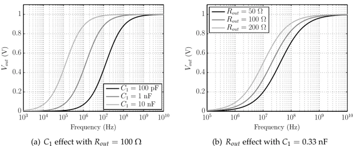
Figure 2.4(a) shows the plot of (2.10) where it can be seen the impact thatC1has on
Voutfor a given value of frequency. It is possible to see thatC1restricts the minimum value of the working frequency in order to haveVoutequal to 1 V. Figure 2.4(b) showsVoutfor
three different values ofRout. These values represent three different power output values
2.1. ANALYSIS OF THE SC DC-DC 1/2 STEP DOWN CONVERTER
CT1=10%
CT1=5%
CT1=1%
Vou
t
(V)
Frequency (Hz)
107 108 109
0.6 0.7 0.8 0.9 1 1.1
(a)CT1effect withCB1=0
CB1=10%
CB1=5%
CB1=1%
Vou
t
(V)
Frequency (Hz)
107 108 109
0.6 0.7 0.8 0.9 1 1.1
(b) CB1effect withCT1=0
Figure 2.5:Voutas function of the clock frequency forVin =2 V,C1=1 nF andRout=100Ω
Pout = 5 mW). Once again, an increase in Rout results in an increase of the minimum
working frequency in order to maintain the output voltage constant.
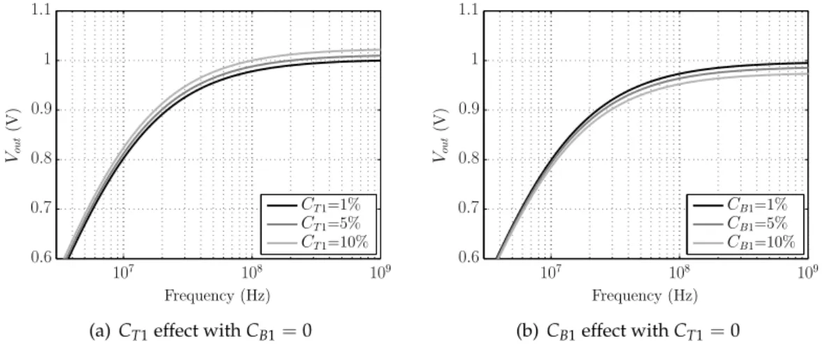
Figures 2.5(a) and 2.5(b) show the plot of (2.8) as function of the clock frequency for different values ofCT1and CB1. As CT1 increasesVout increases its value. This effect is
easily explain becauseCT1charges toVininφ1and inφ2discharges this extra voltage to
Vout. The effect ofCB1is the opposite.CB1charges toVoutinφ2, and inφ1discharge to zero. If both parasitic capacitances were equal,Voutwould remain unchanged. Nevertheless,
this extra charge and discharge will increase the current drain fromVin andVout. Even
though thatVoutremains the same, these capacitance will lead do lower efficiencies.
By solving (2.8) in order to the frequency (2.11) it is possible to determine the required frequency for the converter to produce an output voltage of 1 V (for example) for a given Vin,C1andRout.
FCLK1/2 =
Vout
Rout(2C1(Vin−2Vout) +CT1(Vin−Vout)−CB1Vout) (2.11)
considering an ideal capacitor (2.11) results in
FCLK1/2 =
Vout
2RoutC1(Vin−2Vout) (2.12)
Figure 2.6 shows the plot of (2.12) for different values of the output resistance with C1 =1 nF andVout= 1 V. ForVout =1 V the optimum point of conversion would be at
Vin =2 V. However, sinceRoutdetermines the current drain from the output node, in the
optimum point of conversion, the frequency would have to be infinite in order for the current to be larger than zero. This is why the asymptote atVin =2 V appears in the graph.
AsVin increases, the converter produces an output voltage higher than 1 V. Therefore,
in order to adjust the value ofVoutto 1 V, the amount of charge transferred toRoutmust
decrease, thus the clock frequency must decrease. WithVoutfixed at 1 V, an increase in
Routreduces the drained current - Ohms Law. Hence the amount of charge lost per time
Rout= 500 Ω Rout= 200 Ω Rout= 100 Ω
F
re
q
u
en
cy
(H
z)
Vin (V)
2 2.05 2.1 2.15 2.2 2.25 2.3 106
107 108 109
Figure 2.6: FCLKas function ofVinforVout =1 V andC1=1 nF
2.1.2 Analysis of the Efficiency
Assuming that the clock frequency is adjusted to have the desired output voltage (e.g. Vout=1 V) and that output decoupling capacitorCoutis large enough, it is reasonable to
assume that the output voltage value is constant. In this case, the schematics of the 1/2 converter circuit with an ideal output voltage supply connected toVoutduring phaseφ1 andφ2are shown in figure 2.7(a) and 2.7(b) respectively. In these,CGrepresents the gate
capacitance of all the CMOS switches in the circuit. In each clock cycle, the switches drain a charge (∆Qin2) fromVinthrough the clock buffers. Using conventional switched-capacitor
circuit analysis techniques [5](Chapter 5) it is possible to determine the charge in each capacitor at the end of each clock phase. The resulting equations are shown in (2.13) and
Vin
C1 VC1
CB1 Vout
ΔQin1 ΔQ1
CG CT1
(a) Phase 1:φ1
Vin C1
VC1
Vout
ΔQ2
CG
ΔQin2
CT1
(b) Phase 2:φ2
2.1. ANALYSIS OF THE SC DC-DC 1/2 STEP DOWN CONVERTER
these allow to determine∆Qin1,∆Qin2,∆Q1, and∆Q2.
(Vin−Vout) C1+VinCT1 =Vout (C1+CT1) +∆Q2 0=VinCG+∆Qin2
−VoutC1 = (Vout−Vin) C1+VoutCB1+∆Q1
Vout (C1+CT1) = (Vin−Vout)C1+VinCT1+∆Qin1
(2.13)
where∆Q1,2is the charge absorbed by the output power supply in each phase. Solving
the previous equations in order to∆Qin1,∆Qin2,∆Q1, and∆Q2; results in
∆Qin1 =−C1Vin−CT1Vin+2C1Vout+CT1Vout ∆Qin2 =−CGVin
∆Q1=C1Vin−2C1Vout−CB1Vout
∆Q2=C1Vin+CT1Vin−2C1Vout−CT1Vout
(2.14)
The input (Pin) and output (Pout) power are calculated using∆Qin1,∆Qin2,∆Q1,∆Q2and the values ofVin andVout. These are given by
Pin = IinVin =Vin (∆Qin1+∆Qin2) FCLK
Pout= IoutVout =Vout(∆Q1+∆Q2)FCLK
(2.15)
Pin =Vin(Vout(2C1+CT1)−Vin(C1+CG+CT1))FCLK
Pout =−Vout(−2C1Vin+4C1Vout+CB1Vout−CT1Vin+CT1Vout)FCLK
(2.16)
The efficiency (η) is defined as the ratio betweenPoutandPin, it is given by
η1/2 =
|Pout|
|Pin|
= Vout((2C1+CT1)Vin−(4C1+CB1+CT1)Vout)
Vin((C1+CG+CT1)Vin−(2C1+CT1)Vout) (2.17)
this equation can be solved forVout =1 V resulting in
η1/2 =
−Vin(2C1+CT1) +4C1+CB1+CT1
Vin(−Vin(C1+CG+CT1) +2C1+CT1) (2.18) Notice thatη1/2does not depend on the clock frequency, but only on the ratio betweenC1 and the parasitic capacitancesCT1,CB1andCG; for a given value ofVin. The 1/2 converter
circuit was simulated in Spectre with ideal switches and capacitors for different input voltages between 2 to 2.5 V and withVoutfixed at 1 V. From these transient simulations
its efficiency was calculated and compared to the efficiency calculated using (2.18) for different parasitic capacitance values.
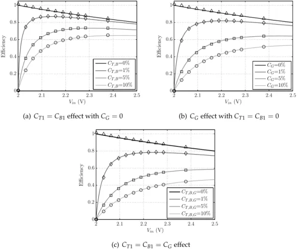
First, the effect of both top and bottom plate parasitic capacitances (CT1 =CB1) ofC1 was analysed assuming that the switch parasitic capacitancesCG = 0. Therefore, (2.18)
CB1= CT1 =0 the efficiency decreases almost in a straight line as the value ofVinincreases.
However, asCT1andCB1increases the efficiency decreases and the maximum achievable efficiency shifts to higher values ofVin. Figure 2.8(b) shows the plot of the efficiency with
the effect ofCG (CT1 = CB1 = 0). This effect is similar to the top and bottom parasitic capacitance, even though the relation between the increase ofCGand the corresponding
decrease inηis more considerable. Lastly, Fig. 2.8(c) shows the plot forCBT1 =CB1=CG.
The behaviour is similar to the previous plots, although the decrease inηis more marked. The simulation results (markers) prove that (2.18) accurately describes the behaviour of the converter efficiency and validates the theoretical analysis.
CT,B=10%
CT,B=5%
CT,B=1%
CT,B=0%
E
ffi
cie
n
cy
Vin(V)
2 2.1 2.2 2.3 2.4 2.5 0
0.2 0.4 0.6 0.8 1
(a)CT1=CB1effect withCG=0
CG=10%
CG=5%
CG=1%
CG=0%
E
ffi
cie
n
cy
Vin(V)
2 2.1 2.2 2.3 2.4 2.5 0
0.2 0.4 0.6 0.8 1
(b) CGeffect withCT1=CB1=0
CT,B,G=10%
CT,B,G=5%
CT,B,G=1%
CT,B,G=0%
E
ffi
cie
n
cy
Vin(V)
2 2.1 2.2 2.3 2.4 2.5 0
0.2 0.4 0.6 0.8 1
(c)CT1=CB1=CGeffect
Figure 2.8: Efficiency of the 1/2 converter circuit as function ofVinwithC1=1 nF,Vout=1
2.2. ANALYSIS OF THE SC DC-DC 2/3 STEP DOWN CONVERTER
2.2
Analysis of the SC DC-DC 2/3 Step Down Converter
2.2.1 Analyses of the Output Voltage
Vin
φ1
C1
Cout
Vout
φ1
φ2
Rout
φ1
C2
C3
φ1
φ2
φ2
φ2
Figure 2.9: Simplified schematic of the 2/3 SC converter
Figure 2.9 shows the topology chosen to down-convert the input voltage (Vin) into two
thirds smaller,Vout =2/3Vin [4]. The operation of this circuit is divided in two different
phases: phase one (φ1) in which the capacitorC1charges to the input voltageVin in series
with the parallel ofC2andC3; and phase two (φ2) where the capacitorC1and the series of
C2andC3are discharge.
Vin C1 Cout Rout
C2 C3
V1
V2 V3
Vout
CT2 CT3
CT1
CB1
(a) Phase 1:φ1
Vin
C1 Cout Rout
C2
C3
V1
V2
V3
CT1
CT2
Vout
CT3 CB2
(b) Phase 2:φ2
Figure 2.10: Simplified schematic of the 2/3 SC DC-DC converter in the two phases
Figures 2.10(a) and 2.10(b) shows the schematics of the resulting circuit in each clock phase (φ1andφ2). There are a total of five parasitic capacitances (CT1,CB1,CT2,CB2, and
conservation in two nodes: the one that connects the top plate ofC1,CT1, C2,CT2, and
Cout; and again the load resistor (Rout) in parallel withCout; the second node connects the
bottom plate ofC2and the top plate ofC3,CB2andCT3. Fromφ2toφ1there is again charge conservation in two nodes: the one that connects the bottom plate ofC1and the top plates ofC2,C3,CT2,CT3andCB2; the other connects the top plate ofCoutwithRout. The same
conditions in order to maintain valid (2.1) are kept in this converter.
Applying the same analyses as in the previous section, the equations that describe the conservation of charge can be seen in (2.19).
Qφ1
C1+Q φ1
CT1+Q φ1
C2+Q φ1
CT2+Q φ1
Cout =Q
φ2
C1+Q φ2
CT1+Q φ2
C2+Q φ2
CT2+Q φ2
Cout+∆QRout
−Qφ1
C2+Q φ1
C3+Q φ1
CT3 =−Q φ2
C2+Q φ2
CB2+Q φ2
C3+Q φ2
CT3 −Qφ2
C1+Q φ2
C2+Q φ2
CT2+Q φ2
C3+Q φ2
CT3 =−Q φ1
C1+Q φ1
CB1+Q φ1
C2+Q φ1
CT2+Q φ1
C3+Q φ1
CT3
Qφ2
Cout =Q
φ1
Cout+∆QRout
(2.19)
ReplacingQ=V·Cin (2.19) results in the set of equations shown below.
(Vin−V2)C1+V2(C2+CT2) +VinCT1+Vout[n−1]Cout=
=
Vout
n−1
2
−V3
C2+Vout
n−1
2 C1+Cout+CT1+CT2+
T
2Rout
V2(C3+CT3)−V2C2=
=
V3−Vout
n−1
2
C2+V3(C3+CB2+CT3)
−Vout
n−1
2
C1+
Vout
n−1
2
−V3
C2+V3(C3+CT3) +Vout
n−1
2
(CT1+CT2) =
= (V2−Vin)C1+V2(C2+C3+CB1+CT2+CT3)
Vout
n−1
2
Cout=Vout[n]
Cout+ T
2Rout
(2.20)
As in the preview section, (2.20) is solved in order toVout, then considering only the
steady state(Vout[n] = Vout[n−1] = Vout)and, finally, considering the approximation
Cout →∞. Due to the large size of the resulting equation, only the equations without the
effect of parasitics capacitances (CT1 = CB1 = CT2 = CB2 = CT3 = 0) and considering
C1 =C2 =C3in order ofTCLKorFCLKare showed (2.21) and (2.22).
Vout= 2C1RoutVin
3C1Rout+2T (2.21)
Vout= 2C1F RoutVin
3C1F Rout+2 (2.22)
Figure 2.11(a) shows the plot of (2.22) where it can be seen the impact thatC1has on
2.2. ANALYSIS OF THE SC DC-DC 2/3 STEP DOWN CONVERTER
showsVoutfor three different values of Rout. These values represent three different power
output values (Rout = 50 Ω → Pout = 20 mW, Rout = 100 Ω → Pout = 10 mW, and
Rout=200Ω→ Pout =5 mW). Once again, an increase inRoutresults in a increase of the
minimum working frequency in order to maintain the output voltage constant.
C1= 10nF
C1= 1nF
C1= 100pF
Vou
t
(V)
Frequency (Hz)
103 104 105 106 107 108 109 1010 0
0.2 0.4 0.6 0.8 1
(a)C1effect withRout=100Ω
Rout= 200 Ω Rout= 100 Ω Rout= 50 Ω
Vou
t
(V)
Frequency (Hz)
105 106 107 108 109 1010 0
0.2 0.4 0.6 0.8 1
(b) Routeffect withC1=0.33 nF Figure 2.11:Voutas function of the clock frequency forVin =1.5 V
Figures 2.12 show the plot ofVout as function of the clock frequency forVin = 2 V,
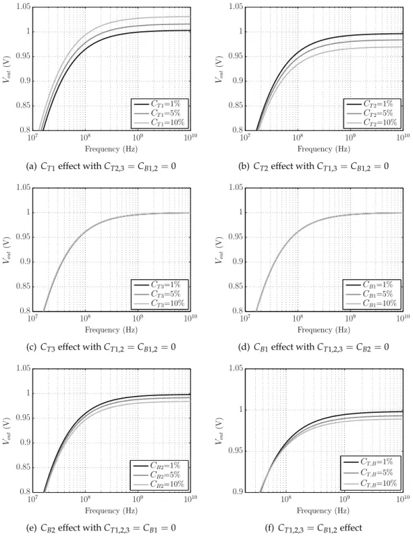
C1 =C2 =C3 =0.33 nF andRout = 100Ωfor different values ofCT1,CB1,CT2,CB2and
CT3. Figures 2.12(c) and 2.12(d) show thatCT3 andCB1have no effect inVout. The first,
CT3, charges in parallel withC3and so does not affectVout; the second,CB1, charges to
V2inφ1and inφ2 discharges to ground. Figure 2.12(a) shows that asCT1 increasesVout
increases its value. This is becauseCT1charges toVininφ1which is at a higher potential thanVoutinφ2. Figures 2.12(b) and 2.12(e) show that asCT2orCB2increaseVoutdecreases.
The first,CT2, charges toV2inφ1which is at a lower potential thanVoutinφ2, and so drain charge fromVout; the second,CB2drains charge fromV3inφ2and discharges to ground in
φ2and thefores affects theVoutvalue. Finally, Fig. 2.12(f), shows the effect if all parasitic
capacitances were equal. This results in a decrease inVout, although the decrease is very
small, almost negligible.
From (2.22) it is possible to calculate the value ofFCLKas a function ofVin,Vout,C1, and
Rout. This results in expression (2.23).
FCLK2/3 =
2Vout
2C1RoutVin−3C1RoutVout (2.23)
Figure 2.13 shows the plot of (2.23) for different values of the output resistance with C1=C2= C3 =0.33 nF and an output voltage of 1 V. WithVout=1 V this plot shows that
the optimum point of conversion would be atVin =1.5 V. The plot shows the asymptote in
Vin =1.5 V and asVinincreases, the clock frequency decreases in order to produceVout=1
CT1=10%
CT1=5%
CT1=1%
Vou
t
(V)
Frequency (Hz)
107 108 109 1010
0.8 0.85 0.9 0.95 1 1.05
(a)CT1effect withCT2,3=CB1,2=0
CT2=10%
CT2=5%
CT2=1%
Vou
t
(V)
Frequency (Hz)
107 108 109 1010
0.8 0.85 0.9 0.95 1 1.05
(b) CT2effect withCT1,3=CB1,2=0
CT3=10%
CT3=5%
CT3=1%
Vou
t
(V)
Frequency (Hz)
107 108 109 1010
0.8 0.85 0.9 0.95 1 1.05
(c)CT3effect withCT1,2=CB1,2=0
CB1=10%
CB1=5%
CB1=1%
Vou
t
(V)
Frequency (Hz)
107 108 109 1010
0.8 0.85 0.9 0.95 1 1.05
(d)CB1effect withCT1,2,3=CB2=0
CB2=10%
CB2=5%
CB2=1%
Vou
t
(V)
Frequency (Hz)
107 108 109 1010
0.8 0.85 0.9 0.95 1 1.05
(e) CB2effect withCT1,2,3=CB1=0
CT,B=10% CT,B=5% CT,B=1% Vou t (V) Frequency (Hz)
108 109 1010
0.9 0.95 1 1.05
(f) CT1,2,3=CB1,2effect
2.2. ANALYSIS OF THE SC DC-DC 2/3 STEP DOWN CONVERTER
Rout= 500 Ω
Rout= 200 Ω
Rout= 100 Ω
F
re
q
u
en
cy
(H
z)
Vin(V)
1.5 1.6 1.7 1.8 1.9 2 2.1
107 108
109
1010
Figure 2.13:FCLK2/3as function ofVinforVout =1 V andC1 =C2=C3=0.33 nF
2.2.2 Analysis of the Efficiency
The efficiency analyses, performed on the 1/2 converter, can be replicated for this converter as well. The schematics of the 2/3 converter circuit during phaseφ1 andφ2 are shown in figure 2.14(a) and 2.14(b) respectively. Using conventional switched-capacitor circuit analysis techniques [7](Chapter 5) it is possible to determine the charge in each capacitor at the end of each clock phase. The resulting equations are shown in (2.24) and these allow to determine∆Qin1,∆Qin2, and∆Qout. Where∆Qoutis the charge absorbed by the output
power supply inφ2.
CG Vin C1
C2 C3
V1
V2 V3
CT2 CT3
CT1
CB1
ΔQin1
(a) Phase 1:φ1
Vin
CG
ΔQin2
Vout
ΔQout
C1
C2
C3
V1
V2
V3
CT1
CT2
CT3 CB2
(b) Phase 2:φ2
(Vin−V2)C1+V2(C2+CT2) +VinCT1 =
=Vout(C1+CT1+CT2) + (Vout−V3)C2+∆Qout
0=VinCG+∆Qin2
V2(C3+CT3)−V2C2= (V3−Vout)C2+V3(C3+CB2+CT3)
−VoutC1+ (Vout−V3)C2+V3(C3+CT3) +VoutCT2 =
= (V2−Vin)C1+V2(C2+C3+CB1+CT2+CT3)
Vout(C1+CT1) = (Vin−V2)C1+VinCT1+∆Qin1
(2.24)
Solving the previous equations in order to∆Qin1,∆Qin2, and∆Qout; thenPin andPoutcan
be determined by replacing the resulting equations in 2.25. Pin = IinVin =Vin (∆Qin1+∆Qin2)FCLK
Pout= IoutVout=Vout∆QoutFCLK
(2.25)
The efficiency (η) withVout=1 can be determined by
η2/3 =
|Pout|
|Pin|
(2.26)
Due to the size of the resulting equation, only its plot is shown. Notice that η2/3 does not depend on the clock frequency, but only on the ratio between C1, C2 and C3 and the corresponding parasitic capacitances CT1, CB1, CT2, CB2, CT3 and CG; for a given
value ofVin. The 2/3 converter circuit was simulated in Spectre with ideal switches and
capacitors for different input voltages between 1.5 to 2.1 V and withVoutfixed at 1 V. From
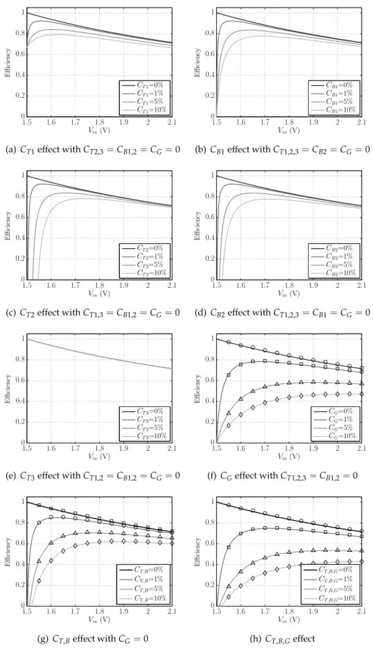
these transient simulations its efficiency was calculated and compared to the efficiency calculated using (2.26) for different parasitic capacitance values.
The previous analyses showed that the parasitic capacitances have small influence in the output voltage. However, in terms of efficiency figures 2.15 show that these have a strong impact in the efficiency. Figures 2.15(a), 2.15(b), 2.15(c) and 2.15(d) affect the efficiency almost in the same way - an increase in the capacitances result in a decrease in the efficiency. Figure 2.15(e) shows thatCT3has no impact. This is because this parasitic capacitance charge and discharge in parallel withC3and so no charge is lost. Figure 2.15(f) shows the effect ofCGwhere the decrease in the efficiency is more pronounced than one
caused if all parasitic capacitances of the flying capacitors were equal (Fig. 2.15(g)). Lastly, figure 2.15(h) shows the plot forCT,B =CG. The behaviour is the same as in the previous
2.2. ANALYSIS OF THE SC DC-DC 2/3 STEP DOWN CONVERTER
CT1=10% CT1=5% CT1=1% CT1=0%
E
ffi
cie
n
cy
Vin(V)
1.5 1.6 1.7 1.8 1.9 2 2.1
0 0.2 0.4 0.6 0.8 1
(a) CT1effect withCT2,3=CB1,2=CG=0
CB1=10% CB1=5% CB1=1% CB1=0%
E
ffi
cie
n
cy
Vin(V)
1.5 1.6 1.7 1.8 1.9 2 2.1
0 0.2 0.4 0.6 0.8 1
(b) CB1effect withCT1,2,3=CB2=CG=0
CT2=10% CT2=5% CT2=1% CT2=0%
E
ffi
cie
n
cy
Vin(V)
1.5 1.6 1.7 1.8 1.9 2 2.1
0 0.2 0.4 0.6 0.8 1
(c)CT2effect withCT1,3=CB1,2=CG=0
CB2=10% CB2=5% CB2=1% CB2=0%
E
ffi
cie
n
cy
Vin(V)
1.5 1.6 1.7 1.8 1.9 2 2.1
0 0.2 0.4 0.6 0.8 1
(d) CB2effect withCT1,2,3=CB1=CG=0
CT3=10% CT3=5% CT3=1% CT3=0%
E
ffi
cie
n
cy
Vin(V)
1.5 1.6 1.7 1.8 1.9 2 2.1
0 0.2 0.4 0.6 0.8 1
(e) CT3effect withCT1,2=CB1,2=CG=0
CG=10%
CG=5%
CG=1%
CG=0%
E
ffi
cie
n
cy
Vin(V)
1.5 1.6 1.7 1.8 1.9 2 2.1
0 0.2 0.4 0.6 0.8 1
(f) CGeffect withCT1,2,3=CB1,2=0
CT,B=10%
CT,B=5%
CT,B=1%
CT,B=0%
E
ffi
cie
n
cy
Vin(V)
1.5 1.6 1.7 1.8 1.9 2 2.1
0 0.2 0.4 0.6 0.8 1
(g) CT,Beffect withCG=0
CT,B,G=10%
CT,B,G=5%
CT,B,G=1%
CT,B,G=0%
E
ffi
cie
n
cy
Vin(V)
1.5 1.6 1.7 1.8 1.9 2 2.1
0 0.2 0.4 0.6 0.8 1
(h)CT,B,Geffect
2.3
Analysis of the SC DC-DC 1/1 Converter
2.3.1 Analyses of the Output Voltage
Vin C1 Cout
Vout
φ2
Rout
φ1
CT1
Figure 2.16: Simplified schematic of the 1/1 SC DC-DC converter
Unlike the two previous converters, this converter, show in figure 2.16, does not step-down or step-up the input voltage. Its function is simpler - transfer the input voltage (Vin)
into to the output voltage,Vout=Vin [4]. In phase one (φ1) the capacitorC1charges to the input voltage (Vin) and in phase two (φ2) the capacitorC1discharge toVout.
Vin CT1 C1 V1 Cout Rout Vout
(a) Phase 1:φ1
Vin CT1 C1 V1 Cout Rout Vout
(b) Phase 2:φ2
Figure 2.17: Simplified schematic of the 1/1 SC DC-DC converter in the two phases
Figures 2.17(a) and 2.17(b) shows the schematics of the resulting circuit in each clock phase (φ1andφ2). There is only one parasitic capacitance to have into account -CT1. From
φ1toφ2there is charge conservation in the node that connectsC1,CT1, andCouttop plates
and the load resistor (Rout). Fromφ2toφ1there is charge conservation in the node that connects Cout top plate and Rout. As in the previous converters, the assumptions that
validate the use of (2.1) are kept. Applying the same analyse as in the previous sections, the resulting system of charge equations can be seen in (2.27).
Qφ1
C1 +Q φ1
CT1+Q φ1
Cout =Q
φ2
C1+Q φ2
CT1 +Q φ2
Cout+∆QRout
Qφ2
Cout = Q
φ1
Cout+∆QRout
2.3. ANALYSIS OF THE SC DC-DC 1/1 CONVERTER
ReplacingQ=V·Cin (2.27) results in the set of equations shown below.
Vin(C1+CT1) +Vout[n−1]Cout=Vout
n− 1
2 C1+CT1+Cout+ T 2Rout
Vout
n− 1
2
Cout=Vout[n]
Cout+ T
2Rout
(2.28)
As in the previous sections, solving (2.28) in order toVout, then considering only the steady
state(Vout[n] =Vout[n−1] =Vout)and, finally, considering the approximationCout→∞;
results in
Vout= RoutVin(C1+CT1)
C1Rout+CT1Rout+T (2.29)
or as a function of the clock frequency (F=1/T)
Vout= F RoutVin(C1+CT1)
F Rout(C1+CT1) +1 (2.30) For simplicity it is possible to calculateVoutconsidering the ideal capacitor (CT1 =0) in order ofTorF.
Vout= C1RoutVin
C1Rout+T (2.31)
Vout= C1F RoutVin
C1F Rout+1 (2.32)
C1= 10nF
C1= 1nF
C1= 100pF
Vou
t
(V)
Frequency (Hz)
104 105 106 107 108 109 1010 0
0.2 0.4 0.6 0.8 1
(a)C1effect withRout=100Ω
Rout= 200 Ω Rout= 100 Ω Rout= 50 Ω
Vou
t
(V)
Frequency (Hz)
105 106 107 108 109 1010 0
0.2 0.4 0.6 0.8 1
(b) Routeffect withC1=1 nF Figure 2.18:Voutas function of the clock frequency forVin =1 V
Figure 2.18(a) shows the plot of (2.32) where it can be seen the impact thatC1has on
Voutfor a given value of frequency. As in the previous converter, the value ofC1restricts the minimum value of the working frequency in order to haveVoutequal to 1 V. Figure 2.18(b)
showsVoutfor three different values of Rout. These values represent three different power
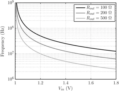
output values (Rout = 50 Ω → Pout = 20 mW, Rout = 100 Ω → Pout = 10 mW, and
Rout=200Ω→Pout =5 mW). Once again, an increase inRoutresults in an increase on