José Alberto Martins de Carvalho
Transimpedance Amplifier for Integrated
SpO2 Optic Sensor
Dissertação para obtenção do Grau de Mestre em Engenharia Electrotécnica e de Computadores
Orientador : Luís Augusto Bica Gomes de Oliveira, Prof. Auxiliar, Universidade Nova de Lisboa
Co-orientador : João Carlos da Palma Goes, Prof. Associado, Universidade Nova de Lisboa
Júri:
Presidente: Prof. Doutor Nuno Filipe Silva Veríssimo Paulino
Arguente: Prof. Doutor João Pedro Abreu de Oliveira
Vogal: Prof. Doutora Maria Manuela de Almeida Carvalho Vieira
Transimpedance Amplifier for Integrated SpO2 Optic Sensor
Copyright cJosé Alberto Martins de Carvalho, Faculdade de Ciências e Tecnologia, Uni-versidade Nova de Lisboa
UNIVERSIDADE NOVA DE LISBOA
Resumo
Faculdade de Ciências e Tecnologia
Departamento de Engenharia Electrotécnica e de Computadores
Mestre em Engenharia Electrotécnica e de Computadores
por José Alberto Martins de Carvalho
O nível de oxigenação do sangue, ou SpO2 (saturação de hemoglobina arterial como é me-dida pelo oxímetro de pulso) é um sinal vital essencial para o diagnostico médico e a sua medição por métodos não invasivos é uma das grandes inovações da medicina moderna. Esta medição pode ser efectuada pelo processamento da luz vermelha e infravermelha reflectida no dedo do paciente e recebida num fotorreceptor. Antes deste sinal ser apli-cado a um conversor analógico-digital (ADC), a corrente gerada no fotorreceptor tem de ser convertida para um sinal em tensão, e a sua amplitude ajustada por forma a usar totalmente a gama dinâmica do ADC. Uma vez que o fotorreceptor gera um sinal em cor-rente de amplitude variável, é necessário um amplificador de transimpedância (TIA) de ganho controlável. O TIA de dois andares proposto nesta tese utiliza um andar de porta comum com regulação (RCG) no primeiro andar, ao mesmo tempo que utiliza técnicas de cancelamento de ruído e de conversão de sinal single-end para diferencial, com recurso a um andar fonte comum adicional. Um segundo andar de ganho regulável é implemen-tado, baseado no amplificador MOS paramétrico (MPA), idealmente sem ruído. O MPA é um amplificador em tempo discreto, eliminando portanto a necessidade de um circuito de amostragem (S & H), na entrada do ADC. O circuito proposto foi dimensionado em tecnologia CMOS standard de 130 nm com 1.2 V de tensão de alimentação e o consumo total do circuito é inferior a 350 µW.
UNIVERSIDADE NOVA DE LISBOA
Abstract
Faculdade de Ciências e Tecnologia
Departamento de Engenharia Electrotécnica e de Computadores
Mestre em Engenharia Electrotécnica e de Computadores
por José Alberto Martins de Carvalho
Contents
Resumo 3
Abstract 5
List of Figures 9
Abbreviations 11
1 Introduction 13
1.1 Background and Motivation . . . 13
1.2 Thesis Organization . . . 14
1.3 Contributions . . . 15
2 State of the art 17 2.1 Principles of Pulse Oximetry . . . 17
2.2 Pulse Oxymeters . . . 19
2.3 Proposed Pulse Oximeter Architecture . . . 20
2.3.1 Integrated Photodiode . . . 21
2.3.2 Transimpedance Amplifiers . . . 22
2.3.3 Discrete Time Parametric Amplifier . . . 22
2.4 Noise . . . 23
2.4.1 Thermal Noise . . . 23
2.4.2 Flicker Noise . . . 24
2.5 Transimpedance Amplifier Topologies . . . 25
2.5.1 Feedback Transimpedance Amplifier . . . 25
2.5.2 Common-gate Trasimpedance amplifier . . . 28
2.5.3 Regulated Common Gate Transimpedance Amplifier . . . 30
3 Regulated Common Gate Stage 33 3.1 Working Principle . . . 34
3.2 Frequency Response of the RCG . . . 35
3.2.1 Input Impedance . . . 36
3.2.2 Transfer Function . . . 37
3.2.3 Considerations about stability . . . 37
3.3 Noise . . . 38
3.3.1 Thermal Noise . . . 38
3.3.1.1 IB1 current source . . . 39
3.3.1.2 Regulaton transistor andIB2 current source . . . 39
3.3.1.3 Input transistor . . . 40
4 Balun operation and noise cancellation techniques 43 4.1 Common-Source Stage . . . 44
4.2 LNA’s . . . 45
4.2.1 Balun Operation . . . 45
4.2.2 Noise Cancellation . . . 46
4.2.3 Distortion Cancelling . . . 47
4.2.4 Design Considerations . . . 47
4.3 TIA’s . . . 47
4.3.1 Balun Operation . . . 48
4.3.2 Noise Cancelling . . . 48
4.4 Regulated Common-Gate Stage with Noise Cancelling . . . 48
4.4.1 Balun Operation . . . 49
4.4.2 Noise Cancelling . . . 50
5 Discrete Time Parametric Amplifier with Adjustable Gain 51 5.1 Basic Principles of the DT MPA . . . 51
5.2 The MOSCAP and the three terminal MOS varactor . . . 53
5.3 The DT MPA . . . 55
5.4 Proposed DT MPA . . . 57
6 Circuit Implementation 59 6.1 Balun RCG TIA . . . 59
6.2 TIA and DTPA . . . 62
7 Conclusions and Future Work 63 7.1 Conclusions . . . 63
7.2 Future Work . . . 64
A Published Paper 65
List of Figures
2.1 Absorption spectra of Hb and HbO2. . . 18
2.2 Pulse oximeter system block diagram from [1]. . . 19
2.3 Pulse oximeter architecture. . . 20
2.4 Chip microphotograph of integrated photodiode and preamplifier in stan-dard CMOS [2]. . . 22
2.5 Models of thermal noise . . . 24
2.6 PSD of the total noise in a transistor (flicker noise and thermal noise) . . . 25
2.7 Shunt feedback transimpedance amplifier. . . 26
2.8 CG transimpedance amplifier stage. . . 28
2.9 CG transimpedance amplifier stage small signal model. . . 29
3.1 Regulated Common Gate Stage. . . 33
3.2 Feedback mechanism in source degeneration. . . 34
3.3 (a) Common Gate stage with local feedback and (b) it’s small signal equiv-alent. . . 35
3.4 RCG stage small signal equivalent circuit. . . 36
3.5 RCG stage with noise sources. . . 38
3.6 Small signal equivalent with IB2 and M2 noise source. . . 39
3.7 Small signal equivalent with M1 noise source. . . 40
4.1 Basic CG-CS topology exploiting the input transistor thermal noise can-celling. . . 43
4.2 Common-source amplifier topology. . . 44
4.3 Balun RCG exploiting thermal noise cancelling. . . 49
5.1 Principle of operation of the discrete time MOS parametric amplifier. . . . 52
5.2 Simplified cross section of a MOS Capacitor showing a simple equivalent circuit. . . 53
5.3 Typical capacitance/voltage characteristic of a NMOS capacitor. . . 54
5.4 Simulated Capacitance/voltage characteristic of a PMOS 3 terminal varactor. 55 5.5 DT MPA cell based on [3]. . . 56
5.6 Proposed DT MPA circuit. . . 57
5.7 DT MPA simulation withVgs = 0.3V,Vin = 20mV,fin = 10kHz,Fs = 100 kHz. . . 58
5.8 Hamming window FFT with 1024 points for DT MPA with Vgs = 0.3 V, fin = 10 kHz , Fs = 100kHz. . . 58
6.1 Balun RCG exploiting thermal noise cancelling. . . 59
6.2 Frequency response of the RCG (circles) and CS (triangles). . . 60
6.3 Simulated input referred noise. . . 61
Abbreviations
AC Alternating Current
ADC Analog to DigitalConverter
CG Common Gate
CMOS Complementary Metal-OxideSemiconductor
CS Common Source
DC Direct Current
DTPA Discrete Time Parametric Amplifier
IC Integrated Circuits
IR InfraRed
KCL Kirchhoff’s Current Law
LED LightEmittingDiode
LNA Low Noise Amplifier
MOSFET Metal Oxide Semiconductor Field Effect Transistor
NEF Noise ExcessFactor
PCB Printed Circuit Board
PSD Power Spectral Density
RCG Regulated Common Gate
RGC ReGulated Cascode
RF Radio Frequency
S&H Sample and Hold
SoC System on Chip
TIA TransImpedance Amplifier
VCCS Voltage Controlled Current Source
Chapter 1
Introduction
1.1
Background and Motivation
Nowadays, with the increased population demand, there is a need for better and more economic health care. It’s in this context that the need for economical and reliable devices to continuously and remotely monitor the health of a patient arises, in order for actions to be taken as soon as a change in a patients status is observed, and thus, improving the health care quality and saving costs, on the long run, by dealing with illnesses and critical conditions on it’s early stages. In modern medicine the blood oxygen level is considered to be one of the important vital signs (alongside blood pressure, heart rate, breathing rate and body temperature) and its constant monitoring can give early insight on problems in the circulatory and respiratory system.
Pulse oximeters are a non-invasive method to measure the percentage of oxygenated hemoglobin in a patients blood, and as such are ubiquitous in modern medicine, as such pulse oximeters are widely used in intensive care, operating rooms, emergency care, birth and delivery, neonatal and pediatric care, sleep studies, among others.
In traditional pulse oxymeters the transducer is usually clipped or taped to a translucent area of the patient, such as an earlobe or a finger, and wires extend from the transducer to the central processing unit, making this system not very practical for portable and wearable applications and limiting it’s usefulness.
Besides the traditional applications, there is a growing demand for a new type of devices, which focus on the remote monitoring of the patients, and so the need for novel archi-tectures built around cheap and portable solutions arises. This new devices will make possible applications, such as, home care monitoring for the elderly or chronically ill, wireless medical sensing, remote monitoring of the health status of military personnel in the battlefield as well as fire-fighters engaging in fire control, and rescue missions. It’s in this context that reducing size and power consumption is critical. Power consumption is directly related to price and size, because it directly influences battery life. More compact approaches comprising the whole transducer and analog front-end could potentially lead to cheaper and easier to use disposable systems, boosting even further the applications of this systems.
In this work a CMOS differential transimpedance amplifier (TIA) with adjustable gain that also doubles as a sample and hold (S&H) is proposed in order to be implemented in the same die as a photo-detector and ADC (Analog-To-Digital Converter) in order to build a full SoC pulse oximeter analog front end. To accommodate for different photo-sensor’s, variations in light sources and transducer positioning a controllable gain is desirable. The goal is to design a TIA that is both low power, and has a high dynamic range with controllable gain.
1.2
Thesis Organization
This thesis has been organized in six chapters, including this introductory chapter.
Chapter 2 consists of a brief overview of the pulse oximetry principles. This includes a brief explanation of the phisical aspects of the pulse oximetri measurment as well as a breif explanation of the basic blocks in the architecture. A basic overview of noise in CMOS circuits is then presented, as well as an introduction to two of the most common TIA topologies, and the principles of parametric amplification.
Chapter 1. Introduction 15
Chapter 4 presents a noise cancelling and balun operation principle. First, the known equations for the LNA CG/CS circuit are shown, and then a parallelism between the LNA and the TIA is demonstrated, and equations to guarantee simultaneous noise cancelling and balun operation are presented. From the analysis of the RCG, the proposed RCG/CS circuit is then presented with the matching conditions to assure noise cancelling and balun operation.
Chapter 5 is dedicated to the DTPA, which is the second stage of the proposed archi-tecture. First a brief analysis of the working principle of the DTPA is made. The MOS varactor that constitutes the heart of the DTPA is then presented, as well as a technique that enables the gain to be varied. The proposed DTPA is then presented with simulation results the corroborate the proposed variable gain aspect of the circuit.
Chapter 6 starts with implementation considerations for the proposed circuit. Simulation results are provided for the TIA and the complete architecture. It’s shown that the TIA has a good performance compared to other circuits with similar purposes in the literature. The DPTA is shown to work as expected in simultaneous with the TIA.
Chapter 7 comprises the overall conclusions on the work developed, as well as suggestions for further research work.
1.3
Contributions
The main contributions of this thesis are:
A novel integrated architecture for a front end amplifier for application in SpO2 sensors
is presented. The presented architecture aims at being booth low power, and low noise. The architecture comprises two main blocks, namely a transimpedance amplifier and a discrete time parametric amplifier with gain control.
A new topology is proposed for the transimpedance amplifier based on the regulated com-mon gate, and the well known comcom-mon-gate/comcom-mon-source topologies. The proposed circuit exploits booth thermal and flicker noise cancelling, while offering balun operation.
Chapter 2
State of the art
In the following sections, the physics behind the working principles of a pulse oximeter are presented in order to give a better insight on the challenges of the its design. Then the proposed pulse oximeter architecture is presented, as well as its constituting blocks.
2.1
Principles of Pulse Oximetry
The percentage of oxygen in blood as measured by the pulse oximeter(SpO2)is given by
the ratio between oxygenated hemoglobin and the total hemoglobin, as given by 2.1, where HbO2 is refers to the oxygenated hemoblogin, and Hb refers to hemoglobin with reduced
oxygen.
SpO2 =
HbO2
Hb+HbO2
(2.1)
Oxygenated hemoblogin(HbO2), which is bright red absorbs more IR light, and let’s more
red light pass through it than its de-oxygenated counter part, the dark red hemoglobin(Hb), as can be observed in Fig.2.1. It’s this different absorption characteristics for red light (660 nm) and infra-red light (940 nm) that make possible to measure the blood oxygenation by measuring the ratio of absorption of red and IR light.
The light sources, usually light-emitting diodes (LED’s) shine red and IR light through a translucent part of patients body such as an earlobe or a finger or toe. The light passes through the patients tissue, and is then measured with a photo-sensor, usually a
Figure 2.1: Absorption spectra ofHb andHbO2.
photo-diode. Light has to travel through other tissues, such as skin, bones and muscle, but fortunately blood vessels expand and contract with the heart beat so the oximeter signal appears modulated, making it possible to effectively separate the blood transmission characteristics, an AC signal, from the transmission characteristics of the unmodulated tissue in the background, a DC signal.
The physics behind the working principle of the pulse oximeter are based on the Beer-Lambert law. Beer’s law relates the transmitted and incident light through a medium that contains an absorving substance of concentration C and lenght l acording to 2.2, where IT RAN S and IIN C are the intensity of the transmitted and incident light respectively.
IT RAN S(t) =IIN Ce−ε(λ)CL (2.2)
We can define the transmittanceT asIT RAN S/IIN C and the absorbanceAas−ln(T), and
we obtain the total light absorbance of blood that is given by
Abld(t) = [εHbO2(λR)CHbO2+εHb(λR)CHb]L (2.3)
We have stated before that the blood vessels expand and contract, so it can be established that their thickness varies, and so does the observance of the blood in them withLin 2.3. If we define R to be the ratio of relative absorbances at the red and IR wavelenghts we get,
R = ln(iH,R/iL,R) ln(iH,R/iL,R) ≈
iR ac/iRDC
iIR ac/IDCIR = εHbO2(λR)CHbO2+εHb(λR)CHb
εHbO2(λIR)CHbO2+εHb(λIR)CHb
Chapter 2. State of the art 19
It’s known that the right-hand side of equation 2.4 is a good aproximation of the left-hand side, considering that the ac signals are very small when compared to the dc component. Whe can then combinine equations 2.1 and 2.4 to obtain
SpO2 =
εHb(λR)−εHb(λIR)R
εHb(λR)−εHbO2(λR) + [εHbO2λ(IR)−εHb(λIR)]R
×100% (2.5)
The absorbances for Hb and HbO2 are know for the red and IR wavelenghts, so it’s now
clear that the value that the pulse oxymeter measures is the ratioR, wich relates to SpO2
by means of equation 2.5.
2.2
Pulse Oxymeters
Pulse oxymeters usually are comprised of two parts, a sensing probe, and a control unit. Usually the sensing probe consists of the transducer and the light sources, while the control unit takes care of the signal conditioning, data acquisition, signal processing and data display. A typical system level architecture is depicted in Fig. 2.2[1].
Figure 2.2: Pulse oximeter system block diagram from [1].
digital processing clears the signal, and computes the SpO2 by computing the ratios of
absorbance acording to the principles explained in the previous section. Note that most of the power consumption can be traced back to the the user interface and signal processing.
One big inconvenience of this type of traditional systems is that the sensing probe has to be connected via a wire to the main unit. Albeit being perfectly useful in a situation where a patient is in a hospital bed, for applications such as home care monitoring for the elderly or chronically ill, wireless medical sensing, remote monitoring of the health status of military personnel in the battlefield as well as fire-fighters engaging in fire control, and rescue missions among others, proves to be a severe constraint.
2.3
Proposed Pulse Oximeter Architecture
In contrast to the traditional pulse oxymeter architectures, the proposed work is based on an architecture where the photodetector and analog front end are separated from the data display and signal processing. This way, we can have a low power probe, that uses a small battery attached to the patient, while a device such as a smart phone is connected wirelessly to the probe and handles the power consuming signal processing and data display. The architecture for the proposed pulse oxymeter front-end is depicted on Fig. 2.3. By decoupling the analog front end from the rest of the circuit, a low power solution can be obtained, while it’s expected that by integrating the photodetector with the analog front end might lead to reduced cost’s, and greater usability. This comes from the fact that no wires are needed for the sensor itself.
Human Tissue
TIA
DTPA
ΣΔVCtrl
ϕ1 ϕ2
Figure 2.3: Pulse oximeter architecture.
Chapter 2. State of the art 21
the ADC, and once the signal is in the digital domain it can finally be sent wirelessly to a remote device for signal processing. This device can be a bluetooth capable smart phone, that can easily log the patients status for a long time. By using this architecture, several other sensors can be used to create wearable integrated remote monitoring device for medical applications by using time division multiplexing in order for the ADC and wireless module to be shared with the rest of the sensors.
2.3.1
Integrated Photodiode
In order to convert light signal into an electrical signal some sort of transducer must be used. The photodiode is a type of photodetector that converts a light signal into a current signal. Like a normal diode a photodiode consists of a p-n junction. When a photon of sufficient energy is absorbed in the photodiodes p and n regions an electron-hole pair is generated. Although in the bulk region these electron electron-hole pairs have a high chance of recombining, in the depletion region and a a diffusion width on either side of it, the existing electric field quickly sweeps the electrons to the n side and the holes to the p side. This creates a photocurrent, which is proportional to the incident light. Any p-n junction is a potential photodiode, this is the reason why devices containing p-n junctions are encapsulated in opaque packages in order to prevent any photocurrent induced malfunctions. With careful design, one can implement a photodiode in the same die as the rest of the circuit, resulting in a more compact and cheaper monolithic approach. In the past several work has been done in the area of integrated photodiodes in standard CMOS technologies, namely for CMOS image sensors [5], optic communications [2], and others. One example of an integrated photodiode can be seen in Fig. 2.4 [2], where a photiode for optical comunications is integrated in the same die as the TIA.
Figure 2.4: Chip microphotograph of integrated photodiode and preamplifier in
stan-dard CMOS [2].
2.3.2
Transimpedance Amplifiers
Traditionally amplifiers sense voltages at their input and amplify them in their output. Other types of amplifiers also exist, namely amplifiers that sense currents and output voltages. This "current-voltage" amplifiers are effectively a current controlled voltage source (CCVS) and are commonly know as transimpedance (TIA) amplifiers. Ideally the input impedance should be zero much like an ideal current meter. Likewise the output impedance should also be zero as in a ideal voltage source. The transimpedance gain is then defined as Ro =vout/iin.
2.3.3
Discrete Time Parametric Amplifier
Parametric amplifiers work by the change of a parameter within the amplifier. In this particular case, amplification is made through the variation of a sampling capacitor. This can be simply described by taking the equation for the charge in a capacitor, given by Q =C·V. If we can vary the capacitance from an initial value C1, to a lower value C2
while conserving the charge in the capacitor we can obtain a gain expressed as:
Av =
Vo
Vin = C1
C2
(2.6)
Chapter 2. State of the art 23
initial or final capacitance could be varied, one could obtain a variable gain. In the proposed circuit presented in the next chapters this possibility is pursued further.
2.4
Noise
In electronic circuits, we consider noise to be a random unwanted signals. This signals are generated in electronic devices due to different physical phenomena. Noise in electronic circuits comes from the fact that charge is carried in discrete amounts equal to an electrons charge [10][11]. These small fluctuations of charge create small fluctuations in the current and voltage at the macroscopic level that are perceived as noise. Although the presence of noise in electronic circuits can be desired and useful, such as in some oscillators, usually noise limits the circuits performance. When dealing with low power signals, it’s crucial that the noise is not of the same order of magnitude as the signal itself, otherwise that would make the two signals indistinct. Noise also limits the upper limit of an amplifiers gain to Vdd/vn where Vdd is the supply voltage and vn is the noise floor at the input of
the amplifier [11]. A gain larger thenVdd/vnwould simply saturate the transistor, leaving
no output dynamic range for the input signal. Although noise is by definition a random signal in the time domain, its average power and frequency spectrum can be quantified. In this section two of the most common noise sources in CMOS transistors are described.
2.4.1
Thermal Noise
In every conductor at a temperature different then 0 K there is a random motion of electrons. This random motion creates what is usually referred to as thermal noise. In a resistor the noise generated by thermal noise can be expressed as [12][10]
v2
nRes = 4kT R∆f (2.7)
Vn2
R
*
(a)
M1 In2
(b)
Figure 2.5: Models of the thermal noise in a resistor (a) and a MOS transistor (b).
The same phenomena that occurs in resistors, also occurs in a MOS transistor conducting channel. Usually thermal noise in a MOS transistor is modelled with a current source between drain and source as can be seen inf Fig.2.5(b) (b). It can be proved that for long channel MOS devices in the saturation region the thermal noise in the transistor channel can be expressed as [12],
v2
nM OS = 4kT gmγ∆f (2.8)
where T and k are the absolute temperature and Boltzmann constant respectively, ∆f is the bandwidth of the system, gm is the transistors transconductance and γ is the noise excess factor (NEF). For long channel devices the NEF can be derived to be equal to 2/3
but it’s higher for submicron transistors [12].
2.4.2
Flicker Noise
Another type of noise is also present in MOS transistors. Flicker noise is thought to be caused by the impurities in the interface between the gate oxide and the silicon substrate. Unlike the thermal noise flicker noise power can’t be predicted easily [12], and it’s quan-tification is still largely based on empirical considerations [11]. Flicker noise has a PSD of 1/fn withn
≈1. In Fig.2.6 the total noise power (flicker and thermal noise) of a MOS
transistor is presented. One can see that until the corner frequency fc the flicker noise is
Chapter 2. State of the art 25
fc Flicker Noise
Thermal Noise
Figure 2.6: PSD of the total noise in a transistor (flicker noise and thermal noise)
Flicker noise is modelled by a voltage source in series with the transistor gate with a power roughly given by [12]
v2
nf MOS =
K CoxW L
1
fn (2.9)
where K is a process dependent constant, Cox is the gate oxide capacitance per unity
area, andW and Lare the transistors width and length respectively. Cleaner fabrication processes result in lower values for K, and thus in lower flicker noise values. Also PMOS transistors have lowerK values then NMOS transistors, and thus have less flicker noise.
2.5
Transimpedance Amplifier Topologies
In this section, a brief analysis of three common TIA’s is presented. Simple equations for the transimpedance gain, input impedance are derived, as well as equations relating to the noise performance of the TIA’s.
2.5.1
Feedback Transimpedance Amplifier
The feedback TIA is commonly used in optoelectronic integrated circuits [13]. It consists of an operational amplifier (OA) with feedback shunt-shunt feedback topology as illustrated in Fig. 2.7.
Cf
Rf
Iin Cd
Figure 2.7: Shunt feedback transimpedance amplifier.
that the gain of the opamp is very high and frequency independent we can write
Vo
Zf
=Iin (2.10)
where Zf is the feedback impedance given by Rf//sC1f. By this means we can achieve
a high tranimpedance gain, while maintaining a very low input impedance. Considering that the OA has a dominant pole as in [14] it’s transfer function is given by equation 2.11. and it’s GBW is given by equation 2.12
A(s) = A0 1 +sτa
(2.11)
B =A0ωa=
A0
τa
(2.12)
We know that the voltage in the negative input of the op-amp is given byVo(s)/A(s)we
can write the Kirchhoff current law (KCL) to the input node thus obtaining
Vo(s)− VAo((ss))
Zf
+Iin(s)− Vo(s)
A(s)
s Cd= 0 (2.13)
Rearranging equation 2.13 and rewriting the op-amp transfer functionA(s)with equations
2.11 and 2.12 we can then obtain the transimpedance function of the feedback TIA.
Vo(s)
Iin(s)
=− Rf
s2R
fCdB−1 +sRf(Cf +ACd0) + 1
Chapter 2. State of the art 27
Since we know that the voltage at the input node is given by Vo(s)
A(s) we can derive the input
impedance.
Vo(s)
Vin(s)
=A(s)⇔ Vo(s)
Iin(s)Zin(s)
=A(s)⇔Zin =
Vo(s)
Iin(s) 1
A(s) (2.15)
Zin(s) = −
Rf
s2R
fCdB−1 +sRf(Cf +CAd0) + 1 · 1
A0
+sB−1 (2.16)
While studying the feedback TIA it’s also important to have some insight into it’s noise performance. For this study we will assume that the noise generated in the opamp can be modelled by a voltage source in series with the input of the amplifier. Note that the opamp can be designed in a way that dominant noise contribution is originated in the input transistor and that it’s contribution to the total noise can be shown to be dominant over the feedback resistors noise [14]. Thermal noise in a MOS transistor can be modelled by a current source between source and drain and flicker noise by a voltage source in series with the gate [12]. In order to simplify the analysis we can transform the thermal noise current into a equivalent voltage in series with the gate. Taking the equations for thermal and flicker noise already presented in the previous section, we get the equivalent input noise voltage of the opamp to be,
v2
na = 4kT γgm−1 +
K CoxW L ·
1
f, (2.17)
where k is the Boltzmann constant,γ is a channel length dependant coefficient, K is a process dependent constant, andCoxW L is the gate capacitance [12].
The noise transfer function for the feedback is derived in [14] and is given by
N(s) = Vno
Vna
=− 1 +sRfCd
s2R
fCdB−1+sRf(Cf +CAdo) + 1
(2.18)
Note that the complexity and area needed for a good performance opamp could lead to an increased cost.
2.5.2
Common-gate Trasimpedance amplifier
Another basic TIA topology commonly used is the common-gate (CG) stage presented in Fig. 2.8, where IB1 and VBias are a bias current and voltage, respectively. This
topol-ogy is know for it’s low input impedance and broadband [6]. Since the input current at the transistors source equals the output current at the transistors drain, ideally the transimpedance gain would be equal to Rx. Intuitively the common-gate stage acts as a
current buffer, while the I-V conversion is performed at the output by the load resistor Rx. It’s then important to know it’s input impedance.
VBias
IB1 Iin
M1
Cd
Rx VDD
VoCG
Figure 2.8: CG transimpedance amplifier stage.
By observing the small signal equivalent in Fig. 2.9 and disregarding the parasitic capac-itances, noting that the bulk and gate are tied to ground we can write
Vin =−vgs =vsb =vs (2.19)
Iin =
Vin−IoutRx
ro −
Chapter 2. State of the art 29
Iin
gm.vgs
Rx
Vo
gmb.vbs
ro
Source
Source
Drain
Gate
Cin
Co
Figure 2.9: CG transimpedance amplifier stage small signal model.
By combining equations 2.19 and 2.20 and having Zin = Vin/Iin we obtain the input
impedance for low frequencies to be given by
Zin=
ro+Rx 1 + (gm+gmb)ro
= 1 1
ro +gm+gmb
1 + Rx
ro
(2.21)
From equation 2.21 some considerations can be made. First, note that input impedance depends on the loadRx, divided byro. Sincerois usually very high, for low gain amplifiers
where Rx is relatively small we can approximate Zin = 1/(gm+gmB) as in [14]. For
high gain amplifiers and sub-micron technologies, where ro and RX can be of the same
order of magnitude this relation between gain and input impedance must be taken into account. The body effect effectively lowers the input impedance. Also note that the output impedance of the biasing current source wasn’t considered because it’s high compared with the CG input impedance, with which it’s in parallel. Since the gate and bulk are booth tied to ground, one can easily generalize equation 2.21 for high frequencies. By replacing Rx
withRx//sC1D whereCD is the total capacitance in the drain node (CD =Cdb+Cgd+CX)
and then making the parallel of this modified input impedance with 1
sCS where CS equal
to the total capacitance in the source node (CS =Cs+Cgs+Csb) we obtaining equation
2.22.
Zin(s) =
sRxroCD +Rx+ro
s2R
xroCDCS+sRx(CD +CS+ (gm+gmb)roCD) +sroCS+ (gm+gmb)ro+ 1
By combining the voltage gain and the the input impedance, the transimpedance function can be obtained. Equation 2.23 is the common-gate voltage gain Vout(s)/Vin(s) derived
from [12].
Vout(s)
Vin(s)
= Rx(ro(gm+gmb) + 1)
sRxroCD+Rx+ro
(2.23)
Since the numerator of 2.22 and denominator of 2.23 cancel out, it’s straightforward to obtain the transimpedance functionA(s)in equation 2.24. Note that as stated before, for low frequencies the tranimpedance gain equals Rx ,
A(s) = Rx(ro(gm+gmb) + 1)
s2R
xroCDCS+sRx(CD +CS+ (gm+gmb)roCD) +sroCS+ (gm+gmb)ro+ 1
. (2.24)
In the common-gate TIA there are three noise current sources relating to the thermal noise of the common-gate transistor, the noise in the drain resistor Rx and the noise of
the bias current IB. It can be shown that the noise contribution of the common-gate
transistor is dominant and has a noise transfer function given by [14]
Vno
In(s)
=− Rx
gm∗Rob
1 +sRoB (1 +sgm−1C
S)(1 +sRxCD)
(2.25)
Although from equation 2.25 the noise might appear to decrease with gm because it’s in the denominator, if we consider the total integrated output noise the effect of the reduction of the bandwith with a decrease ingm is actually dominant as proved in [14]. So in order to decrease the total output noise a lower gm is required, which conflicts with the need to have a high gm in order to obtain a low input impedance.
2.5.3
Regulated Common Gate Transimpedance Amplifier
Chapter 2. State of the art 31
name will be used trough out this work since it better reflects the working principle of this amplifier.
Chapter 3
Regulated Common Gate Stage
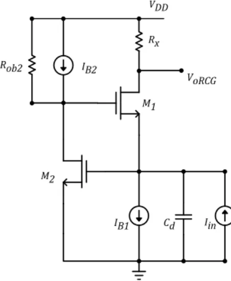
The regulated common gate (RCG) stage presented in Fig. 3.1 is a widely known TIA. It derives from the CG, in which, a gm boosting technique that consists of a local feedback loop is applied. In this Chapter, an intuitive explanation of how the RCG works is done besides a more in depth analysis of the key parameters of the RCG TIA. Transimpedance gain, input impedance and noise performance is studied. The derived equations are vali-dated by simulation.
IB2
IB1 Iin
M2
M1
Cd Rx
VoRCG VDD
Rob2
Figure 3.1: Regulated Common Gate Stage.
3.1
Working Principle
The RCG TIA, derives from the CG TIA. By applying a local feedback loop the RCG is capable of a lower input impedance then the CG stage with the same input transistor bias current and thus the same gm. This effectively increases the bandwidth by moving the input pole into higher frequencies while maintaining a good noise performance.
The effect that the source degeneration has in increasing both input and output impedance by a factor of 1 + gmRS is well known. This feedback mechanism can be intuitively
understood if ones thinks of a transistor as a transconductance amplifier as in Fig.3.2, where the output current is equal to the negative input current.
iout
RS V+
V-gm
RS V+
V-iout iout
Figure 3.2: Feedback mechanism in source degeneration.
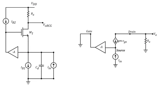
The source resistance effectively generates a series-series feedback loop by converting the output current into a voltage, while it’s applied to the negative input of the transcon-ductance amplifier. By using this principle with an active load we obtain the regular cascode circuit. This same concept can be applied to the common gate amplifier using an active feedback loop as depicted in Fig.3.3(a). This feedback loop then has the effect of decreasing the input impedance. In order to obtain negative feedback, a CS stage is used thus obtaining the circuit in Fig. 3.1.
By taking the simplified small signal equivalent in Fig.3.3(b) we can derive the approx-imate input impedance and transimpedance gain of the RCG. By observing the small signal circuit we can write
vgs =−A·vin−vin=−(A+ 1)vin (3.1)
iin =iin= (A+ 1)vingm1 (3.2)
Chapter 3. Regulated Common Gate Stage 35
IB2
IB1 Iin M1
Cd Rx
VoRCG VDD
-A
Iin
gm.vgs Rx Vo
Source Source
Drain Gate
-A
Figure 3.3: (a) Common Gate stage with local feedback and (b) it’s small signal
equivalent.
Zin =
1 (A+ 1)gm1
. (3.3)
Compared to the CG stage, the input impedance is now A times smaller. In regards to the transimpedance gain, it’s easy to see that the input current is the same as the output current. Like the CG stage the RCG effectively works as a current conveyor, where the current-voltage conversion is accomplished in the load resistor Rx.
3.2
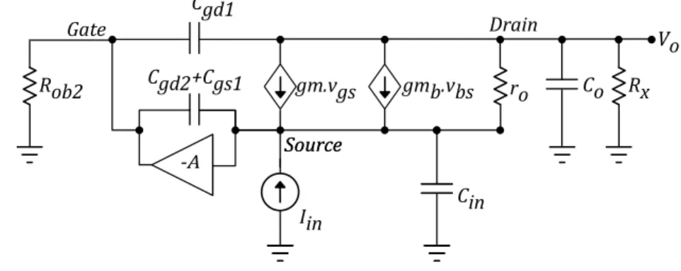
Frequency Response of the RCG
In the small signal equivalent circuit in the previous chapter, the transistors output resis-tance was discarded, as well as all the capacities present. If we take into account all the capacities involved we obtain the small circuits circuit in Fig. 3.4 whereCin is the sum of
the photodiode capacitance and the transistors parasitic capacitanceCsb, andCo is equal
to a load capacitance plusCdb.
The gain −A in the Fig. 3.4 is obtained via a CS gain stage so for low frequencies it is approximately equal to
AvCS =−gm2
ro2Rob2
ro2+Rob2
Iin gm.vgs Rx Vo gmb.vbs ro Source Source Drain Gate Cin Co -A Cgd1 Cgd2+Cgs1 Rob2
Figure 3.4: RCG stage small signal equivalent circuit.
If we look into the small signal equivalent we can write the total input capacitance by taking the miller effect into acount, and thus obtaining
C′
in =Cin+ (1 +A)(Cgs+Cgd2+Cgs1) = Cd+Csb+ (1 +A)(Cgs+Cgd2+Cgs1) (3.5)
3.2.1
Input Impedance
The impedance of the total input capacitance,C′
in, is in parallel with the input impedance
for small signals. For simplicity we will disregard the input capacitor, and then add its contribution in the end. We can then write the input current to be given by equation
Iin=−gm1Vgs−gmbVbs+ 1
ro1
(Vin−(Rx//Co)Iin) (3.6)
We can then writeVgs =−(A+ 1)Vin, so comparing to the CG stage, where Vgs =Vsb, in
the RCG Vgsis (A+ 1) times bigger then Vsb. Sincegmb is already smaller then gm, the
current caused by the body effect can be neglected. We can now write
Iin
1 + Rx
(sRxCo+ 1)ro
=Vin
(A+ 1)gm1+
1
ro
(3.7)
and from there obtain the following equation for the input impedance without considering the input capacitance
Z′
in =
Vin
Iin
= 1
(A+ 1)gm1+ r1o
+
Rx
(sRxCo+1)ro (A+ 1)gm1+ r1o
Chapter 3. Regulated Common Gate Stage 37
Now we just have to make Z′
in//sC1′
in to obtain the input impedance.
3.2.2
Transfer Function
As noted before, the input current is divided between the input impedance, and C′
in.
Noting that we are dealing with a current divider, the incremental source current in M1
can then be expressed as
Is1 =
1/sC′
in
Z′
in+ 1/sCin′
Iin =
1 1 +sZ′
inCin′
Iin (3.9)
which can be written in the form 1
1+sτ1Iin whereτ1 =Z
′
inCin′ . This current flows through
the output impedanceZx = 1+sRRxxCo. Whe can then write the approximate transimpedance
function to be given by
Vo
Id ≈
Rx (1 +sC′
in
1+ Rx
(sRxCo+1)ro
(A+1)gm1+ro1 )(1 +sRxCo)
(3.10)
3.2.3
Considerations about stability
The approximate transfer function derived before could lead one to believe that this RCG is always stable, but because it has a feedback loop, the stability of the amplifier should be studied. From the approximations made, the transfer function has two poles, at the input and output, while the loop gain only has one pole. This might lead one to believe that the system is intrinsically stable, because the maximum phase shift in a 1 pole system is
90◦, thus meeting the criteria for a stable system that the loop gain must be lower then unity when the phase has shifted by180◦. However the common-source stage used in the loop gain has two poles. This third pole can be traced back to the node at the gate of the input transistor. This pole is approximately given by
τ = (Rob2//ro2)·
(Cgd2+Cgs1)(1−A−1) +Cdb2
(3.11)
In [16] it’s suggested that this pole has to be in a frequency at least three times higher then the frequency in which the loop gain is lower then one. This should allow for a phase margin of72◦, which should guarantee there is not any overshoot in the time domain [16].
3.3
Noise
For the noise analysis we will first determine the noise voltage spectral density at the out-put. For wideband circuits the flicker noise can be neglected [14]. Since in pulse oximetry the signals involved are low frequency by nature, flicker noise should be considered. In Fig. 3.5 all the noise sources of the RCG stage are represented.
IB2
IB1 Iin
M2
M1
Cd Rx
VDD
*
*
*
InM12
InB22
InB12
InM22
VnM12
VnM22
VnRx2
Vo
Figure 3.5: RCG stage with noise sources.
3.3.1
Thermal Noise
The noise sources present in Fig. 3.5 are related to the thermal and flicker noise. We will first consider the thermal noise sources, generated by the current sourcesI2
nB1,InB2 2,InM2 2
and I2
Chapter 3. Regulated Common Gate Stage 39
3.3.1.1 IB1 current source
The noise contribution of the input transistor biasing current source is given by I2
nB1.
It can be seen in Fig. 3.5 that it is in parallel with the input current, so it’s noise transfer function,Vno/InB1 is equal to the RCG transfer function given by 3.10. The noise
contribution to the total output noise can then be expressed as
V2
nOut, B1 = InB2 1·
Rx (1 +sC′
in
1+ Rx
(sRxCo+1)ro
(A+1)gm1+ro1 )(1 +sRxCo)
2 (3.12)
3.3.1.2 Regulaton transistor and IB2 current source
In the small signal equivalent, where Vdd is short-circuited to ground, the noise currents
generated by the regulation transistor, M2, and given by InM2 2, and the noise from the
biasing current source IB2, given by InB2 2 are in parallel, so they share the same noise
transfer function. gm.vgs Rx Vo Source Source Drain Gate Cin Co -A
Rob2 // ro2 In2
Figure 3.6: Small signal equivalent with IB2 and M2 noise source.
By taking the simplified small signal circuit in Fig. 3.6 we can derive the noise transfer function. We start by writing the straightforward voltages at the gate, source and drain of the transistor thus obtaining the following equations.
Vg =−AVs+InRob2//ro2 (3.13)
Vs =gmVgs 1
sCin (3.14)
Vo =gmVgs
Rx
sRxCo
Combining equations 3.13 and 3.14 we can write In as follows
In=
VgssCin+gmVgs(A+ 1)
sCinRx
(3.16)
We can obtain the noise transfer function by dividing equations 3.15 by 3.16 thus obtaining the noise transfer function Vno/In bellow.
Vno
In
= s
Rob2//ro2RxCin
(A+1)
(s Cin
gm(A+1) + 1)(sRxCo+ 1)
(3.17)
3.3.1.3 Input transistor
We will now analyse the effect of the input transistors thermal noise. Note that in the common-gate stage, this was the dominant noise source.
gm.vgs Rx Vo Source Source Drain Gate Cin Co -A In2 Rob1 ro1
Figure 3.7: Small signal equivalent with M1 noise source.
Using the small signal circuit in Fig. 3.7 we will now derive the noise transfer function. We can write the voltage at the output node as
Vo =
Rx
sRxCo+ 1
gm1(A+ 1)Vs+
Vs−Vo
ro1
+In
(3.18)
Vo
1 + Rx
(1 +sRxCo)ro1
= Rx
1 +sRxCo ·
(In+gm1(A+ 1)Vs) (3.19)
whereVsis the voltage at the source node, and in equation 3.19 we have taken into acount
thatgm1(A+1)>> 1/ro1. Since the current at the output node is the same as the current
in the input, we can write Vs in terms of Vo so we have
Vs=Vo·
sRxCo+ 1
Rx ·
Rob1
sRob1Cin+ 1
Chapter 3. Regulated Common Gate Stage 41
Combining equations 3.19 and 3.20 with then obtain
Vo
1 + Rx
(sRxCo+ 1)ro1 −
gm1(A+ 1)
Rob1
sRob1Cin+ 1
= Rx
1 +sRxCo
In (3.21)
We know simplify the multiplying factor of Vo in the left-hand side of equation 3.21 o
obtain the the factorized equation in 3.22.
(sRxCo+ 1)(sRob1Cin+ 1) +Rx/ro1(sRob1Cin+ 1) +gm1(A+ 1)Rob1(sRxCo+ 1) (sRxCo+ 1)(sRob1Cin+ 1)
(3.22)
In order to further simplify 3.22, we will assume thatgm1(A+ 1)Rob1 >> Rx andgm(A+ 1)Cx >> Cin/ro1. With this simplifications, and equations 3.20 and 3.21 we can then
write the noise transfer function below.
Vo
In
= Rx
gm1(A+ 1)Rob1
1 +sRob1Cin (s Cin
gm1(A+1) + 1)(sRxCo)
Chapter 4
Balun operation and noise cancellation
techniques
Differential operation has many benefits, such as reducing second-order distorion and rejection of power supply and substrate noise[17] . Many RF wideband LNA circuits have been publishing integrating the LNA and balun in the same circuit, while exploiting the noise cancellation technique proposed in [18]. This consists of a CG stage in parallel with a CS stage, as depicted in Fig. 4.1.
VBias
IDC M1
Rx
VDD
Vout + +
Rx Vout
-_
M2 Rs
Rs
In1
Vin Vn,in
Vs
Vn,out2 Vn,out1
Figure 4.1: Basic CG-CS topology exploiting the input transistor thermal noise
can-celling.
The basic principle is clearly illustrated in Fig. 4.1. The input current, Iin, generates a
voltage ,Vin at the input node. This voltage is given by the product of the input current
and the input impedance. This voltage is then amplified on the CG stage, thus creating
a in phase output voltage Vout+. Since Vin is also amplified by the CS, at the CS output
we have Vout− in phase opposition to Vin and Vout+. The gain can then be expressed as
AvCS =AvCG+AvCS (4.1)
which is the sum of the gain of the CG stage and the CS stage. Assuming both the CG and CS gains are matched, by taking the output as Vout+ −Vout− we achieve our differential output, and consequently increase the gain by 6 dB. In a analogous way, the thermal noise, represented by the current source between the source and drain of the input transistor,M1, generates a noise voltageVnCG at the output node, and an anti-phase noise
voltage, VnIN. When VnIN is amplified by the CS stage, we obtain a noise voltage, VnCS,
which is in phase withVnCG. The noise cancels because it becomes a common-mode signal
at the differential output. Comparatively to other noise cancelling techniques employing feedback, this is a strictly feed-forward technique, so instability risks are greatly relaxed [18].
4.1
Common-Source Stage
Some considerations must be made in regards to the common-source stage being added to the circuit. The basic common-source topology is presented in Fig. 4.2.
Vin
M1 Rx VDD
VoutCS
Figure 4.2: Common-source amplifier topology.
Chapter 4. Balun Operation and Noise Cancelling 45
AvCS =−gm
roRx
ro+Rx ≈ −
gmRx (4.2)
Since the photodiodes input capacitance is high and we are interested in low frequencies, the CS transistor parasitic capacitances aren’t expected to degrade the bandwidth and input impedance significantly. Unfortunately, in order to obtain differential operation and noise cancelling, we are adding new noise sources which should be considered.
The flicker and thermal noise of the transistor, can be expressed as 4.3 and 4.4
v2
nf CS =
K CoxW L
1
fn ·(gmRx)
2 (4.3)
v2
ntCS = 4kT γR2x (4.4)
Note that booth of these noise sources will be added to the total output noise in order to obtain the differential gain. Since the gain is doubled, a better noise factor can be achieved in some situations. Careful design should guarantee that the benefits of adding the CS stage aren’t surpassed by the additional noise introduced.
4.2
LNA’s
As said earlier, the CG-CS topology has been reported in a multiple applications for wide-band LNA’s. We will now show some simple equations that allow both a balanced differential output and noise cancelling.
4.2.1
Balun Operation
To achieve the balun operation, it’s crucial that booth stages have the same gain. Simple equations for the conditions in which the gain is balanced can be derived. For CG stage, we know from our previous analysis that the input and output current are the same, and as such, the output voltage is given by Vo =RxIin. We can then write
Iin=Io =
Vout+
Rx
= Rx
AvCG
where AvCG is the voltage gain of the CG amplifier stage and is aproximately equal to
gm·Rx. Since the input impedance is also known to be approximately given by1/gmCG,
and for a LNA the equal the source resistance, RS we get that the gain of the CG stage
to be given by [17]
AvCG =
Rx
Zin = Rx
RS
(4.6)
Since the gain has to be balanced, but in phase opposition, the gain of the CS stage is then given by
AvCS =−
Rx
RS
(4.7)
If the condition in 4.7 is met, then the LNA will have a balanced balun operation. We shall now derive the equations that guarantee that we can also cancel the thermal noise. We will now study the conditions required to cancel the thermal noise produced by the CG input transistor, modelled by the current source In in Fig. 4.1.
4.2.2
Noise Cancellation
In the CG-CS, the thermal noise current generates a voltage at the input node, and a fully correlated anti-phase voltage at the CG output [17]. The voltage at the input can be expressed as VnIN = α1 ·In · RS while the output voltage can be written as
VnCG =−α1·In·Rx, where α1 accounts for the the voltage division between RS and Zin,
which is 1/2 when the input is matched. In order for the noise to cancel, we must have VnCG =VnCS. We can write the output noise voltage at the CS stage as 4.8 bellow.
VnCS =VnIN ·AvCS =α1·In·RS·AvCS (4.8)
Chapter 4. Balun Operation and Noise Cancelling 47
4.2.3
Distortion Cancelling
The proposed technique cancels all signals that can be modelled as a current source between the drain and source as such, in [18] it’s shown that this can effectively cancel the nonlinearity of the input transistor, assuming it’s modeled as a current source controlled by the gate. In [17] further proof is presented that all the noise and distortion currents generated by the input transistor can be cancelled. It’s also shown that the gain of the CS required for the distortion products of the CG is the same required to guarantee noise cancelling and output balancing.
4.2.4
Design Considerations
From the equations derived in the previous subsections two different design options can be considered while maintaining balanced balun operation and noise cancelling.
1) The traditional way to implement the CG-CS amplifier is with balanced gains on the CG and CS. For simplicity gmCS =gmCG and RCS =RCG
2) The transconductance of the CS stage is sized to ben times bigger than the transcon-ductance of the CG stage, while the load resistor of the CG stage is ntimes smaller. This was the design option chosen in [17] to minimize the noise contribution of the CS stage. Note that for LNA applications, the CG transconductance is imposed because the input match depends on it.
In [17] it’s shown that option 2) has an improved noise figure compared to option 1), as it reduces the noise of the CS stage, thus reducing the total output noise (the CG noise is already considered to be cancelled).
4.3
TIA’s
4.3.1
Balun Operation
For TIA’s, we can write Vin as the voltage at the input node to be the product of Iin and
Zin, whileVout+=RxIin still holds. Thus, we obtain
IinRx=VinAvCS =IinZinAvCS (4.9)
Rx = 1
gmCG
AvCS (4.10)
If the condition in 4.10 is true, then we achieve balanced balun operation in the CG TIA.
4.3.2
Noise Cancelling
Simultaneous output balancing and noise cancellation can also be obtained in the CG TIA. It’s straightforward to obtain the equality for VnCG and VnCS
AvCS·
InIN
gmCG
=In·Rx (4.11)
If we replace equation 4.10 in 4.11 it’s always true, so as in the LNA operation, balanced operation and noise cancelling are achieved simultaneously.
We have thus proved that any signal that can be modelled as a current source between the drain and source of the input transistor in the CG LNA or TIA can be cancelled. Although flicker noise is usually modelled as a voltage source connected in series with the gate of the transistor it can be modelled as a current source because the current in the MOS transistor is dependent on the Vgs. So in this circuit, besides thermal noise
cancelling, we also achieve flicker noise cancelling.
4.4
Regulated Common-Gate Stage with Noise
Can-celling
Chapter 4. Balun Operation and Noise Cancelling 49
CG stage. It’s then a natural step to employ the technique explained earlier in this chapter to the RCG topology. In order to harness the benefits of differential operation, a CS stage is added in parallel to the RCG, as can be seen in Fig. 4.3. By means of the CS stage, balun operation and potential noise cancelling of the input transistor,M1 can be achieved.
VDD
IB2
IB1 Iin
M2
M1
Cd
RX RX
M3 CX
CX
Vo+
Vo-Figure 4.3: Balun RCG exploiting thermal noise cancelling.
4.4.1
Balun Operation
In order to guarantee a balanced balun operation, booth the voltage gains of the RCG and CS must be matched. From our previous analysis of the RCG stage, we now that the input impedance of the RCG stage can be written as Zin = 1/gm1(A+ 1). In an
analogue case to the CG-CS, for low to moderate frequencies, the RCG provides a purely resistive input impedance and we can say that the input current is equal to the RCG output current. We can then write
IinRx =VinAvCS =Iin
1
gm1(A+ 1)
AvCS (4.12)
Rxgm1(A+ 1) =gm3RX (4.13)
4.4.2
Noise Cancelling
In the CG-CS case, simultaneous output balancing and noise cancellation could be ob-tained. Because the RCG is effectively a CG stage with gm boosting, the same principle applies. The thermal noise current between the drain and source of the M1 transistor
generates a voltage at the input node, and a anti-phase voltage at the RCG output. We can write these voltages as The VnIN = In·Zin while the output voltage can be written
as VnCG =−In·Rx. Since VnCS =−VnINgm3Rx we can write
−In Rx=−VnINgm3Rx ⇔ (4.14)
⇔gm1(A+ 1)Rx=gm3Rx (4.15)
So the same way that output balancing and noise cancelling where achieved simultaneously in the CG-CS, the same proves to be true for the RCG-CS topology. The same way that thermal noise cancelling of M1 is achieved, so is any signal that can be be modelled by a
Chapter 5
Discrete Time Parametric Amplifier
with Adjustable Gain
In this chapter the working principle of the Discrete Time (DT) MOS Parametric Amplifier (MPA) is discussed, as well as a brief explanation of the variable MOS capacitors (varactor) which is the basic building block of the DT MPA. The use of the DT MPA in the proposed architecture will cover the need of an extra sample-and-hold (S&H) block between the TIA and ADC while providing a virtually noiseless and controllable amplification stage.
5.1
Basic Principles of the DT MPA
A parametric amplifier is a circuit in which the amplification is achieved by using a variable (time-dependent) parameter or circuit element [9]. In this work, the variable element used is a variable capacitor or varactor. While at a first glance, the idea of varying a capacitance to achieve an amplification might sound odd, the basic working principle of the parametric amplifier is actually quite simple. It’s known that the charge stored in a capacitor is given by the well known equation
Q=C·V (5.1)
where Q is the charge, C the capacitance and V the voltage applied to the capacitor. Then, if charge is preserved, by varying the capacity of a device, a higher or lower voltage
can be obtained. The principle operation of the circuit can be seen in Fig. 5.1. In φ1
the input voltage is sampled. Then the top plate of the capacitor is disconnected and left floating while it’s capacity is decreased. Finally, during φ2, the amplified voltage is then
passed to the output. Note that it’s very important the φ1 and φ2 are non overlapping
phases to guarantee that when the capacity is reduced, the capacitor node is floating. This is required to guarantee charge conservation from φ1 to φ2.
ϕ2 ϕ1
Vin Vout
ϕ1
C >Cϕ2
Figure 5.1: Principle of operation of the discrete time MOS parametric amplifier.
A first approach reveals that the gain of the amplifier might then be expressed as
Av =
Vo
Vin
= Cφ1
Cφ2
(5.2)
whereCφ1 andCφ2are the capacitance values in the falling edges ofφ1andφ2respectively.
While this first analysis might give some insight into amplification principle, and give an idea of what to expect from the gain, one must note that the parasitic capacitances of the switches and load will lead to a reduction of the effective gain so, in reality, the gain is given by
Av =
Vo
Vin
= Cφ1+Cp
Cφ2+Cp+CL
(5.3)
Chapter 5. Discrete Time Parametric Amplifier with Adjustable Gain 53
5.2
The MOSCAP and the three terminal MOS
varac-tor
In order to understand how a variable gain is possible, one must first understand how and why the capacitance in a MOS structure varies, so that we can control it. In Fig. 5.2 a very simple cross section of a MOS capacitor can be seen, along with a simple equivalent circuit which consists of two capacitances in series.
CS Cox
Gate Oxide
Silicon
Figure 5.2: Simplified cross section of a MOS Capacitor showing a simple equivalent
circuit.
The oxide capacitance, Cox is simply a parallel plate capacitor [19]. The capacitance of
a parallel plate capacitance is given by C =ǫA/d, where A is the area of the capacitors plates, ǫ is the permittivity of the oxide and d de distance between the plates. We can then write the capacitance per unit area,C′
ox, as
C′
ox =
ǫox
tox
(5.4)
where tox is the oxide thickness and ǫox is the permittivity of the oxide insulator. In the
semiconductor region, charge will vary depending on the biasing of the MOS device, and that’s why in Fig. 5.2 the substrate capacitance is denoted by a variable capacitanceCS.
For small signals, the capacitance can be expressed byCS = ∂Q∂V, so as charge distribution
varies within the semiconductor structure due to the potential, so will the capacitance CS. A theoretical plot of the capacitance in terms of gate voltage can be seen in Fig. 5.3,
where the different regions of operation are clearly shown.
Because the substrate is doped, an internal potential drop forms across the gate and the substrate. We define this potential drop as the flatland voltage, VF B. Note that from
Cox Cox
Vg-VFB
Accumulation InversionDepletion
C
Figure 5.3: Typical capacitance/voltage characteristic of a NMOS capacitor.
applied to the gate that is lower then the flatband voltage, then the gate is at a potential lower then the potential at the substrate. This causes holes to accumulate at the top of the substrate and electrons to accumulate at the bottom of the gate. This increase in holes/electrons is linear. This is the type of behaviour that is to be expected from a parallel plate capacitor, so in accumulation the capacitance is given by Cox.
WhenVF B < Vg < Vt, whereVtis the threshold voltage of the device, we say the capacitor
is in depletion region. In this region, besides de oxide capacitance,Cox, there is a depletion
region, and thus a depletion capacitance given byC = ∂Q∂V. The depletion region will have a width that is dependent on the bias, does varying the capacitance. As the bias voltage Vg increases, so does the depletion width, and with it there is a decrease inCS. Note that
this capacitance appears to be in series with Cox, which is constant. Like is the case for
parallel resistances, for capacitors in series, the total equivalent capacitance approaches the value of the smaller capacitance, so as CS decreases, so does the total capacitance.
Inversion occurs whenVg > Vt. In this case, the concentration of electrons at the top of the
substrate, is such that the p-type semiconductor becomes inverted. In this inversion layer, the concentration of electrons is such, that the p-type silicon acts as n-type silicon, hence why we say it’s inverted. Once the device is in inversion, the depletion region reaches it’s maximum width, and the increase in the gate charge relates to only an increase in the electrons in the inversion layer. Since the with of the depletion region doesn’t increase no matter what happens to Vg, then the derivative CS = ∂Q∂V is always zero. Since CS is
zero, then the total equivalent capacitance is ,like in the accumulation region, only equal toCox
Chapter 5. Discrete Time Parametric Amplifier with Adjustable Gain 55
a large control signal would be required, with a small signal over it. In this case since booth the large controlling signal and the control voltage booth face the same capacitance the input signal amplitude is very limited [9]. By using the three-terminal MOS varactor proposed in [3], booth the input signal and control signal can be electronic.
The varactor proposed in [3] consists of a four terminal MOS transistor with the drain and source connected together, while the capacitance of interest is the capacitance between the gate and ground. The capacitor is changed between inversion and depletion regions by applying a voltage to the source terminal. This voltage, if high enough, will remove the inversion layer electrons, thus shifting the operating region from inversion to depletion, and reducing the capacitance in the progress. The capacitance in depletion is 5-10 times lower then the capacitance in inversion [9], so gains of this magnitude can be achieved.
In Fig. 5.4 we can see a simulation result where the capacitance of PMOS varactor is plotted against the gate to source voltage. Note that Fig. 5.4 is a mirror image of Fig. 5.3, because the first is a PMOS capacitor while the second is an NMOS.
Figure 5.4: Simulated Capacitance/voltage characteristic of a PMOS 3 terminal
var-actor.
By exploiting the voltage/capacitance characteristic in Fig. 5.4 we can achieve a variable gain by adequately choosing different points of operation.
5.3
The DT MPA
operation of the MOS parametric cell in [3] is illustrated.
Figure 5.5: DT MPA cell based on [3].
During φ1 the input voltage is sampled by the total gate capacitance. If the input voltage
is high enough, then a thin layer of inversion charges forms beneath the gate/substrate interface. The MOS device is then biased in the inversion state. The conductive layer extends from the drain to the source terminal (which are short-circuited) forming the equivalent of a capacitor plate, being that the other capacitor plate is formed by the gate material. Intuitively we can then approximate the capacitance in φ1 to be approximately
equal to Cox.
In φ2, while the sampling switch is turned off and the gate is left floating to preserve
Chapter 5. Discrete Time Parametric Amplifier with Adjustable Gain 57
Cox, and the capacitance associated with the depletion region, CS, which is small. The
total capacitance is therefore greatly reduced. The amplification gain is then obtained according to equation 5.3.
5.4
Proposed DT MPA
The proposed circuit is presented in Fig. 5.6. The maximum gate capacitance when in strong inversion was chosen to be around 1.5 pF (in order to minimize load and parasitic capacitance effects on the gain) and the MOS device was sized accordingly using a PMOS structure. The non-overlapping phases are assumed to be provided by the existing clock driving the ADC. In our simulations a 100 kHz sampling frequency was used. A simple resistive ladder is used, together with an analog multiplexer (not shown in the schematic), to provideVctrl : this circuit is basically a 2-bit voltage-mode digital-to-analog converter,
DAC. The gain is adjustable in 4 steps, by controlling the two input bits of the DAC.
ϕ2 ϕ1
ϕ2
ϕ1 VDD
ϕ1 ϕ2
Vin Vout
Vctrl
Figure 5.6: Proposed DT MPA circuit.
The TIA that precedes the DT MPA is differential, so two equal structures are used in parallel connected to the TIA. This pseudo differential structure enables the rejection of the amplified common-mode voltage, and allows for cancelling of the even-order distortion of the parametric amplifier [20].
A simulation of the capacitance/voltage characteristic of the PMOS structure used has already been presented in Fig. 5.4. In φ2 the capacitor is pulled into the depletion
region. By looking at the simulated characteristic in Fig. 5.4 , we can observe that it’s capacitance in the depletion region is around 0.25pF. In order to obtain the correct Vctrl
from the preceding stage, and Vctrl. For instance, to obtain a gain of 4, we would need a
capacity of1pF inφ1. By observing the simulated capacitance/voltage characteristic, we
can observe that if Vgs = 0.3 V the capacitance is aproximately 1 pF.
Using a 100 kHz sampling frequency and a 10 kHz test signal two simulation were per-formed with the input voltage set at 0.9V and Vctrl = 1.2V. This yields the necessary
Vgs in order to obtain a gain of 4 . This simulation is presented in Fig. 5.7 were the two
output signals can be clearly seen, and the different gains can clearly be observed. In Fig. 5.8 a FFT of the signal in Fig. 5.7 is presented with a hamming window and 1024 points.
Figure 5.7: DT MPA simulation with Vgs = 0.3 V, Vin = 20 mV, fin = 10 kHz,
Fs = 100kHz.
Figure 5.8: Hamming window FFT with 1024 points for DT MPA with Vgs = 0.3 V,

![Figure 2.2: Pulse oximeter system block diagram from [1].](https://thumb-eu.123doks.com/thumbv2/123dok_br/16577480.738332/21.893.227.714.668.922/figure-pulse-oximeter-system-block-diagram-from.webp)
![Figure 2.4: Chip microphotograph of integrated photodiode and preamplifier in stan- stan-dard CMOS [2].](https://thumb-eu.123doks.com/thumbv2/123dok_br/16577480.738332/24.893.257.595.140.378/figure-chip-microphotograph-integrated-photodiode-preamplifier-stan-cmos.webp)