Miguel João Bolacha Marques
Bachelor of Science in Micro and Nanotechnologies
Engineering
New insights into perovskite
semiconductors for electronic
applications
Dissertation submitted in partial fulfillment of the requirements
for the degree of Master of Science in
Micro and Nanotechnologies Engineering
Supervisor: Dr. Elvira Fortunato, Full Professor,
Faculdade de Ciências e Tecnologia da Universidade
Nova de Lisboa
Co-supervisor: Dr. Jana Santanu, Post-Doctoral
Researcher, Faculdade de Ciências e Tecnologia da
Universidade Nova de Lisboa
September, 2019
New insights into perovskite semiconductors for electronic applications
Copyright © Miguel João Bolacha Marques, Faculdade de Ciências e Tecnologia, Universidade Nova de Lisboa.
A Faculdade de Ciências e Tecnologia e a Universidade Nova de Lisboa têm o direito, perpétuo e sem limites geográficos, de arquivar e publicar esta dissertação através de exemplares impressos reproduzidos em papel ou de forma digital, ou por qualquer outro meio conhecido ou que venha a ser inventado, e de divulgar através de repositórios científicos e de admitir a sua cópia e distribuição com objetivos educacionais ou de investigação, não comerciais, desde que seja dado crédito ao autor e editor.
vii
Acknowledgements
I want to thank Professor Elvira Fortunato for the advises and support given over the last
months.
To Doctor Jana Santanu for all the support during laboratory work and thesis doubts.
Aos meus pais e meu irmão, a quem dedico esta dissertação, por toda a paciência e
apoio ao longo da minha vida, especialmente durante este último ano. Espero que se
divirtam com o meu inglês.
À minha gata Christie, por me ter deixado chateá-la durante os intervalos da escrita.
Para a minha companheira e afilhada Raquel Baltazar, por toda a paciência e carinho
demonstrado desde que a conheci, especialmente durante os últimos meses.
Aos meus colegas do CENIMAT Deneb Menda, Raquel Teixeira, Adriana Costa,
Emanuel Carlos, Marco Moreira, Renato Nora, Guilherme Ribeiro, Ana Marques, Filipe
Sabino, Mariana Matias, Paulo Fernandes e João Rolo, um muito obrigado pelo vosso
apoio!
ix
Abstract
Transparent semiconductors are a type of materials distinguished by high transmission of light in visible region and relatively high electrical conductivity. These materials show diverse applications in the fields of solar energy and optoelectronics, being considered one of the most successful everyday products as they’re installed everywhere, like window electrodes in smartphones and solar panels.
For n-type semiconductors is easy to obtain high carrier mobility, which is not the case for p-types. Developing p-type high mobility devices proves to be difficult given the nature of valence bands in most oxides, generally leading to large hole effective mass and poor charge conductivity. This current situation limits advances on thin-films technology, restraining materials band matching possibilities and unfulfilling goal creation of devices with both p- and n-type materials, hence denying improvements in transparent electronics.
However, in recent studies, p-type perovskite-structured semiconductors with low fabrication cost and several applications have shown to possess excellent transparent semiconductor qualities, thus being a potential for the future of electronics and photovoltaics.
In this work, mixed halide – iodine and bromine – organolead-based perovskite semiconductor thin-films (𝐹𝐴𝑃𝑏𝐵𝑟𝑥𝐼3−𝑥) were subjected to absorbance, thickness and structural characterizations, and then, dielectric and conductive layers were added to analyze semiconductor carrier properties, metal-oxide-semiconductor (MOS) capacitance and thin-film transistor (TFT) output.
As a result, p-type and n-type hall mobilities of 20.2𝑐𝑚2/𝑉𝑠 and 38.1𝑐𝑚2/𝑉𝑠, respectively, were achieved by 𝐹𝐴𝑃𝑏𝐵𝑟𝑥𝐼3−𝑥 polycrystalline thin-films, negative capacitance and ion migration were identified in MOS capacitors, and relatively high field-effect mobility was estimated for the fabricated TFTs. These analyses show one thing in common, more ambipolar characteristics confirmed by increasing bromine contents.
Keywords: Transparent semiconductors, Organolead mixed-halide perovskites,
High-mobility ambipolar thin-films, P-type charge concentration, Polycrystalline ion migration,
Negative capacitance
xi
Resumo
Os semicondutores transparentes são um grupo de materiais que se destaca pelas caraterísticas de elevada condutividade elétrica e alta transmitância na região visível da luz, exibindo potencial nos campos da energia solar e optoelectrónica. São considerados dos produtos do dia-a-dia com maior sucesso, uma vez que são instalados em todo o sítio, como em ecrãs, telemóveis e painéis solares.
Para semicondutores do tipo-n, materiais em que os eletrões são os portadores maioritários, é fácil atingir uma elevada mobilidade elétrica, isto é, altos valores de uma grandeza que descreve a facilidade e/ou a tendência para as cargas se movimentarem. O mesmo não se verifica para os materiais do tipo-p, onde as cargas positivas são os portadores maioritários, devido à natureza das bandas de valência na maioria destes materiais. A disposição eletrónica destas estruturas faz com que a massa efetiva das cargas aumente, fenómeno diretamente relacionado com uma diminuição na condutividade elétrica.
Esta situação limita os avanços na tecnologia da eletrónica transparente, não satisfazendo a correspondência entre bandas eletrónicas de vários materiais e, ainda mais importante, negando a possibilidade da fabricação de dispositivos com ambos materiais tipo-n e tipo-p.
No entanto, em estudos recentes, materiais tipo-p com a estrutura perovskite e com baixo custo de produção demonstraram possuir excelentes propriedades de semicondutores transparentes, podendo chegar a constituir parte do futuro da eletrónica.
Neste trabalho, filmes finos de semicondutores de perovskite orgânica-inorgânica baseada em chumbo e na mistura dos halogenetos iodo e bromo (𝐹𝐴𝑃𝑏𝐵𝑟𝑥𝐼3−𝑥), foram sujeitos a análises de absorvância, de espessura e de estruturas cristalinas. De seguida, camadas condutoras e dielétricas foram adicionadas aos filmes finos de forma a analisar a mobilidade elétrica, capacitância (através de um condensador MOS) e corrente (através de um transístor de filme-fino).
Como resultado, mobilidades de hall tipo-p e tipo-n de 20.2𝑐𝑚2/𝑉𝑠 e 38.1𝑐𝑚2/𝑉𝑠, respetivamente, foram obtidas para os filmes-finos policristalinos de 𝐹𝐴𝑃𝑏𝐵𝑟𝑥𝐼3−𝑥, perfis de capacitância negativa e migração iónica foram identificados nos condensadores MOS, e relativamente elevada mobilidade de efeito de campo foi estimada para os transístores de filmes-finos fabricados. Os resultados confirmam um acréscimo geral das mobilidades tipo-p e tipo-n e um aumento de caraterísticas ambipolares para semicondutores com maior conteúdo de bromo.
Palavras-chave: Semicondutores transparentes, Perovskite de chumbo baseada em
mistura de halogenetos, Filmes finos ambipolares de alta mobilidade, Concentração de
cargas do tipo-p, Migração iónica policristalina, Capacitância negativa
xiii
Contents
1 Introduction ... 1
1.1 Transparent oxides ... 1
1.2 Perovskite materials ... 2
1.3 Thin-film transistor ... 4
1.4 Spin-coating technique ... 4
2 Experimental ... 7
2.1 Materials... 7
2.2 Device Fabrication ... 7
2.3 Material Characterization ... 8
3 Analysis of Results ... 9
3.1 Thermal Gravimetric Analysis ... 9
3.2 Energy-dispersive x-ray spectroscopy ... 10
3.3 Absorbance analysis ... 11
3.4 Thickness measurement ... 12
3.5 X-ray Diffraction ... 13
3.5.1 ITO-based samples ... 13 3.5.2 In-situ XRD ... 14 3.5.3 Silicon-based samples ... 153.6 Charge-carrier properties ... 17
3.7 Capacitance measurement ... 19
3.8 Transistor performance ... 21
3.8.1 Transfer analysis ... 22 3.8.2 Output analysis ... 22 3.8.3 Field-effect mobility ... 244 Conclusion and future perspectives ... 27
Bibliography ... 29
A1 Supporting information ... 37
A2 Thin-film images ... 41
xv
List of Figures
Figure 1.1 - Reported (1970 – 2000) resistivities of TCO materials: SnO2 (square), In2O3 (triangle) and ZnO (circle). [11] ... 1 Figure 1.2 - Perovskite structure 𝐴𝐵𝑋3 [18] ... 2 Figure 1.3 - Framing of perovskite examples in a tolerance factor versus octahedral factor mapping [20] with recent effective radius values for the organic cations [32, 47]. ... 3 Figure 1.4 - a) Metal-oxide-semiconductor-field-effect-transistor layering structure and b) thin-film-transistor layering structure [52]... 4 Figure 1.5 – a) Current-voltage curve for measuring perovskite power conversion efficiency (PCE) comparing one-step to two-step spin methods [61]. b), c) one-step and two-step methods film
morphology, respectively [61]. d) PCE for several spin-coating based methods [67]... 5 Figure 2.1 - a), b) ITO and silicon TFT fabrication, respectively. c), d) ITO and silicon TFT layer functions. ... 8 Figure 3.1 – a) Solution weight of samples with varied bromine content ( 0.1 ≤ x ≤ 1 ) as function of temperature heating. Inset graphic identifies more specifically weight percentage around 170ºC. b) Comparison between solution weight for and XRD impurity peaks for same 𝐹𝐴𝑃𝑏𝐵𝑟1𝐼2 sample, both as function of temperature annealing. ... 9 Figure 3.2 – Bromine halide percentage in 𝐹𝐴𝑃𝑏𝐵𝑟𝑥𝐼3 − 𝑥 as a function of theoretical and experimental iodine - lead atomic percentage ratios. The blue dots represent the obtained samples and the orange rectangles are the ideally expected atomic ratio, and therefore the ideal bromine quantity. Both these symbols are surrounded by circles, each circle is related to a different perovskite composition. Inset table shows the experimentally obtained table by EDX analysis. ... 10 Figure 3.3 - a), c) Absorbance of 𝐹𝐴𝑃𝑏𝐵𝑟𝑥𝐼3 − 𝑥 and 𝐹𝐴𝑃𝑏𝐵𝑟2𝐼1 samples as function of light
wavelength. b, d) 𝐹𝐴𝑃𝑏𝐵𝑟𝑥𝐼3 − 𝑥 and 𝐹𝐴𝑃𝑏𝐵𝑟2𝐼1 tauc plot bandgap counting and identification of formed structures, according to literature. ... 12 Figure 3.4 - Film thicknesses of 𝐹𝐴𝑃𝑏𝐵𝑟𝑥𝐼3 − 𝑥 samples as function of bromine content ( 0.1 ≤ x ≤ 2 ). Brown rectangle represents Swanepoel’s thickness fitting [96-98]. ... 13 Figure 3.5 - a) X-ray diffraction of 𝐹𝐴𝑃𝑏𝐵𝑟𝑥𝐼3 − 𝑥 samples with varied bromine content (0.1 ≤ x ≤ 2). b) Recorded intensity peak impurities in the range of 11 ≤ 2θ ≤ 15. c), d) X-ray diffraction zoom-in for same 𝐹𝐴𝑃𝑏𝐵𝑟𝑥𝐼3 − 𝑥 samples, concerning ranges of 20 ≤ 2θ ≤ 40 and 11 ≤ 2θ ≤ 15, respectively. ... 14 Figure 3.6 – a) XRD recorded intensity peaks during full temperature-time profile, obtaining a total of 52 measures. b) Temperature profile as function of sample thermal annealing. c) XRD recorded intensity peaks for 250ºC. d) XRD relevant 2θ positions vertically displaced as both intensity and annealing temperature functions. ... 15 Figure 3.7 – a) Overall XRD profile comparison between vacuumed sample (red line) and non-vacuumed sample (black line). c) XRD zoom-in on 12.3º ≤ 2𝜃 ≤ 13.3º regarding 𝑃𝑏𝐼2 impurity peaks for both samples. b), d) Surface colorimetric differences between both samples, suggesting an overall darker tone for the vacuumed sample. ... 16 Figure 3.8 – a) XRD peaks comparison between standard annealing and In-situ XRD annealing of 𝐹𝐴𝑃𝑏𝐵𝑟1𝐼2 samples. b), c), d) XRD zoom-in for both samples regarding peaks within the ranges of 12.3º ≤ 2𝜃 ≤ 13.1º, 65º ≤ 2𝜃 ≤ 75º and 30º ≤ 2𝜃 ≤ 41º ... 17 Figure 3.9 – a) Charge concentration with bromine content variation. b) Thin-flms associated carrier mobility, resistivity and charge concentration. ... 18 Figure 3.10 – a) Comparison between diffusion coefficient values directly obtained from hall effect mobilities (horizontal bands) and diffusion coefficient values of literature data (FAPbI3 being the black dots and FAPbBr3 the blue dots), providing a relation between carrier diffusion and expected range of carrier lifetime for both single crystal and polycrystalline films [123-124]. b) Charge transit time and average hall contact voltage, both as a function of carrier mobility [127-129] ... 19 Figure 3.11 – a) Generic capacitance-frequency forward bias in dark, b) inverse squared capacitance for mott-schottky slope analysis, c) capacitance-voltage (CV) sweeps under dark and light conditions for same bromine content x = 0.1 using 1kHz frequency, and d) CV sweep in dark for bromine quantity x = 0.5 under 1kHz frequency. ... 21 Figure 3.12 – Transfer characteristics of both ITO and silicon-based TFTs. Bromine quantity (x) is 0.1, 0.3, 0.5 and 1 for graphics a), b), c) and d), respectively... 22 Figure 3.13 – Output characteristics of ITO-based TFTs with both drain and gate voltage sweep -2V to 0V. Bromine quantity (x) is 0.1, 0.3, 0.5 and 1 for graphics a), b), c) and d), respectively. ... 23
xvi Figure 3.14 – Output characteristics of silicon-based TFTs with both drain and gate voltage sweep -2V to 0V. Bromine quantity (x) is 0.1, 0.3, 0.5 and 1 for graphics a), b), c) and d), respectively. ... 24 Figure 3.15 – Mobility-voltage sweep using FET method for a) TFTs with 1400µm width, and b) TFTs with 700µm width. ... 25
xvii
Symbols
ρ
Resistivity (Ω.cm)
𝑡𝐹
Tolerance factor (a.u.)
𝜇𝐹
Octahedral factor (a.u.)
𝑟𝐴
Effective ionic radius of 𝐴 cation (10
-10m)
𝑟𝐵Effective ionic radius of 𝐵 cation (10
-10m)
𝑟𝑋Effective ionic radius of 𝑋 cation (10
-10m)
nm
Nanometer (10
-9m)
µm
Micrometer (10
-6m)
mg
Milligram (10
-3kg)
µL
Microliter (10
-6L)
M
Molar concentration (mol per liter)
𝜆
De Broglie wavelength (nm)
𝐸𝑔
Bandgap energy (electron volts)
𝑥
Bromine molar content (mol)
2θ
X-ray diffraction angle (degrees
)𝑡𝐶
Carrier lifetime (10
-9s)
𝐷𝐶
Carrier diffusion coefficient (cm
2/s)
𝑉𝐺𝑆
Gate to source voltage (volts)
𝐶𝐺𝑆
Gate to source capacitance (farads)
𝐼𝐺𝑆
Gate to source current (amperes)
𝑉𝐷𝑆
Drain to source voltage (volts)
𝐼𝐷𝑆
Drain to source current (amperes)
𝐶𝐺𝑆−2
Inverse squared capacitance (farads)
-2Br
Bromine
I
Iodine
xix
Acronyms
TO
Transparent oxide
TCO
Transparent conductive oxide
TOS
Transparent oxide semiconductor
TFT
Thin-film transistor
FA
+Formamidinium cation
MA
+Methylammonium cation
MOS
Metal-oxide-semiconductor
LED
Light-emitting diode
CdO
Cadmium Oxide
FPD
Flat-panel display
TCO
Transparent conductive oxide
PCE
Power conversion efficiency
MHP
Metal halide perovskite
MOSFET
Metal-oxide-semiconductor field-effect-transistor
MESFET
Metal-semiconductor field-effect-transistor
MISFET
Metal-insulator-semiconductor field-effect-transistor
PCE
Power conversion efficiency
TF
Thin-film
SSPVD
Single-source physical vapor deposition
𝑃𝑏𝐼
2Lead iodide
𝑃𝑏𝐵𝑟
2Lead bromide
𝐹𝐴𝐼
Formamidinium iodide
𝑆𝐴
Stearic acid
𝐷𝑀𝐹
Dimethylformamide
𝑁𝑀𝑃
N-methyl-2-pyrrolidone
𝐶𝐻
4𝑁
2𝑂
Urea
𝐴𝑙(𝑁𝑂
3)
3Aluminium nitrate nonahydrate
xx
ITO
Indium-tin oxide
𝐴𝑙
2𝑂
3Aluminium oxide
𝐼𝑃𝐴
Isopropyl alcohol
𝐶
6𝐻
5𝐶𝑙
Anti-solvent chlorobenzene
TGA
Thermogravimetric analysis
SEM
Scanning electron microscope
XRD
X-ray Diffraction
EDX
Energy-dispersive x-ray spectroscopy
FWHM
Full width at half maximum
𝐹𝐴𝑃𝑏𝐵𝑟
𝑥𝐼
3−𝑥Formamidinium hybrid perovskite
𝑀𝐴𝑃𝑏𝐼
3Methylammonium iodide perovskite
xxi
Motivation and Objective
Over the last years, perovskite materials have been on top of photovoltaics market. Almost all literature on perovskite involves a definition of a solar cell. What remains unknown is, will there be any other perovskite application scalable to such high point as in photovoltaics?
During laboratory work, it’s clear material waste is sometimes present, and the same happens, for instance, to films with a power conversion efficiency still not satisfying for a photovoltaics project. These films could be sent to another group of investigation, allowing different and new characterizations, instead of possibly becoming material wastage.
We are aware that sooner or later all these materials loose their quality with degradation overtime, regardless of their application or destination. Nevertheless, what if it was possible that, those details on freshly made thin-films pointing out for poor photovoltaic performance, could actually be the very same details revealing potential in other devices or applications?
This dissertation work was realized at Universidade Nova de Lisboa in the Department of CENIMAT (Materials Research Center). The aim of this work is to develop semiconductive devices based on organic-inorganic lead-based perovskite thin-films, as they represent one of the most recent progresses in optoelectronics. During lab work, the most important goals were defined as:
1. Building smooth, glassy and low-temperature perovskite thin-films;
2. Achieving high material absorbance, charge-carrier concentration and mobility properties;
3. Building smooth-surfaced thin devices, such as metal-oxide-semiconductor capacitors and thin-film transistors.
1
1 Introduction
This chapter defines concepts present during development of this work. A brief explanation on materials and devices is made during first sub-chapters and associated deposition techniques const in the final sub-chapter. Theoretical data mentioned will be used for comparison in chapter
Analysis of results.
1.1 Transparent oxides
Transparent oxides (TOs) are a type of materials distinguished by high transmission of light in visible region and relatively high electrical conductivity. This technology is divided in two groups of materials, transparent conductive oxides (TCOs) and transparent oxide semiconductors (TOSs), allowing applications in the fields of photovoltaics, optoelectronics, biosensing and medicine. TCOs are introduced in electronic circuits to permit high and continuous flow of electric current, whereas TOSs are conductors possessing higher resistivity, with the purpose of controlling the current flow through a certain applied external voltage. Unlike TCOs, TOS devices have the advantage of conducting only when requested. Conductors are older than semiconductors, with cadmium oxide (CdO) powder as the first TCO made in 1902 and indium gallium zinc oxide (IGZO) as the first transparent semiconductor made in 2003 [1-7].
TOs have quite a range of interesting properties. Their potential to reflect thermal infrared heat is driven to make energy-conserving windows and these are the largest area of current use. Front-surface electrodes for solar cells and flat-panel displays (FPDs) benefit from their electrical conductivity and wide bandgaps, electrically controlled smart windows and automatically dimming rear-view mirrors also make use of transparent technology [8].
Over the years, a decrease in resistivity parameter has been necessary as technology becomes more demanding and devices need extra doping properties (fig.1.1). Its reduction involves either an increase in the carrier concentration or in particles mobility, whereas for concentration it will also increase visible absorption, for mobility won’t deregulate any other properties. [7, 9-12]
Figure 1.1 - Reported (1970 – 2000) resistivities of TCO materials: SnO2 (square), In2O3 (triangle) and ZnO (circle). [11]
Transparent oxides are mostly commercialized as n-type materials as they reveal higher carrier mobilities, meaning higher conductivity. When comparing electrons to holes while considering the inverse dependence of mobility on effective mass, hole charges possess higher mass values in most occasions, and therefore a higher electrical performance is expected by n-types (fig.1.2). P-types are distinguished by having relatively high resistivity and low carrier concentration, which together with low carrier mobility indicate the presence of self-compensation phenomenon (lattice imperfections such as vacancies) and poor crystalline quality. Developing p-type high mobility proves to be difficult due to the valence band nature in most oxides. Localized electronic orbitals
2 make these bands very flat leading to large hole effective mass (fig.A1.1 on Supporting
information appendix) [12-16].
Although p-types situation is limiting advances in TOs technology, recent studies present a group of perovskite-structured materials with low fabrication cost and excellent semiconductor properties that may be a potential for the future of electronics and photovoltaics [15-17].
1.2 Perovskite materials
The name perovskite, which originally referred to a kind of ceramic oxides, is a calcium titanium oxide mineral discovered in 1839. Perovskite became known to the world of Electronics after testing its structure properties and finding several applications in solar cells, photodetectors, light-emitting diodes, transistors and lasing applications. Particularly it captivated serious attention in photovoltaics market due to perovskite high power conversion efficiency (PCE) and low-cost, changing the solar cell efficiency of 3.8% in 2009 to 22.1% in 2017 [18].
With a general molecular formula 𝐴𝐵𝑋3 (𝐴, 𝐵 being cations and 𝑋 an anion), perovskite structure follows the geometric Goldschmidt’s tolerance factor 𝑡𝐹 = (𝑟𝐴+ 𝑟𝐵 )/(√2(𝑟𝐵 + 𝑟𝑋)) where 𝑟𝐴, 𝑟𝐵 and 𝑟𝑋 are the effective ionic radius for 𝐴, 𝐵 and 𝑋 ions, respectively (fig.1.2). Generally, if 𝑡𝐹 equals one unit it means it is an ideal cubic structure, which is not always the case as some perovskite structures have a tolerance of 𝑡𝐹 = 0.83. The farther 𝑡𝐹 is from one unit the higher the likelihood for octahedral distortion, influencing future electronic performance [18-20].
For metal halide perovskites (MHPs), molecular formula 𝐴𝐵𝑋3 is more specific. Ion 𝐴 is usually a monovalent organic cation such as methylammonium (CH3NH3+ = MA+) or formamidinium
(NH2CH=NH2+ = FA+) and the biggest of the three ions, 𝐵 is a metal such as lead (Pb+) or tin
(Sn+), and 𝑋 is a halide ion (e.g. I-, Br-, Cl-) with the highest electronegativity of the three ions
(fig.A1.2 on Supporting information appendix). MHPs demonstrate a fine structure stability in polycrystalline films for 0.81 < 𝑡𝐹 < 1.0 and in single-crystal films for 0.81 < 𝑡𝐹 < 1.11 [21-23]. Although some perovskite inorganic compounds have large bandgaps, none of them have shown potential qualities for p-type semiconductors so far. Yet, in recent studies, researchers made use of atomic replacements and first-principles calculations and were able to obtain seven stable layered compounds with sufficiently large bandgaps, optical transparency, light hole effective masses and good p-type conductivities. Therefore, these compounds demonstrate potential to be on the front line of p-type electronics [17].
Figure 1.2 - Perovskite structure 𝐴𝐵𝑋3 [18]
Concerning perovskite present researches, organolead hybrid materials – materials with a lead-based, organic-inorganic structure – have shown exceptional optoelectronic properties over the last decade [24]. Lead is the most present 𝐵 element in the making of perovskite inorganic component (𝐵𝑋2) due to its stabilizing effect in 𝐴𝐵𝑋3 crystal structures, earth-abundancy and low-cost production [25]. 𝐴 and 𝑋 ions such as organic FA+ and Br- are added to increase expected
numbers of cubic-like structures and ensure thermal stability [26-30]. Other cations such as organic MA+ or inorganic Cs+ can stack perovskite in its cubic structure, denying formation of
3 undesired phases in photovoltaics such as the hexagonal structure, visible during non-perovskite yellow phase [31-34].
Regarding perovskite semiconductors, organic compounds prove to be cheaper and have more flexibility of process-ability, whereas inorganic compounds usually present more thermal stability and higher electrical performance. In order to captivate the best of both worlds, organic-inorganic technology emerged as a promising alternative to silicon, mixing in just one semiconductor properties such as low-temperature synthesis, long carrier lifetime and high absorption coefficient. This is one of the reasons why perovskite is usually produced with one or more organic compounds, such as FA+ or MA+ [35-41].
In the light of this fact, researchers naturally start developing new projects based on organic-inorganic perovskites only, such as the introduction of two or more halide ions. Organic–organic-inorganic mixed-halide compounds present higher optical absorption and exhibit better charge transfer characteristics than that of single-halide perovskite. Plus, the diffusion length of electrons and holes in single-halides (such as 𝑀𝐴𝑃𝑏𝐼3) is 130 nm (electrons) and 100 nm (holes), whereas for mixed-halides (such as 𝑀𝐴𝑃𝑏𝐼3−𝑥𝐶𝑙𝑥) is 1100 nm (electrons) and 1200 nm (holes), meaning higher diffusion lengths and higher carrier mobilities for the latter compounds. Therefore, mixed-halide perovskites constitute a more ideal absorber layer material for solar cells and several other applications [18].
When a specific compromise of characteristics is required, halide mixing is very important for tolerance factor adjustment, structure stability and high carrier mobility achievement [42]. This perovskite type is obtained by mixing different lead-based precursors (𝑃𝑏𝑋2), such as lead iodide, lead chloride and lead bromide. For instance, mixing iodine and bromine will form 𝑃𝑏𝐵𝑟𝑥𝐼2−𝑥 inorganic precursors that are able to change from hexagonal to orthorhombic structures when increasing bromine contents [43].
According to tolerance factor, studies suggest the formation of cubic structures for 0.9 < 𝑡𝐹 ≤ 1, hexagonal structures for 𝑡𝐹 ≥ 1 and tetragonal or orthorhombic structures for 𝑡𝐹 ≤ 0.9. In some cases, achieving cubic crystal structures by a tolerance factor of 0.9 ≤ 𝑡𝐹≤ 1 is not enough, as it also depends on an ionic radius proportion defined by the octahedral factor 𝜇𝐹. The latter factor is related only to perovskite inorganic components (𝜇𝐹= 𝑟𝐵/𝑟𝑋), where 𝑟𝐵 is the lead cationic radius and 𝑟𝑋 halide anionic radius. Octahedral factor values confirm optimal cubic structure for 0.414 ≤ 𝜇𝐹≤ 0.732 with an average of 𝜇𝐹= 0.573 [38, 43-50]. Therefore, in addition to mixed-halide configurations, a compromise between tolerance and octahedral factors is also important for achieving desired crystal structures (fig.1.3).
Figure 1.3 - Framing of perovskite examples in a tolerance factor versus octahedral factor mapping [20] with recent effective radius values for the organic cations [32, 47].
4
1.3 Thin-film transistor
The thin-film transistor (TFT) is a type of field-effect-transistor which is fabricated according to a step-by-step deposition of dielectric, semi-conductive and conductive thin-film layers. It is a device with three terminals (gate, source and drain) and its main purpose is to control the current between source and drain electrodes by varying the potential between gate and source, leading to free charge accumulation at the dielectric/semiconductor interface [51-53].
Thin-film layers are deposited on a substrate (usually non-conductive) according to a specific order, which is similar to the operation principle of the metal-oxide-semiconductor field-effect-transistor (MOSFET). Despite being different in terms of substrate nature and number of terminals, both TFT and MOSFET have the same current purpose and rely on the very same layers interface combination, one being the metal-oxide interface (gate and dielectric layers), and the other being the oxide-semiconductor interface (fig.1.4) [52-56].
The invention of the TFT took place in 1925 and was patented in 1930 by J.E. Lilienfeld and O. Heil. Although there were no practical applications at that time, as thin-film production techniques were yet to be discovered, Lilienfeld describes the important concepts of metal-semiconductor field-effect-transistor (MESFET) and metal-insulator-semiconductor field-effect-transistor (MISFET) in two of his patents. About thirty years later, several devices and semiconductor materials were explored to fabricate TFTs. However, MOSFET silicon-based technology was preferable for the applications at the current date. It was only in the early 1970s that the need for large area applications in flat panel displays motivated the search for alternatives, and TFT technology came along. Nowadays, TFT technology is dominant in the area of displays [51-52, 54-56].
There are several types of TFTs, which can be organized by a list of properties such as device transmittance and insulator’s nature. Two important and distinct classes of transistors are the organic TFTs, presenting the advantages of low processing temperature and mechanic flexibility, and the oxide TFTs, devices exhibiting an appealing combination of high optical transparency, high electron mobility and amorphous microstructure. When comparing to other types of technologies, oxide TFTs reveal low manufacturing cost, low leakage current and relatively low process temperature [51-54, 56-57].
Figure 1.4 - a) Metal-oxide-semiconductor-field-effect-transistor layering structure and b) thin-film-transistor layering structure [52].
1.4 Spin-coating technique
Spin-coating is the oldest and first-based fabrication method used for perovskite TFs fabrication and it can be divided in two most known sub-methods, one-step coating and two-step coating. As perovskite film reveals a slow rate of crystalline growth under room temperature, after spin-coating motion a heat treatment process known as thermal annealing must take place, in order to induce a faster thin-film crystalline growth [58-64].
One-step method produces high crystalline grain-size TFs because crystal growth happens at the same time for all precursors, meaning higher power conversion efficiency (PCE) for perovskite
5 solar cells (fig.1.5a). However, as organic-inorganic precursors are already mixed and will constitute the same deposited layer, a lack of purity and fine morphology is also verified. Two-step method separates organic from inorganic precursors, promoting a sequential deposition of two layers. As probably expected, films will obtain higher purity with low hybrid reaction rate and a better morphology, but at the same time grain size is also reduced during thermal annealing process (fig.1.5b, c) [61,63-65].
Until the current date, and despite variants like precursors type, dielectric adhesion or room temperature, spin-coating is for all purposes restricted in commercial area by the high percentage of material wastage and necessity for batch processing. In order to obtain perovskite films with better reproducibility and non-toxicity compromises, similar fabrication techniques were tried out shortly after [61,66].
Scientists then developed new methods such as slot-die coating [66-67] and single-source physical vapor deposition (SSPVD) [68], both capable of replacing spin-coating in a near future. Slot-die technique (precision-design ink injection) is considered the most applicable technology to the fabrication of large-area perovskite solar cells, and SSPVD method (powder to gas phase perovskite conversion) is claimed to be worthy of optimization as it provides high purity in a full and uniform thin-film coverage.
However, spin-coating is still the most reported technique and holds the best PCE references, alongside slot-die coating. SSPVD is still in efficiency development, presenting poor photovoltaic properties during the current date. Other methods such as blade-coating and spray-coating are also recent techniques, presenting worse fabrication compromises and less PCE when compared to slot-die coating (fig.1.5d) [61,66-68].
Figure 1.5 – a) Current-voltage curve for measuring perovskite power conversion efficiency (PCE) comparing one-step to two-step spin methods [61]. b), c) one-step and two-step methods film morphology, respectively [61]. d) PCE for several spin-coating based methods [67].
7
2 Experimental
This chapter regards perovskite materials usage, fabrication processes of all devices and respective characterization methods.
2.1 Materials
Used materials had different distributors. Lead iodide (𝑃𝑏𝐼2, 99.99%), lead bromide (𝑃𝑏𝐵𝑟2, 98%), formamidinium iodide (𝐹𝐴𝐼, 98%) and stearic acid (𝑆𝐴, 98%) were bought from Sigma Aldrich, Dimethylformamide (𝐷𝑀𝐹, 99.9%), N-methyl-2-pyrrolidone (𝑁𝑀𝑃, 99.9%), chlorobenzene (𝐶6𝐻5𝐶𝑙, 99.5%), 2-methoxyethanol (𝑀𝐸𝑇, 99%) and urea (𝐶𝐻4𝑁2𝑂, 99.5%) were bought from
Fisher Scientific, aluminium nitrate nonahydrate (𝐴𝑙(𝑁𝑂3)3, 98%) and indium-tin oxide (ITO) were bought from Carl Roth and Xinyan Technology LTD, respectively.
2.2 Device Fabrication
Thin-film devices were fabricated according to the following process: Indium tin oxide (ITO) coated glass and silicon substrates with average surface dimensions of 2.5cm x 2.5cm were cleaned by ultrasonication in solutions of soap, deionized water, acetone and isopropyl alcohol, each 10min and sequentially. Substrates then were dried out with nitrogen gun and treated in machine PSD Series for a 30min UV/Ozone irradiation, in order to increase substrates surface energy and wettability. This was the preparation process before each spin-coating deposition, which was made using spin coater model WS-650MZ-23NPP for all deposited solutions.
Aluminium oxide (𝐴𝑙2𝑂3) solution was prepared on the day before and left stirring overnight. This solution contained 0.188g of 𝐴𝑙(𝑁𝑂3)3, 5mL of 𝑀𝐸𝑇 and 0.075g of 𝐶𝐻4𝑁2𝑂 (urea was only introduced in the solution after 10min of stirring for the former reagents), achieving a concentration of 0.1M. After UV/Ozone substrate treatment, both ITO and silicon substrates were one-step spin-coated with 100µL of 𝐴𝑙2𝑂3 solution at 2000 rpm and for 35s. Next, substrates were placed inside the PSD PRO Series machine for 60min at 150ºC for thermal annealing. After the cooling of substrates, spin-coating and UV/heating processes were repeated, but at this time substrates only stood for 30min during PSD PRO heating.
Afterwards, all substrates were immersed in a 50mL isopropyl alcohol (𝐼𝑃𝐴) solution with 0.787g of 𝑆𝐴 and sonicated for 10min with the purpose of diminishing future devices leakage current. This same solution, with all substrates in it, was left overnight with no sonication or heating process. Next, solution of 𝐼𝑃𝐴 plus stearic acid was replaced by 𝐼𝑃𝐴 only and left 10min sonicating in order to remove acid excess of all substrates. After ultrasonication, substrates were dried out with nitrogen gun and treated with UV/Ozone irradiation for 30min in order to increase surface energy and wettability, once again. This was the preparation process for perovskite one-step spin-coating.
As perovskite is unstable and photosensitive, laboratory temperature and humidity conditions were recorded during both solutions making and deposition [27,69]. Recorded averages were 24ºC and 60% of relative humidity.
Perovskite solutions were prepared on the day before and left stirring overnight. The four solutions contained the same amount of 𝐹𝐴𝐼 (0.5mmol) and different amounts of 𝑃𝑏𝐵𝑟2 and 𝑃𝑏𝐼2, fulfilling the molar ratio of 1:1 between 𝐹𝐴𝐼 and the sum of 𝑃𝑏𝐵𝑟2 and 𝑃𝑏𝐼2. Concerning only the sum of the latter precursors, the four solutions contained molar percentages of 5% plus 95%, 15% plus 85%, 25% plus 75%, and 50% plus 50% of 𝑃𝑏𝐵𝑟2 and 𝑃𝑏𝐼2, respectively. Regarding this two used reagents, it is important to mention lead bromide was 40 times cheaper than lead iodide (fig.A1.3 on Supporting information appendix).
𝐷𝑀𝐹 and 𝑁𝑀𝑃 solvents were added to solutions and with the same volume ratio of 4:1, respectively. As a result, all solutions contained a molar concentration of 1M.
After UV/Ozone substrate treatment, both ITO and silicon substrates containing two layers of 𝐴𝑙2𝑂3 were one-step spin-coated with 200µL of perovskite solution at an initial speed of 1000 rpm
8 for 10s and a second speed of 4000 rpm for 30s, during the same spinning program. An amount of 100µL of 𝐶6𝐻5𝐶𝑙 (anti-solvent chlorobenzene), is deposited during the last 10 seconds of spinner motion in order to induce rapid crystallization of liquid perovskite solution.
This previous process occurred in a way to allow the coating of substrates (of same material) with different perovskite solutions. Meaning, at least four ITO substrates, all containing different perovskites, and the same way for silicon substrates.
Afterwards, all substrates were placed on a desiccator at 170ºC for 30min under vacuum conditions. This thermal annealing process allowed for crystalline grain size growth, resulting in homogenous, pinhole-free surface of solid perovskite.
Regarding substrate thickness, each 𝐴𝑙2𝑂3 layer is estimated to be 12nm [70] and for 𝐹𝐴𝑃𝑏𝐵𝑟𝑥𝐼3−𝑥 layers thickness will be discussed in chapter 3, Analysis of results.
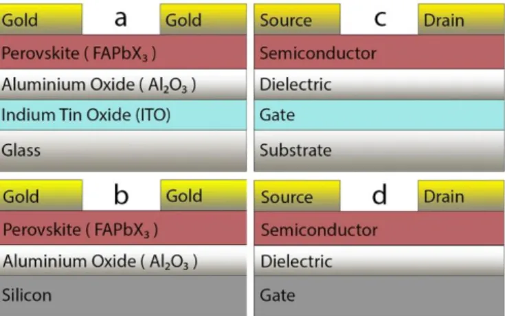
Next, thin-films were attached to an aluminium mask for gold deposition, creating both source and drain gold contacts. After this stage thin-film transistors fabrication was completed (fig.2.1). For ITO-based MOS capacitors, layering structure was the same except for the upper-contact which was made of aluminium.
Figure 2.1 - a), b) ITO and silicon TFT fabrication, respectively. c), d) ITO and silicon TFT layer functions.
2.3
Material Characterization
Perovskite characterization occurred during the following stages: perovskite liquid solutions, perovskite-only substrates, films with aluminium oxide and perovskite, and finally substrates with aluminium oxide, perovskite and gold contacts (being TFTs).
Liquid perovskite solutions were sent to TGA-DSC STA 449 F3 Jupiter machine for thermogravimetric analysis (TGA) under natural atmospheric conditions, in order to study the effect of thermal annealing on different samples.
Perovskite-only silicon and ITO-based glass substrates were sent to SEM Hitachi TM3030Plus scanning electron microscope (SEM), Ambios X-200 profilometer, Perkin-Elmer Lambda 950 spectrophotometer and X´Pert PRO X-ray Diffraction (XRD) machine, in order to study films chemical composition, thickness, absorbance and crystal structure type, respectively.
ITO-based glass substrates with aluminium oxide and perovskite were tested at HL55WIN Hall system and Keysight B1500A machine, for charge carrier properties and capacitance-voltage profile analyses, respectively. To allow for measurements, films at this point were coated with aluminium dots, being the upper-contacts. ITO served as gate bottom-contact.
TFTs of both ITO and silicon substrates were sent to Agilent 4155C semiconductor parameter analyzer to perform output and transfer curves.
9
3 Analysis of Results
This chapter concerns all characterization data regarding 𝐹𝐴𝑃𝑏𝐵𝑟𝑥𝐼3−𝑥 solutions and devices. Results appear according to material complexity, from perovskite solutions to thin-film transistors. Although 𝐹𝐴𝑃𝑏𝐵𝑟2𝐼1 based TFTs were not fabricated, these extra thin-films were produced in order to achieve a better understanding in film absorbance, thickness and morphology analysis, when varying bromine content. Films were fabricated in the same way as all the other 𝐹𝐴𝑃𝑏𝐵𝑟𝑥𝐼3−𝑥 perovskite thin-films.
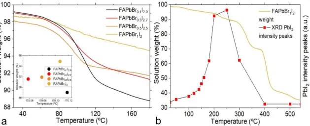
3.1 Thermal Gravimetric Analysis
Before thermal gravimetric measurement (TGA), four 𝐹𝐴𝑃𝑏𝐵𝑟𝑥𝐼3−𝑥 solutions were heated at 70ºC for 3 days to remove solvent excess. After heating treatment, liquid samples transformed into a gel-type were sent for TGA and thermally examined under standard atmospheric pressure. In-situ x-ray diffraction was also developed for comparison with 𝐹𝐴𝑃𝑏𝐵𝑟1𝐼2 mass weight percentage, also in the same environmental conditions.
All four solution mass weights are inversely proportional to increasing temperature. Moreover, for relatively high temperatures, samples with higher bromine content retain more mass weight than those with lesser bromine content, also, this weight percentage difference between samples becomes larger with increasing temperature [71-73]. These results suggest that bromine addition to solutions provides a higher structure stability when considering thermal annealing processes of 80ºC or more. Plus, special attention is given to weight percentage at 170ºC as it was the chosen temperature for thermal annealing of all thin-films (fig.3.1a). This analysis confirms ion Br
-thermal stability already discussed in sub-chapter 1.2, Perovskite materials.
Regardless of mass weight, reagents such as PbI2 can develop structure crystalline growth with
increasing temperature and/or overtime, the same way perovskite structures do [69,74-76]. However, after structures reach their maximum peak around 250ºC, the number of crystal structures abruptly decreases for a mass weight of 90%, suggesting no direct relation between mass loss and crystalline growth (fig.3.1b).
b
a
b
Figure 3.1 – a) Solution weight of samples with varied bromine content ( 0.1 ≤ x ≤ 1 ) as function of temperature heating. Inset graphic identifies more specifically weight percentage around 170ºC. b) Comparison between solution weight for and XRD impurity peaks for same 𝐹𝐴𝑃𝑏𝐵𝑟1𝐼2 sample, both as function of temperature annealing.
10
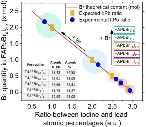
3.2 Energy-dispersive x-ray spectroscopy
Next to perovskite solution analyzes, thin-films were produced. In order to obtain a confirmation on samples chemical quantity, films were characterized via energy-dispersive x-ray spectroscopy (EDX) with SEM Hitachi TM3030Plus machine. Lead (Pb) and iodine (I) atomic percentages were collected. For bromine (Br), analysis was not possible because this element was inserted on a group of restricted elements for machine usage. Therefore, a ratio between atomic percentages of iodine and lead was made as an attempt for estimating bromine halide percentage in each sample. The expected bromine percentages were 3.33%, 10%, 16.67%, 33.33% and 66.67% for 𝐹𝐴𝑃𝑏𝐵𝑟0.1𝐼2.9, 𝐹𝐴𝑃𝑏𝐵𝑟0.3𝐼2.7, 𝐹𝐴𝑃𝑏𝐵𝑟0.5𝐼2.5, 𝐹𝐴𝑃𝑏𝐵𝑟1𝐼2 and 𝐹𝐴𝑃𝑏𝐵𝑟2𝐼1, respectively.
According to EDX data from recent literature, an inversely relation between the ratio of I and Pb atomic percentages and present bromine quantity is verified [77-78]. In the light of this suggestion, all produced films with lesser bromine quantity had lower bromine halide percentages than the expected (2.17%, 9.5%, 13% and 28.33% instead of 3.33%, 10%, 16.67% and 33.33%, respectively). The only exception was for the film with higher bromine content, having more percentage than the theoretically expected (72.89% instead of 66.67%) (fig.3.2).
Figure 3.2 – Bromine halide percentage in 𝐹𝐴𝑃𝑏𝐵𝑟𝑥𝐼3−𝑥 as a function of theoretical and experimental iodine - lead atomic percentage ratios. The blue dots represent the obtained samples and the orange rectangles are the ideally expected atomic ratio, and therefore the ideal bromine quantity. Both these symbols are surrounded by circles, each circle is related to a different perovskite composition. Inset table shows the experimentally obtained table by EDX analysis.
11
3.3 Absorbance analysis
Perovskite-only ITO-based glass thermal annealed substrates were subjected to absorbance and bandgap measures, calculated using transmittance data from Perkin-Elmer Lambda 950 spectrophotometer. Absorbance was directly obtained by Perkin Elmer machine and optical bandgap results were estimated using Tauc Plot method [79-82] for direct bandgap semiconductors [83-84]. Obtained results agreed with recent perovskite literature.
Regarding 𝐹𝐴𝑃𝑏𝐵𝑟𝑥𝐼3−𝑥 samples, all absorbance results demonstrate higher inconsistency at lower wavelengths (350𝑛𝑚 ≤ 𝜆 ≤ 440𝑛𝑚) and smaller peaks when increasing bromine content [85-86]. However, the latter films seem to retain a higher level of absorbance at bigger wavelengths (440𝑛𝑚 ≤ 𝜆 ≤ 600𝑛𝑚) (fig.3.3a). Plus, absorbance results at (𝜆 = 600𝑛𝑚) stabilize for (600𝑛𝑚 ≤ 𝜆 ≤ 2000𝑛𝑚).
When increasing bromine content to x = 2 (𝐹𝐴𝑃𝑏𝐵𝑟2𝐼2) absorbance stability increases among samples and peaks at lower wavelengths also slightly increase. Moreover, it’s possible to conclude that absorbance increases after thermal annealing process [87-88], meaning samples become denser (fig.3.3c).
Optical bandgap calculations for 𝐹𝐴𝑃𝑏𝐵𝑟𝑥𝐼3−𝑥 suggest film surface divergences, as according to literature data, three structure types were identified [89]. Regarding films tolerance factor and as explained in Introduction chapter, hexagonal structures suggest (t higher than 1), cubic structures (t around 1), tetragonal and orthorhombic structures (t lower than 1). Therefore, these films tolerance factor will be different from theoretical values presented in Introduction Chapter. Bandgap counting indicates the presence of mostly hexagonal structures (2𝑒𝑉 ≤ 𝐸𝑔 ≤ 2.5𝑒𝑉) which can be related to environment humidity [90-91], also, some of these twelve samples present two absorbance peaks (dual phase), possibly suggesting varied film thickness and therefore confirming the presence of more than one structure types. This may be related to precursors inadequate mixing during deposition process [65] (fig.3.3b).
For 𝐹𝐴𝑃𝑏𝐵𝑟2𝐼1 samples, results are quite different. Regardless of thermal annealing process, all eight samples present a dual phase which seem to correspond to orthorhombic structures (1.2𝑒𝑉 ≤ 𝐸𝑔 ≤ 1.45𝑒𝑉) and cubic structures (1.85𝑒𝑉 ≤ 𝐸𝑔 ≤ 1.65𝑒𝑉) [89].
As 𝑃𝑏𝐼2 reagent was not used to produce 𝐹𝐴𝑃𝑏𝐵𝑟2𝐼1 films, solution purity increased and risk of contamination diminished, also, more bromine incorporated seems to stabilize absorbance results. One of these reasons, or maybe both, is probably related to the equal quantity of present structures in 𝐹𝐴𝑃𝑏𝐵𝑟2𝐼1 films. Concerning thermal annealing, optical bandgaps slightly diminish after this process. (fig.3.3d).
Compared to recent literature, samples with lower bromine quantity (0.1 ≤ 𝑥 ≤ 1), present an absorbance profile similar to those of lead halides [92], 𝑀𝐴𝑃𝑏𝐼3 ambipolar hybrid phototransistors [93] and 𝑀𝐴𝑃𝑏𝐼3 solar cells [94]. Furthermore, for all samples (0.1 ≤ 𝑥 ≤ 2), as a bandgap increase is probably related to film polycrystallinity, films with lower bromine content (0.1 ≤ 𝑥 ≤ 1) are likely to have a higher number of polycrystalline structures when compared to 𝐹𝐴𝑃𝑏𝐵𝑟2𝐼1 sample structures [95].
12 Figure 3.3 - a), c) Absorbance of 𝐹𝐴𝑃𝑏𝐵𝑟𝑥𝐼3−𝑥 and 𝐹𝐴𝑃𝑏𝐵𝑟2𝐼1 samples as function of light wavelength. b, d) 𝐹𝐴𝑃𝑏𝐵𝑟𝑥𝐼3−𝑥 and 𝐹𝐴𝑃𝑏𝐵𝑟2𝐼1 tauc plot bandgap counting and identification of formed structures, according to literature.
3.4 Thickness measurement
Perovskite-only ITO-based glass thermal annealed substrates were thickness-analyzed by Ambios X-200 profilometer. Regarding films deposition, a small piece of kapton tape was added before spin-coating process to create one height step between substrate and perovskite film, thus facilitating profilometer measurement. Moreover, Swanepoel’s method of envelopes was introduced using Perkin Elmer transmittance data to estimate films thickness [96-98].
According to profilometer results, average thickness tends to increase for films with higher bromine content, which is in accordance with solar cells literature [99]. All films show thickness uncertainty regardless of bromine content, which can be related to the number of structure types present in samples, as discussed in Absorbance analysis sub-chapter. It is also important to refer that this uncertainty increases for samples with few bromine quantity, and then it gets smaller when adding a considerable amount of this cation (fig.3.4).
When comparing 𝐹𝐴𝑃𝑏𝐵𝑟0.1𝐼2.9 group of samples to the other groups, its uncertainty height is an exception, and this is probably due to the very low chemical quantity of present bromine, which is not enough to form bromine-based perovskite structures. This way less structure types are formed and thickness uncertainty decreases.
Regarding thickness calculation by transmittance data, the lowest calculated value from bottom envelops was 150nm and the highest value 296nm by upper envelops, establishing an estimate thickness region in accordance with the lower half of all profilometer thickness uncertainty bars.
a
b
c
13 Figure 3.4 - Film thicknesses of 𝐹𝐴𝑃𝑏𝐵𝑟𝑥𝐼3−𝑥 samples as function of bromine content ( 0.1 ≤ x ≤ 2 ). Brown rectangle represents Swanepoel’s thickness fitting [96-98].
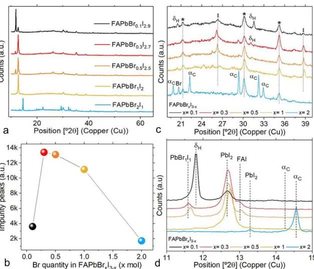
3.5 X-ray Diffraction
Perovskite-only ITO-based glass and silicon thermal annealed substrates were sent for x-ray diffraction (XRD) to analyze films crystallinity and purity. ITO-based substrates were all produced on the very same conditions, using same deposition process and a thermal annealing of 170ºC for 30min under vacuum. In-situ XRD technique was utilized to study samples thermal annealing process by varying time and temperature. Lastly, perovskite-only silicon-based substrates were also tested at XRD and used to compare films with different thermal annealing conditions.
3.5.1 ITO-based samples
When increasing bromine contents, it’s possible to identify a general horizontal peak shift and this is because bromine has a smaller lattice parameter than iodine, which shifts crystal structure peaks to higher angles [77]. Moreover, all 𝐹𝐴𝑃𝑏𝐵𝑟2𝐼1 peaks have lesser values of full width at half maximum (FWHM), meaning a higher number of crystal structures with a more precise lattice parameter (fig.3.5a).
Regarding XRD between 11º and 15º, two peaks are identified for x = 0.1. One very precise peak at 11.8º, which is related to perovskite yellow phase regarding hexagonal structures, and another peak around 12.6º suggesting the existence of 𝑃𝑏𝐼2 impurities [77,100] (corresponding to 𝛿H and 𝐼 symbols in fig.3.5, respectively). When adding few more bromine, yellow phase disappears, 𝑃𝑏𝐼2 impurities increase and 𝑃𝑏𝐵𝑟2 precursor reacts with part of 𝑃𝑏𝐼2, which is visible around 11.6º. The latter event suggests that, if both reagents react to each other only (𝑃𝑏𝐵𝑟1𝐼1) [101-102], a similar sized 𝐹𝐴𝐼 impurity, around 13º [103], also appears confirming a low or non-existent number of 𝐹𝐴𝑃𝑏𝐵𝑟𝑥𝐼3−𝑥 crystalline structures. However, when increasing bromine to x = 2, 𝐹𝐴𝐼 and 𝑃𝑏𝐵𝑟1𝐼1 impurities completely disappear, 𝑃𝑏𝐼2 impurity nearly disappears, and black phase (𝑎C symbol in fig.3.4) regarding cubic 𝐹𝐴𝑃𝑏𝐵𝑟𝑥𝐼3−𝑥 structures appears around 14.6º [77]. For x = 1, it was already possible to identify a black phase small peak around 14.3º (fig.3.5d).
In order to prove the diminishing of impurities, a sum of all impurity peaks intensity between 11º and 15º has been made as a function of bromine concentration (fig.3.5b).
XRD peaks between 20º and 40º were also specifically analyzed. It’s possible to visualize a gradual decrease in hexagonal phase and 𝑃𝑏𝐼2 impurity peaks (symbols) when increasing bromine content [77]. For x = 2, cubic or pseudo-cubic perovskite structures appear, 𝑃𝑏𝐼2 impurity totally or nearly disappears and a relatively small 𝑃𝑏𝐵𝑟2 impurity (𝐵𝑟 symbol in fig.3.4) forms around 20º. ITO peaks (* symbol in fig.3.4) don’t change much with bromine concentration, and,
14 just like all identified peaks written above, are in accordance with recent literature [77,104-106] (fig.3.5c).
Figure 3.5 - a) X-ray diffraction of 𝐹𝐴𝑃𝑏𝐵𝑟𝑥𝐼3−𝑥 samples with varied bromine content (0.1 ≤ x ≤ 2). b) Recorded intensity peak impurities in the range of 11 ≤ 2θ ≤ 15. c), d) X-ray diffraction zoom-in for same 𝐹𝐴𝑃𝑏𝐵𝑟𝑥𝐼3−𝑥 samples, concerning ranges of 20 ≤ 2θ ≤ 40 and 11 ≤ 2θ ≤ 15, respectively.
3.5.2 In-situ XRD
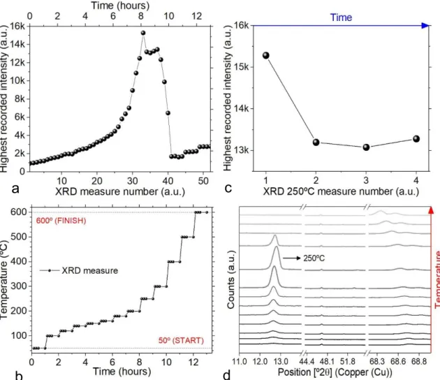
One perovskite-only silicon-based 𝐹𝐴𝑃𝑏𝐵𝑟1𝐼2 sample was sent for In-situ XRD in order to study both annealing time and temperature effects on crystallinity rate.
Sample was subjected to a non-vacuumed annealing of one hour per temperature, obtaining four XRD measures per hour and measuring along thirteen temperature levels within the range of 50ºC to 600ºC. For each temperature, first three measures were obtained during the first 30 minutes and the fourth measure was taken 30 minutes after the third measure (fig.3.6b).
Regarding all fifty-two measures, highest recorded intensities over time can be observed in fig.3.6a.
Concerning the highest peak, 𝑃𝑏𝐼2 impurity around 12.6º [77,100], annealing temperatures from 50ºC to 200ºC present higher intensity during their fourth measure, meaning temperature-time profile is appropriate until 200ºC. However, an increase in temperature (𝑇 ≥ 250º𝐶) confirms a gradual downfall on 𝑃𝑏𝐼2 crystallinity, taking place right after the appearance of the highest over-time recorded peak. The latter peak was obtained at 250ºC for 10 minutes, suggesting that similar temperature-time profiles should finish at this point, achieving the highest possible crystallinity (fig3.6c).
a
c
15 Moreover, another relevant XRD peak is identified near 68º with an increasing intensity proportional to temperature during all temperature-time profile. This peak, which was not identified for ITO-based glass 𝐹𝐴𝑃𝑏𝐵𝑟1𝐼2, suggests a silicon-based structure as it was no target of thermal degradation, actually the opposite [107-110]. Increasing intensity after measure number 40 is related to the appearance of this structure (fig.3.6a, d)
Figure 3.6 – a) XRD recorded intensity peaks during full temperature-time profile, obtaining a total of 52 measures. b) Temperature profile as function of sample thermal annealing. c) XRD recorded intensity peaks for 250ºC. d) XRD relevant 2θ positions vertically displaced as both intensity and annealing temperature functions.
3.5.3 Silicon-based samples
Silicon-based 𝐹𝐴𝑃𝑏𝐵𝑟1𝐼2 films were analyzed in order to study the effect of thermal annealing conditions in perovskite crystallinity. Silicon substrate was used instead of ITO-based glass to collect more results, also allowing for silicon and ITO comparison.
According to XRD results, samples annealed under vacuum conditions develop higher crystallinity and peaks with lesser FWHM [111-112], meaning a higher number of crystalline structures and with very similar lattice parameters. Plus, an inexistent peak at ITO-based 𝐹𝐴𝑃𝑏𝐵𝑟1𝐼2 appears around 60º for both silicon samples, suggesting a silicon-related crystal structure (fig.3.7a) [107-110].
Regarding XRD between 12.3º and 13.1º, both peaks suggest the existence of 𝑃𝑏𝐼2 impurity, as observed in ITO-based 𝐹𝐴𝑃𝑏𝐵𝑟1𝐼2 sample [77]. The horizontal shift concerning the non-vacuumed sample is probably related to precursors sensitivity to humidity, which according to perovskite literature is higher for iodine than bromine (fig.3.7c) [113].
a
c
16 Concerning silicon films, pictures were taken to both samples, vacuumed and non-vacuumed. A darker tone of color is observed for the vacuumed sample, which suggests a relation between film color intensity and crystallinity (fig.3.7b, d).
Figure 3.7 – a) Overall XRD profile comparison between vacuumed sample (red line) and non-vacuumed sample (black line). c) XRD zoom-in on 12.3º ≤ 2𝜃 ≤ 13.3º regarding 𝑃𝑏𝐼2 impurity peaks for both samples. b), d) Surface colorimetric differences between both samples, suggesting an overall darker tone for the vacuumed sample.
Regarding silicon samples, standard annealing process was also compared to In-situ annealing. Two silicon based 𝐹𝐴𝑃𝑏𝐵𝑟1𝐼2 samples, both annealed under standard atmospheric pressure, were subjected to different annealing treatments and place side by side at XRD examination. Visualizing XRD graphics, it´s possible to detect two higher peaks around 12.7º which concerns same 𝑃𝑏𝐼2 impurity already discussed (fig.3.8b) [77,100]. This impurity represents the only peak lower for In-situ XRD sample when compared to standard annealed sample, as all the other peaks are more intensive and have lesser FWHM for the In-situ case (fig.3.8a).
Moreover, a horizontal shift to higher angles happens for standard annealed sample which is probably related to silicon substrate, as ITO-based samples subjected to the same standard process don’t present these shift on peaks with this level of intensity. These results suggest silicon possibly requires more annealing time than ITO-based glass substrates (fig.3.8b, c, d).
17 Overall, impurities and degradation verified for some ITO and silicon samples, are possibly related to the effective time used for thermal annealing process, as pointed out by one research concerning annealing effects on 𝐹𝐴𝑃𝑏𝐼3 solar cells [114]. Plus, and regarding ITO samples only, the contrasting thermal expansions of perovskite and Indium-tin oxide can contribute to a faster perovskite degradation [115].
3.6 Charge-carrier properties
ITO-based glass samples with semiconductive and conductive layers, perovskite (𝐹𝐴𝑃𝑏𝐵𝑟𝑥𝐼3−𝑥) and aluminium coverage, respectively, were tested at HL55WIN Hall effect machine for charge-carrier properties analysis. Values of charge-carrier concentation, mobility and resistivity were obtained for films with different bromine contents (0.1 ≤ 𝑥 ≤ 1). Due to program error, some mobility and resistivity values were not recorded by the computer. Yet, all charge concentration values either n-type or p-type were properly displayed.
According to concentration data, p-type nature is identified for 𝐹𝐴𝑃𝑏𝐵𝑟0.1𝐼2.9 and 𝐹𝐴𝑃𝑏𝐵𝑟0.5𝐼2.5 samples, whereas n-type is obtained for all studied samples. It’s possible to conclude that, for low bromine content (𝑥 = 0.1), all concentration values present very large mean deviation, meaning an overall divergence from both n-type and p-type averages. Increasing bromine content (𝑥 ≥ 0.1) results in much higher concentration averages and lesser mean deviations. Moreover, for sample 𝐹𝐴𝑃𝑏𝐵𝑟0.5𝐼2.5 n-type and p-type concentrations are very similar suggesting ambipolar characteristics (charge transport of both electrons and holes), as positive and negative values were obtained in different trials for the same thin-film (fig.3.9a).
a
b
c
d
Figure 3.8 – a) XRD peaks comparison between standard annealing and In-situ XRD annealing of 𝐹𝐴𝑃𝑏𝐵𝑟1𝐼2 samples. b), c), d) XRD zoom-in for both samples regarding peaks within the ranges of 12.3º ≤ 2𝜃 ≤ 13.1º, 65º ≤ 2𝜃 ≤ 75º and 30º ≤ 2𝜃 ≤ 41º
18 Regarding data with associated resistivity and mobility, all resistivity values diminish when increasing bromine to 𝑥 = 0.3 and stabilize for 0.3 ≤ 𝑥 ≤ 1. Mobility values increase with ascending bromine content. These values, being very similar for both n-type and p-type mobilities, also suggest sample ambipolarity and are relatively high when compared to recent perovskite literature (fig.3.9b). The latter describes a recorded maximum p-type mobility of 15𝑐𝑚2/𝑉𝑠 and n-type mobility of 27𝑐𝑚2/𝑉𝑠 for polycrystalline thin-films produced in the very same conditions and materials [116-118]. Plus, for relatively similar perovskites ((𝐹𝐴𝑃𝑏𝐼3)1−𝑥(𝑀𝐴𝑃𝑏𝐵𝑟3)𝑥), p-type and n-type mobilities of 20 ± 8 𝑐𝑚2/𝑉𝑠 and 17 ± 9 𝑐𝑚2/𝑉𝑠, respectively, were presented in another research [119]. In this work, maximum achieved mobilities were 20.2𝑐𝑚2/𝑉𝑠 for p-type and 38𝑐𝑚2/𝑉𝑠 for n-type.
Overall, here all studied concentration, mobility and resistivity properties stabilize for higher bromine contents (𝑥 ≥ 0.1). All recorded hall mobility values suggest the presence of mostly polycrystalline structures, as single-crystal mobility is generally 10 times higher (or more) than the former structures [120-121].
Figure 3.9 – a) Charge concentration with bromine content variation. b) Thin-flms associated carrier mobility, resistivity and charge concentration.
When obtaining hall mobility, structural information such as thin-film crystalline nature can be estimated by calculating diffusion coefficient 𝐷𝐶. The latter coefficient is directly obtained from the recorded mobility, and when multiplied by the average carrier lifetime (defined as the time a minority charge takes to recombine) it provides the squared value of average carrier diffusion length, the distance completed by a particle before its recombination with a carrier of the opposite charge. For the following analyses, 𝐹𝐴𝑃𝑏𝐵𝑟0.1𝐼2.9 sample with n-type hall mobility of 27.1𝑐𝑚2/𝑉𝑠 is assumed to be one 𝐹𝐴𝑃𝑏𝐼3 substrate, because mobility value is exactly the same according to literature [116], and, as discussed in Absorbance analysis and X-ray diffraction sub-chapters, films with very low bromine content have higher chances of not developing any bromine structures at all.
Diffusion coefficient values were obtained directly from hall mobility, whereas carrier lifetime, that can be analyzed via time-resolved photoluminescence spectroscopy [122], was not done during laboratory work. Therefore, using literature information on 𝐹𝐴𝑃𝑏𝑋3 carrier lifetime 𝑡𝐶 and diffusion length 𝐷𝐿, theoretical diffusion coefficients were calculated using organic semiconductor formula (𝐷𝐿= √𝐷𝐶𝑡𝐶) and related to 𝐷𝐶 values obtained during this work. Plus, as single crystal and polycrystalline films generally present different carrier lifetime 𝑡𝐶 (and therefore different diffusion lengths) [123], literature information was also compared to thin-film coefficients as an attempt to understand the crystalline structures of films developed in this work.
Interestingly, when increasing bromine content, experimental diffusion coefficients approach a theoretical 𝐹𝐴𝑃𝑏𝑋3 single-crystal profile instead of polycrystalline profile, according to the suggested carrier lifetime ranges (usually 100𝑛𝑠 ≤ 𝑡𝐶 ≤ 1000𝑛𝑠 for polycrystalline and 400𝑛𝑠 ≤
19 𝑡𝐶 ≤ 4000𝑛𝑠 for single-crystal). Furthermore, when relating the diffusion coefficient 𝐷𝐶 of 𝐹𝐴𝑃𝑏𝐼3 (𝐷𝐶 = 0.70𝑐𝑚2/𝑠, for sample with 27𝑐𝑚2/𝑉𝑠 mobility) with theoretical carrier lifetime, a diffusion length of 6.45𝑢𝑚 is achieved which is similar to single-crystal’s 𝐹𝐴𝑃𝑏𝐼3 literature data of about 6.60𝑢𝑚 (fig.3.10a) [124]. These results are the opposite of those suggested by hall mobility. Probably meaning that, samples are for all purposes, polycrystalline, however displaying single-crystal characteristics such as higher carrier lifetimes and diffusion lengths [125].
Moreover, and according to recent literature, an inversely relation between carrier mobility and lifetime is verified for organic photovoltaics. This information can probably contradict the previous conclusions on samples crystal structures, as obtained polycrystalline hall mobilities are relatively high and therefore the respective carrier lifetimes would be low [126]. However, this is not conclusive as another study, based on halide perovskites, suggests a direct relation between carrier lifetime and thermal annealing time [122]. Samples for this work were annealed during 30min, which is considered a relative high time.
According to time-of-flight method for organic semiconductors, thin-film charge transit time (the time device takes to respond) can be obtained when knowing the values of carrier mobility and separation distance between contacts [127-129]. Therefore, mobility values were obtained and the distance between the four electrodes was verified to be the same during all measurements, of about 1cm. Along with transit time calculations, another studied factor was the hall contact voltage, resulting as a voltage average measured between all the contacts. Concerning this data, when lifting carrier mobility (either n-type or p-type), charge transit time diminishes and average contact voltage increases (fig.3.10b).
Figure 3.10 – a) Comparison between diffusion coefficient values directly obtained from hall effect mobilities (horizontal bands) and diffusion coefficient values of literature data (FAPbI3 being the black dots and FAPbBr3 the blue dots), providing a relation between carrier diffusion and expected range of carrier lifetime for both single crystal and polycrystalline films [123-124]. b) Charge transit time and average hall contact voltage, both as a function of carrier mobility [127-129]
3.7 Capacitance measurement
ITO-based glass metal-oxide-semiconductor (MOS) capacitors with dielectric, semiconductive and conductive layers, aluminium oxide (𝐴𝑙2𝑂3), perovskite (𝐹𝐴𝑃𝑏𝐵𝑟𝑥𝐼3−𝑥) and aluminium coverage, respectively, were tested at Keysight for capacitance analysis.
Concerning voltage terminals, a small thin-film area was covered with kapton tape during layers deposition in order to allow ITO intact gate surface. Perovskite coverage with small aluminium dots was made for creation of the source, the upper contact. Since data errors occurred for some of the measurements, probably due to leakage current or bad electrical contact, only 𝐹𝐴𝑃𝑏𝐵𝑟0.1𝐼2.9 and 𝐹𝐴𝑃𝑏𝐵𝑟0.5𝐼2.5 samples were successfully analyzed.
![Figure 1.3 - Framing of perovskite examples in a tolerance factor versus octahedral factor mapping [20] with recent effective radius values for the organic cations [32, 47]](https://thumb-eu.123doks.com/thumbv2/123dok_br/15468720.1033518/25.892.237.656.782.1115/figure-framing-perovskite-examples-tolerance-octahedral-mapping-effective.webp)
![Figure 1.4 - a) Metal-oxide-semiconductor-field-effect-transistor layering structure and b) thin-film-transistor layering structure [52]](https://thumb-eu.123doks.com/thumbv2/123dok_br/15468720.1033518/26.892.131.763.754.928/figure-semiconductor-transistor-layering-structure-transistor-layering-structure.webp)
![Figure 1.5 – a) Current-voltage curve for measuring perovskite power conversion efficiency (PCE) comparing one-step to two-step spin methods [61]](https://thumb-eu.123doks.com/thumbv2/123dok_br/15468720.1033518/27.892.132.764.575.801/figure-current-voltage-measuring-perovskite-conversion-efficiency-comparing.webp)