1
Boosting Electrical Performance of High
‑κ Nanomultilayer Dielectrics
2
and Electronic Devices by Combining Solution Combustion Synthesis
3
and UV Irradiation
4
Emanuel Carlos, Rita Branquinho,
*
Asal Kiazadeh, Jorge Martins, Pedro Barquinha, Rodrigo Martins,
5and Elvira Fortunato
*
6CENIMAT/i3N Departamento de Ciência dos Materiais, Faculdade de Ciências e Tecnologia (FCT), Universidade NOVA de Lisboa
7 (UNL), and CEMOP/UNINOVA, 2829-516 Caparica, Portugal
8
*
S Supporting Information9 ABSTRACT: In the past decade, solution-based dielectric 10 oxides have been widely studied in electronic applications
11 enabling the use of low-cost processing technologies and
12 device improvement. The most promising are the high-κ
13 dielectrics, like aluminum (AlOx) and hafnium oxide (HfOx), 14 that allow an easier trapfilling in the semiconductor and the 15 use of low operation voltage. However, in the case of HfOx, a 16 high temperature usually is needed to induce a uniform and
17 condensed film, which limits its applications in flexible
18 electronics. This paper describes how to obtain HfOxdielectric 19 thinfilms and the effect of their implementation in multilayer 20 dielectrics (MLD) at low temperatures (150°C) to apply in 21 thinfilm transistors (TFTs) using the combination of solution
22 combustion synthesis (SCS) and ultraviolet (UV) treatment. The single layers and multilayers did not show any trace of residual 23 organics and exhibited a small surface roughness (<1.2 nm) and a high breakdown voltage (>2.7 MV cm−1). The resulting TFTs 24 presented a high performance at a low operation voltage (<3 V), with high saturation mobility (43.9± 1.1 cm2V−1s−1), a small 25 subthreshold slope (0.066± 0.010 V dec−1), current ratio of 1× 10⁶and a good idle shelf life stability after 2 months. To our 26 knowledge, the results achieved surpass the actual state-of-the-art. Finally, we demonstrated a low-voltage diode-connected
27 inverter using MLD/IGZO TFTs working with a maximum gain of 1 at 2 V.
28 KEYWORDS: low temperature, nanomultilayer dielectric oxides (AlOxand HfOx), DUV irradiation, solution combustion synthesis,
29 low operating voltage TFTs
1. INTRODUCTION
30Technology has been growing exponentially, leading to the 31necessity of low-cost processes and materials that allow a more 32sustainable world. For that, printable, flexible, disposable, and 33transparent electronics have been highly explored.1,2However, 34the typical fabrication techniques for oxidefilms and devices are 35vacuum-based techniques, like atomic layer deposition and
36chemical and physical vapor deposition. These techniques
37require expensive high-vacuum equipment, resulting in high 38production costs.1 For the production of printed electronics, 39suitable materials and optimized processes or techniques with 40low-cost manufacturing need to be identified and developed. As 41a result, solution-based thinfilms have gained a lot of attention 42due to the low cost, simplicity and goodfilm uniformity in large 43areas.3 Spin-coating, screen printing, inkjet printing, bar-44coating, and spray pyrolysis are the most-used techniques for 45solution processing oxide semiconductors and gate dielec-46trics.3−7Actually, choice of suitable functional/active materials 47that can be printed is essential for the performance of the
48printed electronic devices. In thin film transistors, the
49
semiconductor layer has been used in organics and inorganics
50
(oxides) with high success at low temperature.8,9
51
The insulator layer plays a crucial role in the devices
52
performance too, by mainly defining the devices stability and
53
operation voltages.8−11Also, the solution process of this layer
54
has been frequently used, either for organics or oxides
55
materials. In the case of organic materials, PVA or PVP are
56
possible alternatives;12−14however, these have some setbacks,
57
such as the operation voltage control with the decrease in
58
thickness, low carrier mobility, and instability issues, which limit
59
their application.8,9,11By using solution-based high-κ inorganic
60
dielectrics is possible to enhance the capacitance coupling
61
between the gate dielectric and the channel layer in TFTs. As a
62
result, the subthreshold slope is improved and the operating
63
voltage is reduced leading to low consumption electronic
64
devices.15,16 Moreover, the use of multilayers allows the
Received: August 7, 2017
Accepted: November 1, 2017
Published: November 1, 2017
Research Article
www.acsami.org
© XXXX American Chemical Society A DOI:10.1021/acsami.7b11752
65insulator to achieve remarkable properties with just one 66material (e.g., high-κ and band gap).17,18 The most used 67inorganic dielectrics are zirconium oxide (ZrO2), tantalum 68oxide (Ta2O5), aluminum oxide (Al2O3), hafnium oxide 69(HfO2) and their mixtures.3,17,19−21 The larger capacitance 70obtained with these allows a higher density of charges induced 71in the semiconductor, which lead to an easier trap filling. 72Solution-processed Al2O3 and HfO2 are the most promising 73candidates, with high dielectric constant, 9 and 25 respectively,
74and in the case of HfO2 a lower bandgap (5.8 eV) when
75compared with Al2O3 (8.9 eV).11,15 Because the bandgap is 76smaller in the case of HfO2, the carrier injection is easier than in 77Al2O3.17,22 However, these materials needed high annealing
78temperatures, so new methods and techniques have been
79developed, like solution combustion synthesis (SCS) and deep 80ultraviolet (DUV) treatment, to obtain high-qualityfilms at low
81temperature that are compatible with low-cost flexible
82substrates.8,9 In the case of SCS, an oxidizer (nitrates) and a 83fuel (urea, citric acid) are added to the precursor solution. 84During the annealing process a exothermic reaction occurs, 85resulting in a reduction of the external heat required for thefilm
86formation; the remove of organic solvents and film
87densification.9,19 By using a DUV treatment, the films are 88exposed to high-energy photons, which causes the cleavage of 89alkoxy groups, active metals, and oxygen atoms to simplify M−
90O−M network formation. After less than 10 min of UV
91irradiation, the polymeric chains break into smaller fragments,
92which induces degradation, leading to removal of oxygen,
93carbon and improving the film densification.11,23,24 The 94combination of these methods improves the reliability of the 95nanoscale film morphology, composition of metal oxides and 96stability over time. The additional energy provided by the 97exothermic combustion reaction contributes to enhanced film 98densification in a short annealing time.
99 In this work, we report for the first time the combination 100between the solution combustion synthesis (SCS) and deep 101ultraviolet (DUV) treatment in HfOxsingle and nanomultilayer 102dielectrics (composed by AlOx and HfOx thin films) at low 103temperature (150 °C) in gallium-indium-zinc oxide (IGZO)
t1 104TFTs (Table 1). The effects of increasing the number of
105dielectric layers in the electric performance were investigated 106using different characterization techniques. Finally, stable and 107low voltage (HfOx|HfOx)/IGZO TFTs have been applied to a 108diode-connected inverter.
2. EXPERIMENTAL DETAILS
109
2.1. Precursor Solution Preparation and Characterization.
110
Aluminum nitrate nonahydrate (Al(NO3)3·9H2O, Fluka, 98%) was
111
dissolved in 2-methoxyethanol (2-ME, C3H8O2, ACROS Organics,
112
99%), to yield solution with an Al3+ion concentration of 0.1 M. Urea
113
(CO(NH2)2, Sigma, 98%) was then added to the prepared solution
114
which was maintained under constant stirring for at least 1 h. The urea
115
to aluminum nitrate molar proportion was 2.5:1, to guarantee the
116
redox stoichiometry of the reaction.19 Hafnium chloride-based
117
precursor (HfCl4, Alfa Aesar, 99.9%) was dissolved in
2-methox-118
yethanol (2-ME, C3H8O2, ACROS Organics, 99%) and maintained
119
under constant stirring for 4 h. Then the oxidizing agent, ammonium
120
nitrate (NH4NO3, Roth, 98%) and the fuel, urea was added and stirred
121
at least 2 h for a concentration of 0.1 M. For the ammonium nitrate
122
precursor, the urea molar proportion was 1:(1/3). All precursor
123
solutions werefiltrated through 0.20 μm hydrophilic filters before use.
124
The precursor’s solvent evaporation with a rotatory evaporator
125
(Heidolph, model Hei-VAP Value/G3) was done before the
126
thermogravimetry and differential scanning calorimetry (TG-DSC)
127
at 70°C with a rotation of 50 rpm during 1 h 30 min. A thermal
128
characterization of precursors was then performed by TG-DSC under
129
air atmosphere up to 500°C with a 10 °C min−1heating rate in an
130
aluminum crucible using a simultaneous thermal analyzer, Netzsch
131
(TG-DSC - STA 449 F3 Jupiter). The optical properties were
132
obtained using a PerkinElmer lambda 950 UV/vis/NIR
spectropho-133
tometer by measuring absorbance (A) in the wavelength range of
134
190−400 nm.
135
2.2. Dielectric Deposition and Characterization. Prior to
136
deposition all substrates (silicon wafer and corning glass with an area
137
of 2.5 × 2.5 cm2) were cleaned in an ultrasonic bath at 60 °C in
138
acetone for 10 min, then in 2-isopropanol for 10 min and dried under
139
nitrogen (N2); followed by a 10 min UV/Ozone surface activation step
140
in a PSD-UV Novascan system. Thin films were deposited by spin
141
coating, forming a single layer (AlOx; HfOx) and multilayers (AlOx|
142
HfOx; AlOx|HfOx|AlOx; HfOx|HfOx; HfOx|AlOx; HfOx|AlOx|HfOx)
143
using the AlOxand HfOxprecursor solutions with a concentration of
144
0.1 M for 35 s at 2000 rpm (Laurell Technologies). That was followed
145
by an immediate thermo annealing at 150°C assisted by ultraviolet
146
irradiation (UV) (PSD Pro Heated Series, PSDP-UVT Novascan
147
system; emission wavelengths of 253.7 (90%) and 184.9 nm (10%);
148
area of 20× 20 cm2) at a lamp distance of 2 cm (the output energy
149
intensity of the lamp was 75 mW·cm−2at 254 nm) for 30 min each
150
layer in nitrogen ambient, with a gas flow of 240 mbar. The filmś
151
structure was assessed by glancing angle X-ray diffraction (GAXRD)
152
performed by an X’Pert PRO PANalytical powder diffractometer using
153
Cu Kα line radiation (λ = 1.540598 Å) with an angle of incidence of
154
the X-ray beamfixed at 0.9°. The surface morphology was investigated
155
by atomic force microscopy (AFM, Asylum MFP3D) and the film
156
thickness by scanning electron microscopy analysis of a sample
cross-157
section prepared by focused ion beam using Ga+ions (SEM-FIB, Zeiss
Table 1. Literature of Developed High-κ Solution-Based Hafnium Oxide Single Layers and Multilayers Applied in TFTs
Year TFT (dielectric/semiconductor) T (°C) SS (V dec−1) μSAT(cm2V−1s−1) I
ON/OFF VON(V) VGrange (V)
201217 (HfOx|AlOx)/ ZTO 400 0.12 3.8 1× 10⁵ 0.4 −2 to 3
(AlOx|HfOx)/ ZTO 0.16 1.2 −0.2
201225 (HfO x)/ZTO 300 0.11 1.1 1× 10⁷ 0.2 −5 to 5 201526 (HfOx)/HIZO 500 1.1 3.6 1× 10⁴ −0.1 - 5−10 201527 (HfO x)/ZnO 380 42± 1.4 1× 10⁷ −0.4 −1 to 6 201516 (HfOx)/IZO 300 0.72 25.7 1× 10⁶ 1.5 −1 to 5 200 1.32 6.2 1× 10³ 0.8 201715 (HfO x)/ZTO 350 0.07 13.2 1× 10⁸ −0.1 −1−2
present study (HfOx)/IGZO 150 0.082± 0.002 31.2± 1.4 1× 10⁵ −0.04 ± 0.05 −1−2
(HfOx|HfOx)/ IGZO 0.066± 0.010 43.9± 1.1 1× 10⁶ 0± 0.03 −1−2
(HfOx|AlOx)/ IGZO 0.076± 0.009 23.6± 0.6 1× 10⁵ 0.01± 0.03 −1−2 (HfOx|AlOx|HfOx)/IGZO 0.101± 0.004 37.5± 2.2 0.03± 0.06 −1−3
(AlOx|HfOx)/IGZO 0.099± 0.019 37.2± 1.9 −0.01 ± 0.06 −1−2
(AlOx|HfOx|AlOx)/IGZO 0.133± 0.013 30.5± 1.8 −0.09 ± 0.09 −1−3
DOI:10.1021/acsami.7b11752
ACS Appl. Mater. Interfaces XXXX, XXX, XXX−XXX
158Auriga Crossbeam microscope). Fourier Transform Infra-Red (FTIR)
159spectroscopy characterization of thinfilms deposited on Si substrates
160data were recorded using an attenuated total reflectance (ATR) 161sampling accessory (Smart iTR) equipped with a single bounce
162diamond crystal on a Thermo Nicolet 6700 Spectrometer. The spectra
163were acquired with a 45° incident angle in the range of 4500−540 164cm−1and with a 4 cm−1resolution.
165 2.3. Electronic Device Fabrication and Characterization.
166Metal−insulator−semiconductor (MIS) capacitors were produced by
167depositing a single layer, AlOxor HfOx, and multilayers onto p-type
168silicon substrates (1−10 Ω·cm) as described above. Aluminum 169electrodes (80 nm thick) with an area of 1.96 × 10⁻³ cm2 were
170deposited by thermal evaporation via shadow mask on top of the
171insulators, with similar but unpatterned electrodes being also
172deposited on the back of the silicon wafer. Electrical characterization
173was performed measuring both the capacitance−voltage and
174capacitance-frequency characteristics in the range of 1 kHz to 1
175MHz of frequency using a semiconductor parameter analyzer
176(Keithley 4200SCS) and probe station (Janis ST-500). The TFTs
177were produced in a staggered bottom-gate, top-contact structure by
178depositing the single layers or the nanomultilayers onto p-type silicon 179substrates acting as gate electrodes.
180 The IGZO semiconductorfilm (30 nm thick) was sputtered onto
181the dielectric thin films via shadow mask for all temperatures. The
182deposition was performed using a commercial IGZO ceramic target
183(2:1:2 In:Ga:Zn atomic ratio) by rf magnetron sputtering in an Ar+O2
184atmosphere without intentional substrate heating in an AJA 1300-F
185system.28
186 Finally, source and drain aluminum electrodes (80 nm thick) were
187deposited by thermal evaporation via shadow mask onto the films.
188Hereafter the IGZO TFTs were annealed at 150°C, for 1 h in air. An
18980 nm thick aluminum film was also deposited on the back of the
190silicon wafer.
191 The current−voltage characteristics of the devices were obtained in 192double sweep mode in ambient conditions using a semiconductor
193parameter analyzer (Agilent 4155C) attached to a microprobe station
194(Cascade M150) inside a dark box, at room temperature.
195 The saturation mobility (μSAT) was determined from the following
196equation μ =⎛ − ⎝ ⎜ ⎞ ⎠ ⎟ I C W L V V 2 ( ) D ox SAT G T 2 197 (1)
198where Coxis the gate dielectric capacitance per unit area, the channel
199length (L) and width (W) are 90 and 1000μm, VGis the gate voltage,
200and VT is the threshold voltage, which was determined in the
201saturation region by linearfitting of a ID1/2vs VGplot.
202 Gate bias stress tests were performed on TFTs with one and two
203layers of dielectric under air environment by applying a constant gate
204voltage (0.5 MV cm−1electricfield) for 1 h, after which the devices
205were allowed to recover. Transfer characteristics were measured at
206fixed time intervals during stress and recovery processes.
207 To investigate the possibility of solution-based TFTs in circuit
208application, we constructed the inverter structure with two TFTs in
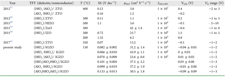
209different substrates. A semiconductor parameter analyzer (Keysight
210B1500A) was used for the DC characterization of the inverter. For
211transient measurements of the inverter, the input waveforms were
212generated by a function generator (Wavetek 395) and the output
213signal was acquired by an oscilloscope (ISO-TECH IDS 8062).
3. RESULTS AND DISCUSSION
214Solution combustion synthesis of nanomaterials has been
215crucial for the fabrication of high-quality metal oxides at low 216temperature.9In combustion synthesis at certain temperature, a 217violent redox reaction between an organic fuel, urea, and the 218oxidizer, ammonium nitrate, occurs, related with the release of 219massive reaction heat. This local heat results in the increase of 220local temperature inside the dielectric films, which promotes 221the precursors conversion into oxides at low temperature.19
222
Since 2011, the solution combustion synthesis of AlOx thin 223
films applied in TFTs has been reported; however, for HfOx, 224
only a few results have succeeded with high-performance TFTs
225
requiring high temperatures (Table 1).9,15,29
226
The solution combustion synthesis of HfO2 from hafnium 227
chloride and ammonium nitrate (oxidizer), and urea (reducing
228
agent) can be represented by the combination of ammonium
229
nitrate decomposition reaction (eq 2) and urea oxidation
230 reaction (eq 3). + → + + + HfCl4 4NH NO4 3 HfO2 6H O2 4N2 4HCl 231 (2) +⎜⎛ ⎟ → + + ⎝ ⎞⎠ CO(NH ) 3 2 O 2H O CO N 2 2 2 2 2 2 232 (3) 233
The overall reaction can thus be written as bellow (eq 4):
+ + → + + + + 3HfCl 12NH NO 4CO(NH ) 3HfO 16N 4CO 26H O 12HCl 4 4 3 2 2 2 2 2 2 (4) 234 235
This is a theoretical reaction equation that neglects possible
236
secondary reactions, although, it allows the calculation of a
237
stoichiometric condition that can be used as a reference.30In
238
the oxide formation, the chemistry of the redox reaction is
239
determinant for the thermodynamics, particularly, the nature of
240
the reagents and the fuel/oxidizer (ϕ).30
241
The optimal stoichiometry composition of the redox mixture
242
is obtained forϕ = 1; however, to achieve lower temperatures
243
in the thin film formation, as shown by DSC-TG analysis
244 f1
(Figure 1a), was usedϕ = 1.1. In this composition, the redox
245
mixture is under fuel-rich condition, requiring molecular
246
oxygen to fully convert the fuel.31,32 The oxidizing/reducing
247
characteristics of a mixture can be calculated by the Jain
248
method, which is based on propellant chemistry.33 In this
Figure 1. (a) TG-DSC analysis of HfOxprecursor solution and (b)
absorbance spectra of both AlOxand HfOxprecursor solutions. DOI:10.1021/acsami.7b11752
ACS Appl. Mater. Interfaces XXXX, XXX, XXX−XXX
249method carbon and hydrogen are considered as reducing 250elements withfinal valences of +4 and +1, respectively; hafnium 251metal ions are also considered reducing elements with a final 252valence of +4. Oxygen and nitrogen are considered oxidizers 253with theirfinal valences of −2 and 0, respectively. The reducing 254valence of urea is +6 and the oxidizing valence of ammonium 255nitrate is−2 as calculated by the Jain method hence (1/3) mol
256of urea are required per mole of the nitrate precursor
257(ammonium nitrate) to ensure redox stoichiometry. In this 258condition, to minimize the generation of cracks and pores in 259metal oxidefilms, which can significantly contribute to leakage 260current in the vertical direction, deep ultraviolet (DUV) 261treatment was used.8,10The condensation and film densifica-262tion in metal oxides are improved with DUV irradiation in 263nitrogen environment; however, some ozone (O3) is also 264formed, which in this case helps to fully convert the fuel in the 265combustion reaction at low temperatures.
266 3.1. Precursor Solution Characterization. Thermal
267analysis of precursor solutions was performed to investigate 268the decomposition behavior of the hafnium oxide precursors 269with different stoichiometry compositions.Figure 1a shows the 270differential scanning calorimetry (DSC) and thermogravimetry 271(TG) of the HfOxup to 350°C, as above this temperature no 272further events were observed. The most promising precursor 273solution with a fuel rich condition,ϕ = 1.1, exhibits an intense 274exothermic peak at 221°C and small peak at 304 °C, which is 275attributed to the combustion reaction of residual fuel resulting
276in a mass loss of 40%. Also, two endothermic peaks were
277observed at 139 and 172 °C, which are related to the solvent 278evaporation and some residual organics. In the case of the 279stoichiometry condition,ϕ = 1, the precursor solution show a 280smaller exothermic peak at 232°C and the most intense one at 281273°C, which is higher than the fuel rich condition. Thermal 282analysis indicates that the minimum temperature required for 283full degradation is 304°C. The DSC-TG analysis 2-ME based 284of AlOx precursor solutions, has been previously reported by 285our group,34and shows an intense exothermic peak at 176°C 286corresponding to oxide formation, and a residual endothermic 287peak at 250 °C attributed to the degradation of residual 288organics. The difference in combustion reaction temperature of 289HfOx and AlOx is expected as it depends on the specific 290bonding energy of the ligands with the metal ions in solution 291which varies from metal to metal, as reported by Epifani et al.35
292 The absorbance of the precursor solutions in the UV−vis
293range was performed to assess the efficiency of irradiation with
294a DUV lamp with a maximum emission at 254 nm (90%) to
295enhance film condensation and densification.8,24 Figure 1v 296shows that both solutions absorb in that wavelength, being 297more significant for the hafnium oxide precursor solution.
298Therefore, DUV treatment is expected to contribute to
299degradation of organic residuals and decreasing the temperature 300required for the formation of M-O-M.8
301 3.2. Dielectric Thin Film Characterization. The optical
302transmission of single and multilayer thinfilms was measured. f2 303Figure 2shows that all films are highly transparent (>89%) in 304the visible range. However, with an increase in the number of 305layers and film thickness, total transmittance is slightly 306decreased. The optical bandgap (Eg), determined via Tauc 307plot analysis is 4.9 eV for HfOxthinfilms, as shown inFigure 2. 308This value is lower than the expected 5.8 eV reported for 309physical vapor deposition (PVD) techniques.15,22 HfOx thin 310films produced by solution may have some residual chloride
311species which slow down the dehydroxylation process and
312
increase the amount of oxygen vacancies in the thinfilm, which
313
results in a decrease of the bandgap energy due to the
314
increasing of density of states.15 The bandgap of the other
315
layers was not obtained because of the presence of aluminum
316
oxide, which has a large bandgap (8.9 eV) unable to be
317
measured using Tauc plot analysis.36
318
The dielectric thin films produced were characterized with
319 f3
ATR-FTIR before and after annealing, as shown in Figure 3a.
320
All samples show an absorbance peak at 1107 cm−1attributed
321
to the Si−O transversal optic stretching.
322
Prior to annealing absorption bands related to organic
323
precursors in thefilm can be observed, namely, a broad band
324
between 3700 and 3000 cm−1 and bands at 1630 and 1575
325
cm−1 assigned to O−H stretching vibrations associated with
326
water absorption and OH increase; weak absorption bands
327
between 3090 and 2800 cm−1associated with the C−H stretch Figure 2.Optical transmittances of the single and multilayer dielectric thinfilms. The inset shows the Tauc plot of HfOx.
Figure 3.(a) FTIR spectra of AlOxand HfOxthinfilms before and
after annealing; (b) XRD diffractograms, AFM deflection images (1 × 1 μm2) of both dielectric thin films, and high-resolution SEM-FIB
cross-section image of HfOxthinfilm.
DOI:10.1021/acsami.7b11752
ACS Appl. Mater. Interfaces XXXX, XXX, XXX−XXX
328and between 1500 and 1300 cm−1with C−H deformation and
329carbonate.37 After annealing at 150 °C assisted by DUV
330treatment, none of these bands were observed, confirming the 331elimination of all residual organics.
332 The absorption peaks at 889, 739−748, and 611−601 cm−1
333are attributed to the presence of metal oxide (M−O) chemical 334bonds, Hf−O and Al−O.37−39The FTIR analysis of multilayer 335thinfilms showed similar results, as depicted inFigure S1. 336 The structure of the solution based dielectric thinfilms was
337investigated by X-ray diffraction (XRD). The absence of
338diffraction peaks inFigure 3b reveals that amorphous thinfilms 339are obtained in the single layer and multilayer samples (see 340Figure S2). Amorphous materials have less grain boundaries 341and are expected to have a small surface roughness, low leakage 342current, and high breakdown voltage.29
343 Atomic force microscopy (AFM) images were used to
344analyze the surface morphology. The lowest roughness was 345observed for single layers, AlOx and HfOx, 0.15 and 0.17 nm, 346respectively, as depicted inFigure 3b.Figure S3shows that all 347multilayer samples have a smooth surface morphology and a 348surface roughness bellow 1.2 nm. The surface morphology was 349not affected by the release of dichloride during the combustion 350reaction.15The low surface roughness leads to a better interface
351between the dielectric layer and the IGZO improving the
352electrical performance.
353 High-resolution SEM-FIB cross-section imaging of all the
354dielectric multilayer thin films was performed to measure the 355films thickness. Single layer HfOx thinfilm has a thickness of 356about 18 nm (Figure 3b); multilayerfilms have a thickness of 357about 26 nm for HfOx|HfOx, 28 nm for HfOx|AlOx, 44 nm for 358HfOx|AlOx|HfOx, 30 nm for AlOx|HfOx, and 44 nm for AlOx| f4 359HfOx|AlOx (see Figure 4 and Figure S4). To demonstrate a 360better film densification achieved with the combination of UV 361treatment and combustion synthesis, a study was done with
362
AlOx for different concentrations showing thinner films when 363
combustion method with UV was used (see Figure S5). The
364
film densification is more significant for higher concentration
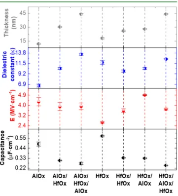
365
because of the higher amount organics to be decomposed;
366
nevertheless, the film degradation is relevant regardless of the
367
film densification.
368
3.3. Dielectric Multilayer Electrical Characterization.
369
The increasing number of high-κ dielectric layers using
370
combustion synthesis and DUV treatment were studied to
371
determine the best dielectric composition and dielectric/
372
semiconductor interface. The electrical characterization of all
373
dielectrics was performed by measuring the capacitance−
374
voltage (C−V), capacitance-frequency (C−f), and breakdown
375
voltage (E) of metal−insulator-semiconductor (MIS)
struc-376
tures, see Figure S6.
377
In order to clarify the dielectrics performance a statistical
378
analysis was done, as depicted inFigure 4andTable S1. Higher
379
dielectric constants for the multilayer dielectrics with three
380
layers, AlOx|HfOx|AlOx (13.5) and HfOx|AlOx|HfOx (12.5)
381
were obtained, as depicted in Figure 4. However, dielectric
382
constant is slightly higher for the AlOx|HfOx|AlOx due to the
383
higher capacitance of the multilayer. In the case of HfOx, the 384
highest dielectric constant was obtained, as expected, but when
385
you add a second layer of HfOx, the dielectric constant
386
decreases because the thin film produced has more residual
387
chloride species. This species will slow down the
dehydrox-388
ylation process and increase the amount of oxygen vacancies in
389
the thin film, which affects the dielectric constant.15 In the
390
other cases, when a layer of HfOx in AlOx is added, the
391
dielectric constant increases because of the higher dielectric
392
constant of HfOx. The breakdown voltage using a single layer 393
of HfOxwas improved from 2.7 MV cm−1to 3.6 MV cm−1with 394
a bilayer due to the thickness increase and interface quality. The
395
highest breakdownfield of 4.9 MV cm−1was achieved for the
396
HfOx|AlOx multilayer, which was also enhanced when
397
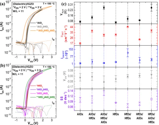
compared with the AlOx|HfOx multilayer, 4.3 MV·cm−1, 398
meaning a better interface when AlOx is in the top of HfOx, 399
as shown in Figure 4. HfOx presents a lower band gap
400
facilitating carrier injection when compared to AlOx. Also, the 401
fact that HfOx precursor contains chlorides leads to increased
402
interface charge defects. Therefore, a higher breakdown voltage
403
is achieved when the AlOxis deposited over HfOx. To further
404
improve the AlOx|HfOx interface quality, a longer annealing 405
could be performed.
406
By increasing the number of layers, the capacitance decrease
407
showing fairly a constant value over the range of frequencies, as
408
presented in Figure S6a.
409
Hysteresis starts to increase in the capacitance−voltage
410
characteristics of the MIS structure, with the increase of the
411
number of layers, as shown inFigure S6b. Theflat band voltage
412
is changed with respect to the different layer composition and
413
increasing the number of layers. The HfOx bilayer shows less 414
hysteresis change when compared with a single layer of HfOx. 415
Taking into account the properties achieved, the most
416
promising dielectrics were all the ones with more than one
417
layer.
418
3.4. Low Voltage Multilayer TFTs. All the TFTs
419
produced at low temperature (150 °C) demonstrated low
420
voltage operation (maximum 3 V) and exhibited a good
421
electrical performance with low gate leakage current. To our
422
knowledge this is thefirst time that TFTs with a single layer of
423
HfOxand multilayers combining AlOxand HfOxsolution based 424
dielectrics are reported at 150 °C. This was possible by the Figure 4. Statistical analysis of capacitance measured at 1 kHz,
dielectric thickness, breakdown voltage, and dielectric constant of all dielectric thinfilms.
DOI:10.1021/acsami.7b11752
ACS Appl. Mater. Interfaces XXXX, XXX, XXX−XXX
425combination of thermal annealing with deep-ultraviolet (DUV) 426irradiation to enhance the intrinsic properties of the films, 427resulting in more uniform and compact films and by using a 428slightly fuel-rich solution combustion synthesis (SCS) which 429decreased the ignition temperature of the exothermic reaction, 430and hence the M-O-M formation. Typical transfer curves of the f5 431TFTs can be observed inFigure 5a, b and the output curves in 432Figure S7. Figure 5b shows that using HfOx layer instead of 433AlOx in contact with the gate electrode facilitates carrier
434injection because of the lower bandgap, resulting in an
435improved interface and lower off current.
436 To study the uniformity and reproducibility of these devices 437a set of 15 devices was produced and characterized for all the 438dielectric thin films, as shown in Figure 5c. This analysis was
439assessed through the measurement of the turn-on voltage
440(VON), hysteresis (VHyst), drain current on−off ratio (ION/IOFF), 441subthreshold slope (SS), and saturation mobility (μSAT), which 442was calculated using the dielectric capacitance measured in MIS 443devices at a frequency of 1 kHz (seeTable S1). High mobility 444that surpassed the state-of-the-art was obtained for all the 445multilayer dielectric TFTs. The highest mobility, 43.9 ± 1.1 446cm2V−1s−1, was achieved for the bilayer of HfOx|HfOx-based 447TFTs. The roughness at the HfOx|AlOx surface may form 448interface charge traps, which increase the carrier scattering 449centers, explaining the lower mobility obtained.16 Other
450reasons for the high carrier mobility achieved for the
451solution-based dielectrics IGZO TFTs are the indium content 452in the IGZO semiconductor and the high areal capacitance of 453the dielectrics used.16In terms of on/off current ratio, most of 454the devices show 1 × 05. We note that a ratio of 1 × 10⁶ is 455achieved for devices with a bilayer of HfOx, which is high when 456compared with literature (Table 1). The turn-on voltage of
457most devices was close to 0. The HfOx|HfOx multilayer
458exhibited less variation of turn-on voltage in different devices. 459The lowest subthreshold slope (SS) value of 0.066 ± 0.01 V
460
dec−1was obtained for (HfOx|HfOx)/IGZO TFTs, indicating 461
the enhanced quality of dielectric-semiconductor interface.
462
All devices showed an anticlockwise hysteresis, as shown in
463 f6
Figure 6a, because of mobile ions, namely some organic
464
residues or defects in the gate dielectric. This is a consequence
465
of using a low temperature (150°C), which can be surpassed
466
by performing a longer annealing time with DUV treatment or
467
using higher temperature.
468
To determine how device performance is affected after aging
469
in air environment, TFTs were again characterized after 2
470
months. The IGZO TFT with the solution-based AlOx|HfOx
471
dielectric showed a slight SS degradation, whereas, the SS of
472
AlOx|HfOx|AlOx multilayer device was larger, as shown in 473
Figure S8 and Table S2. The impact of humidity on the
474
degraded on/off ratio of aged-devices based on the HfOx|AlOx|
475
HfOxmultilayer was also observed .11To improve the quality in 476
the interfaces of layers, longer annealing should be performed
477
and in addition, a device passivation is also suggested.28 All
478
other devices with one and two dielectrics layers showed good
479
stability over time, with only a slight variation of the electrical
480
parameters. The (HfOx|HfOx)/IGZO TFTs revealed the best 481
switching behavior over time, from 0.061 to 0.068 V dec−1, as
482
depicted inFigure 6a.
483
To investigate the devices operational stability, we performed
484
a positive and negative gate bias stress in air environment by
485
applying a constant gate voltage equivalent to electricalfield of
486
±0.5 MV cm−1while keeping the source and drain electrodes 487
grounded. The multilayer devices with 3 layers were not
488
examined due to their instability over time, and also the AlOx 489
single layer did not show an improved performance when
490
compared with literature.11,24The other devices were stressed
491
for 1 h, combined with ∼2 h recovery time in dark condition.
492
Transfer characteristics were obtained in the saturation regime
493
(VDS = 2 V) at selected times during stress and recovery
494
processes, as shown inFigure S9 and S10.Figure 6b shows the Figure 5.(a, b) Typical transfer characteristics of the single and multilayers insulator thinfilms applied in IGZO TFTs; (c) statistical distributions of device parameters, hysteresis (VHyst), saturation mobility (μSAT), current on−off ratio (ION/OFF), turn-on voltage (VON) and subthreshold slope (SS).
DOI:10.1021/acsami.7b11752
ACS Appl. Mater. Interfaces XXXX, XXX, XXX−XXX
495threshold voltage variation (ΔVT) with time during stress and 496recovery phases.
497
By applying a positive gate bias stress (PBS) a maximum VT 498
shift of -0.61 V is obtained for the HfOx|AlOxmultilayer based
499
TFTs. The negative threshold voltage shift under positive gate
500
bias stress of a device employing the AlOx gate dielectric has 501
been reported in a previous publication, where this
502
phenomenon was related to the release of hydrogen from the
503
dielectric to the semiconductor.7
504
The TFTs with AlOx|HfOx multilayer, having the HfOx in 505
contact to the channel show dual shift of threshold voltage (see
506
Figure S8). Simultaneously, two mechanisms contribute for the
507
TFT instability: (i) Negative shift related to the AlOxlayer7and
508
(ii) charge trapping into the dielectric and/or at the interface of
509
channel and dielectric (HfOx) which results in the positive shift
510
of threshold voltage. Interestingly, the electron donating effect
511
happens although the AlOxlayer is not located at the interface 512
to the semiconductor. This means that the hydrogen can easily
513
penetrate into the HfOx layer.
514
The TFTs with HfOx|AlOx in contact to the channel are 515
recovered in 15 min, whereas the ones with AlOx|HfOxare not
516
fully recovered after 3 h of rest in dark condition. The single
517
and bilayers of HfOxapplied in IGZO TFTs were the ones that 518
presented lower positive VT shift under PBS. However, after
519
removing the stress, the threshold voltage is still shifting toward
520
the positive direction even more pronounced than when the
521
TFT is under PBS (seeFigure S9). The recovery of the devices
522
to the initial state can be only achieved by a reannealing process
523
of the TFTs. It is possible that this shows how under PBS
524
compensating acceptor defects are created which persist
525
beyond the stressing. In addition, the residual Cl may be a
526
strong candidate for an extra trap sites in the HfOx layer.15
527
Further investigations are required to elucidate the mechanism
528
at the HfOx/IGZO interface, which leads to the absence of
529
recovery.
530
The VT under negative gate bias stress (NBS) for the
531
different conditions showed a small negative shift with
532
negligible degradation of SS, which is frequently reported for
533
n-type semiconductor TFTs (see more detail Figure S10).40 Figure 6. (a) Aging effect of (HfOx|HfOx)/IGZO TFTs after 2
months; (b) threshold voltage variation (ΔVT) during a 0.5 MV cm−1
stress in selected dielectrics under PBS and NBS tests for 1 h in air environment.
Figure 7.(a) Voltage transfer characteristics and signal gain of the diode-connected inverter with (HfOx|HfOx)/IGZO TFTs. (b) Voltage gain for
different frequencies and (c) a dynamic switching behavior of the inverter under AC square waves at 100 Hz.
DOI:10.1021/acsami.7b11752
ACS Appl. Mater. Interfaces XXXX, XXX, XXX−XXX
534 3.5. Diode-Connected Inverter. Because the (HfOx| 535HfOx)/IGZO thin film transistors revealed the best electrical 536performance, a good stability and uniformity, we applied them 537in a basic building block, an inverter. The structure of this 538circuit was performed using two TFTs, the load and the driver, 539with the same W/L = 11. The load TFT had the gate short-540circuited with the drain in order to work as a resistor. The 541voltage transfer characteristics (VTC) of the obtained inverter 542were measured at various supplied voltages (VDD), 1, 1.5, and 2 f7 543V, as shown in Figure 7a. It is noticed that the output high 544voltage, 1.9 V, is close to the VDD, 2 V, and the output low
545voltage is 0.3 V, when was supposed to be 0 V. For this
546configuration the high output value is VDD− VT (LOAD)and for 547the low output value a higher than 0 V is expected, as the load 548TFT cannot be completely turned OFF. The inverter exhibits a
549maximum gain (−∂VOUT/∂VIN) of 1.15 for the different
550supplied voltages, but due to the use of two identical TFTs 551the expected value was 1. This difference can be explained by a 552slight mismatch between the two TFTs, as depicted inFigure 553S11.
554 To investigate the alternative current (AC) characteristic of
555the inverter, we measured the dynamic behavior under AC
556square wave for different frequencies and the result is shown in 557Figure 7b. The device exhibited good inversion properties, 558however, the gain decreased slightly with the increase of the 559frequency, more precisely to 1 kHz. The gain values are smaller 560in the dynamic measurements when compared with the values 561in the static VTC curve because a buffer was not used to 562provide enough current for full voltage swing, losing some 563current in the cables. To improve the AC results, some tests of 564etching should be done to produce structures suitable for these 565measurements. Figure 7c shows that the device can achieve 566sufficient switching speeds for wearable applications.
4. CONCLUSIONS
567In this work, we have demonstrated for the first time the 568combustion solution synthesis alliance with UV treatment in 569HfOx dielectric thinfilms and multilayer thin films using AlOx
570and HfOx at low temperatures (150 °C) and their
571implementation in electronic structures. The physical proper-572ties of the single layers and multilayers were investigated using a 573wide range of characterization techniques that revealed smooth 574surface (<1.2 nm), high-κ (13.5), high transparency (>89%), 575low leakage currents, and high breakdown voltages (>2.7 MV 576cm−1). The multilayer MIS devices exhibit an improvement by 577presenting low capacitance dependence at low frequencies 578when compared with the single layers. In terms of thin film 579transistors (TFTs), the (HfOx|HfOx)/IGZO TFTs showed the 580best electrical performance with low voltage operation, low 581subthreshold slope (0.066 ± 0.01 V dec−1), 0 V turn-on 582voltage, a high saturation mobility (43.9± 1.1 cm2V−1s−1) and 583current ratio of 1 × 10⁶. This device also presented good 584stability over time (2 months) and under positive gate bias 585stress (PBS) for 1 h, having a maximum threshold voltage 586variation of 0.06 V. These devices were applied in a diode-587connected inverter showing good switching speed at 100 Hz 588with a maximum gain of 1 at 2 V. Taking in consideration the 589excellent results achieved in this report, the next step will be the 590implementation in large-area processing techniques.
591
■
ASSOCIATED CONTENT592
*
S Supporting Information593
The Supporting Information is available free of charge on the
594
ACS Publications websiteat DOI:10.1021/acsami.7b11752.
595
Relevant data related to the production of high-κ
596
dielectric thin films from solution combustion synthesis
597
combined with ultraviolet (UV) treatment and their
598
application in TFTs; Figure S1 and S2 show XRD
599
diffractograms and the FTIR spectra of multilayer
600
dielectric thin films, respectively. Figure S3 depicts
601
AFM surface morphology of multilayer dielectric thin
602
films; Figure S4 show the SEM-FIB cross-section image
603
of multilayer dielectric thin films to determine film
604
thickness; Figure S5 depicts the influence of the fuel in
605
AlOx thin film thickness for different concentrations 606
assisted by UV treatment; Figure S6 show the
607
capacitance−frequency, capacitance−voltage, and current
608
density (J) characteristics of Al/p-type Si/(Dielectric)/Al
609
MIS capacitors with single and multilayer dielectric thin
610
films; Table S1 show the summary of dielectric
611
properties obtained for the capacitors; Figure S7 depicts
612
the typical output curves of all dielectrics conditions
613
applied in TFTs; Figure S8 and Table S2 show the
614
electrical characteristics obtained for the different
615
dielectric conditions applied in IGZO TFTs after 2
616
months in air environment; Figures S9 and S10 show the
617
transfer curves after stress and recovery measurements of
618
the dielectric bilayers applied in IGZO TFTs; Figure S11
619
depicted the transfer curves of TFTs used in the
diode-620 connected inverter (PDF) 621
■
AUTHOR INFORMATION 622 Corresponding Authors 623 *E-mail:elvira.fortunato@fct.unl.pt. 624 *E-mail:ritasba@fct.unl.pt. 625 ORCID 626 Rita Branquinho: 0000-0001-9771-8366 627 Elvira Fortunato: 0000-0002-4202-7047 628 Notes 629The authors declare no competingfinancial interest.
630
■
ACKNOWLEDGMENTS631
This work is funded by FEDER funds through the COMPETE
632
2020 Programme and National Funds through FCT
-633
Portuguese Foundation for Science and Technology under
634
project number POCI-01-0145-FEDER-007688, Reference
635
UID/CTM/50025. European Community H2020
NMP-22-636
2015 project 1D-NEON Grant Agreement 685758. A.K.
637
acknowledges FCT-MEC for a postdoctoral grant (Grant
638
SFRH/BPD/99136/2013). J.M. acknowledges FCT-MEC for a
639
doctoral grant (Grant SFRH/BD/122286/2016). E.C.
ac-640
knowledges FCT-MEC for a doctoral grant (Grant SFRH/
641
BD/116047/2016) and IDS-FunMat-INNO project FPA2016/
642
EIT/EIT RawMaterials Grant Agreement 15015. The authors
643
acknowledge J. V. Pinto and S. Pereira for XRD, D. Nunes for
644
SEM-FIB, and T. Sequeira for AFM measurements.
645
■
REFERENCES(1)Lorenz, M.; Ramachandra Rao, M. S.; Venkatesan, T.; Fortunato, 646 647
E.; Barquinha, P.; Branquinho, R.; Salgueiro, D.; Martins, R.; Carlos,
648
E.; Liu, A.; Shan, F. K.; Grundmann, M.; Boschker, H.; Mukherjee, J.;
DOI:10.1021/acsami.7b11752
ACS Appl. Mater. Interfaces XXXX, XXX, XXX−XXX
649Priyadarshini, M.; DasGupta, N.; Rogers, D. J.; Teherani, F. H.; 650Sandana, E. V.; Bove, P.; Rietwyk, K.; Zaban, A.; Veziridis, A.;
651Weidenkaff, A.; Muralidhar, M.; Murakami, M.; Abel, S.; Fompeyrine,
652J.; Zuniga-Perez, J.; Ramesh, R.; Spaldin, N. A.; Ostanin, S.; Borisov,
653V.; Mertig, I.; Lazenka, V.; Srinivasan, G.; Prellier, W.; Uchida, M.;
654Kawasaki, M.; Pentcheva, R.; Gegenwart, P.; Miletto Granozio, F.; 655Fontcuberta, J.; Pryds, N. The 2016 Oxide Electronic Materials and 656Oxide Interfaces Roadmap. J. Phys. D: Appl. Phys. 2016, 49 (43),
657433001. (2)
658 Fortunato, E.; Barquinha, P.; Martins, R. Oxide Semiconductor
659Thin-Film Transistors: A Review of Recent Advances. Adv. Mater.
6602012, 24 (22), 2945−2986.
(3)
661 Park, S.; Kim, C.-H.; Lee, W.-J.; Sung, S.; Yoon, M.-H. Sol-Gel
662Metal Oxide Dielectrics for All-Solution-Processed Electronics. Mater. 663Sci. Eng., R 2017, 114, 1−22.
(4)
664 Glynn, C.; O’Dwyer, C. Solution Processable Metal Oxide Thin 665Film Deposition and Material Growth for Electronic and Photonic
666Devices. Adv. Mater. Interfaces 2017, 4 (2), 1600610. (5)
667 Nayak, P. K.; Busani, T.; Elamurugu, E.; Barquinha, P.; Martins,
668R.; Hong, Y.; Fortunato, E. Zinc Concentration Dependence Study of
669Solution Processed Amorphous Indium Gallium Zinc Oxide Thin Film
670Transistors Using High-K Dielectric. Appl. Phys. Lett. 2010, 97 (18), 671183504.
(6)
672 Salgueiro, D.; Kiazadeh, A.; Branquinho, R.; Santos, L.;
673Barquinha, P.; Martins, R.; Fortunato, E. Solution Based Zinc Tin
674Oxide TFTs: The Dual Role of the Organic Solvent. J. Phys. D: Appl.
675Phys. 2017, 50 (6), 65106. (7)
676 Lee, W.-J.; Park, W.-T.; Park, S.; Sung, S.; Noh, Y.-Y.; Yoon,
M.-677H. Large-Scale Precise Printing of Ultrathin Sol-Gel Oxide Dielectrics
678for Directly Patterned Solution-Processed Metal Oxide Transistor 679Arrays. Adv. Mater. 2015, 27 (34), 5043−5048.
(8)
680 Kim, Y.-H.; Heo, J.-S.; Kim, T.-H.; Park, S.; Yoon, M.-H.; Kim, J.;
681Oh, M. S.; Yi, G.-R.; Noh, Y.-Y.; Park, S. K. Flexible Metal-Oxide
682Devices Made by Room-Temperature Photochemical Activation of
683Sol−gel Films. Nature 2012, 489 (7414), 128−132.
(9)
684 Kim, M.-G.; Kanatzidis, M. G.; Facchetti, A.; Marks, T. J.
Low-685Temperature Fabrication of High-Performance Metal Oxide Thin-Film
686Electronics via Combustion Processing. Nat. Mater. 2011, 10 (5), 687382−388.
(10)
688 Park, S.; Kim, K. H.; Jo, J. W.; Sung, S.; Kim, K. T.; Lee, W. J.;
689Kim, J.; Kim, H. J.; Yi, G. R.; Kim, Y. H.; Yoon, M. H.; Park, S. K.
In-690Depth Studies on Rapid Photochemical Activation of Various Sol-Gel
691Metal Oxide Films for Flexible Transparent Electronics. Adv. Funct.
692Mater. 2015, 25 (19), 2807−2815. (11)
693 Carlos, E.; Branquinho, R.; Kiazadeh, A.; Barquinha, P.; Martins, 694R.; Fortunato, E. UV-Mediated Photochemical Treatment for Low-695Temperature Oxide-Based Thin-Film Transistors. ACS Appl. Mater.
696Interfaces 2016, 8 (45), 31100−31108.
(12)
697 Dey, A.; Kalita, A.; Iyer, P. K. High-Performance N - Channel
698Organic Thin-Film Transistor Based on Naphthalene Diimide. ACS
699Appl. Mater. Interfaces 2014, 6, 12295−12301. (13)
700 Kim, S. J.; Jang, M.; Yang, H. Y.; Cho, J.; Lim, H. S.; Yang, H.;
701Lim, J. A. Instantaneous Pulsed-Light Cross-Linking of a Polymer Gate 702Dielectric for Flexible Organic Thin-Film Transistors. ACS Appl. 703Mater. Interfaces 2017, 9 (13), 11721−11731.
(14)
704 Li, Y.; Lan, L.; Xiao, P.; Sun, S.; Lin, Z.; Song, W.; Song, E.;
705Gao, P.; Wu, W.; Peng, J. Coffee-Ring Defined Short Channels for
706Inkjet-Printed Metal Oxide Thin-Film Transistors. ACS Appl. Mater.
707Interfaces 2016, 8 (30), 19643−19648. (15)
708 Liu, A.; Guo, Z.; Liu, G.; Zhu, C.; Zhu, H.; Shin, B.; Fortunato,
709E.; Martins, R.; Shan, F. Redox Chloride Elimination Reaction: Facile 710Solution Route for Indium-Free, Low-Voltage, and High-Performance
711Transistors. Adv. Electron. Mater. 2017, 3, 1600513. (16)
712 Zhang, F.; Liu, G.; Liu, A.; Shin, B.; Shan, F. Solution-Processed
713Hafnium Oxide Dielectric Thin Films for Thin-Film Transistors
714Applications. Ceram. Int. 2015, 41 (10), 13218−13223.
(17)
715 Kim, Y. G.; Avis, C.; Jang, J. Low Voltage Driven, Stable
716Solution-Processed Zinc-Tin-Oxide TFT with HfOy and AlOx Stack
717Gate Dielectric. ECS Solid State Lett. 2012, 1 (2), Q23−Q25.
(18)Park, J. H.; Lee, S. J.; Lee, T. I.; Kim, J. H.; Kim, C.-H.; Chae, G. 718 719
S.; Ham, M.-H.; Baik, H. K.; Myoung, J.-M. All-Solution-Processed,
720
Transparent Thin-Film Transistors Based on Metal Oxides and
Single-721
Walled Carbon Nanotubes. J. Mater. Chem. C 2013, 1 (9), 1840−1845. (19)Branquinho, R.; Salgueiro, D.; Santos, L.; Barquinha, P.; Pereira, 722
723
L.; Martins, R.; Fortunato, E. Aqueous Combustion Synthesis of
724
Aluminum Oxide Thin Films and Application as Gate Dielectric in
725
GZTO Solution-Based TFTs. ACS Appl. Mater. Interfaces 2014, 6 (22),
726
19592−19599.
(20)Han, S. W.; Park, J. H.; Yoo, Y. B.; Lee, K. H.; Kim, K. H.; Baik, 727 728
H. K. Solution-Processed Laminated ZrO2/Al2O3 Dielectric for
Low-729
Voltage Indium Zinc Oxide Thin-Film Transistors. J. Sol-Gel Sci.
730
Technol. 2017, 81 (2), 570−575.
(21)Liu, A.; Liu, G. X.; Zhu, H. H.; Xu, F.; Fortunato, E.; Martins, 731 732
R.; Shan, F. K. Fully Solution-Processed Low-Voltage Aqueous In2O3
733
Thin-Film Transistors Using an Ultrathin ZrOx Dielectric. ACS Appl.
734
Mater. Interfaces 2014, 6 (20), 17364−17369.
(22)Pereira, L.; Barquinha, P.; Fortunato, E.; Martins, R. Influence of 735 736
the Oxygen/argon Ratio on the Properties of Sputtered Hafnium
737
Oxide. Mater. Sci. Eng., B 2005, 118 (1−3), 210−213.
(23)Wang, H.; Sun, T.; Xu, W.; Xie, F.; Ye, L.; Xiao, Y.; Wang, Y.; 738 739
Chen, J.; Xu, J. Low-Temperature Facile Solution-Processed Gate
740
Dielectric for Combustion Derived Oxide Thin Film Transistors. RSC
741
Adv. 2014, 4 (97), 54729−54739.
(24)Park, S.; Kim, K.-H.; Jo, J.-W.; Sung, S.; Kim, K.-T.; Lee, W.-J.; 742 743
Kim, J.; Kim, H. J.; Yi, G.-R.; Kim, Y.-H.; Yoon, M.-H.; Park, S. K.
In-744
Depth Studies on Rapid Photochemical Activation of Various Sol-Gel
745
Metal Oxide Films for Flexible Transparent Electronics. Adv. Funct.
746
Mater. 2015, 25 (19), 2807−2815.
(25)Avis, C.; Kim, Y. G.; Jang, J. Solution Processed Hafnium Oxide 747 748
as a Gate Insulator for Low-Voltage Oxide Thin-Film Transistors. J.
749
Mater. Chem. 2012, 22 (34), 17415.
(26)Gao, Y. N.; Xu, Y. L.; Lu, J. G.; Zhang, J. H.; Li, X. F. Solution750 751
Processable Amorphous Hafnium Silicate Dielectrics and Their
752
Application in Oxide Thin Film Transistors. J. Mater. Chem. C 2015,
753
3 (43), 11497−11504.
(27) Esro, M.; Vourlias, G.; Somerton, C.; Milne, W. I.; 754 755
Adamopoulos, G. High-Mobility ZnO Thin Film Transistors Based
756
on Solution-Processed Hafnium Oxide Gate Dielectrics. Adv. Funct.
757
Mater. 2015, 25 (1), 134−141.
(28)Kiazadeh, A.; Gomes, H. L.; Barquinha, P.; Martins, J.; Rovisco, 758 759
A.; Pinto, J. V.; Martins, R.; Fortunato, E. Improving Positive and
760
Negative Bias Illumination Stress Stability in Parylene Passivated
761
IGZO Transistors. Appl. Phys. Lett. 2016, 109 (5), 051606.
(29)Weng, J.; Chen, W.; Xia, W.; Zhang, J.; Jiang, Y.; Zhu, G. Low-762 763
Temperature Solution-Based Fabrication of High-K HfO2 Dielectric
764
Thin Films via Combustion Process. J. Sol-Gel Sci. Technol. 2017, 81,
765
662−668.
(30)González-Cortés, S. L.; Imbert, F. E. Fundamentals, Properties 766 767
and Applications of Solid Catalysts Prepared by Solution Combustion
768
Synthesis (SCS). Appl. Catal., A 2013, 452, 117−131.
(31) González-Cortés, S. L.; Imbert, F. E. Advanced Synthesis of769 770
Materials for Intermediate-Temperature Solid Oxide Fuel Cells. Appl.
771
Catal., A 2013, 452 (4), 117−131.
(32)González-Cortés, S. L.; Imbert, F. E. Fundamentals, Properties 772 773
and Applications of Solid Catalysts Prepared by Solution Combustion
774
Synthesis (SCS). Appl. Catal., A 2013, 452, 117−131.
(33)Jain, S. R.; Adiga, K. C.; Pai Verneker, V. R. A New Approach to 775 776
Thermochemical Calculations of Condensed Fuel-Oxidizer Mixtures.
777
Combust. Flame 1981, 40, 71−79.
(34) Branquinho, R.; Salgueiro, D.; Santa, A.; Kiazadeh, A.; 778 779
Barquinha, P.; Pereira, L.; Martins, R.; Fortunato, E. Towards
780
Environmental Friendly Solution-Based ZTO/AlO X TFTs. Semicond.
781
Sci. Technol. 2015, 30 (2), 024007.
(35)Epifani, M.; Melissano, E.; Pace, G.; Schioppa, M. Precursors for 782 783
the Combustion Synthesis of Metal Oxides from the Sol−gel
784
Processing of Metal Complexes. J. Eur. Ceram. Soc. 2007, 27 (1),
785
115−123.
DOI:10.1021/acsami.7b11752
ACS Appl. Mater. Interfaces XXXX, XXX, XXX−XXX
(36)
786 Faber, H.; Lin, Y.; Thomas, S. R.; Zhao, K.; Pliatsikas, N.;
787McLachlan, M. A.; Amassian, A.; Patsalas, P. A.; Anthopoulos, T. D. 788Indium Oxide Thin-Film Transistors Processed at Low Temperature
789via Ultrasonic Spray Pyrolysis. ACS Appl. Mater. Interfaces 2015, 7 (1), 790782−790.
(37)
791 Neumayer, D. A.; Cartier, E. Materials Characterization of
792ZrO2−SiO2 and HfO2−SiO2 Binary Oxides Deposited by Chemical 793Solution Deposition. J. Appl. Phys. 2001, 90 (4), 1801−1808.
(38)
794 Toledano-Luque, M.; San Andrés, E.; Olea, J.; del Prado, A.; 795Mártil, I.; Bohne, W.; Röhrich, J.; Strub, E. Hafnium Oxide Thin Films 796Deposited by High Pressure Reactive Sputtering in Atmosphere
797Formed with Different Ar/O2 Ratios. Mater. Sci. Semicond. Process. 7982006, 9 (6), 1020−1024.
(39)
799 Reyes, J. M.; Perez Ramos, B. M.; Islas, C. Z.; Arriaga, W. C.;
800Quintero, P. R.; Jacome, a. T. Chemical and Morphological 801Characteristics of ALD Al2O3 Thin-Film Surfaces after Immersion
802in pH Buffer Solutions. J. Electrochem. Soc. 2013, 160 (10), B201− 803B206.
(40)
804 Chang, Y.-H.; Yu, M.-J.; Lin, R.-P.; Hsu, C.-P.; Hou, T.-H.
805Abnormal Positive Bias Stress Instability of In−Ga−Zn−O Thin-Film 806Transistors with Low-Temperature Al2O3 Gate Dielectric. Appl. Phys.
807Lett. 2016, 108 (3), 033502.
DOI:10.1021/acsami.7b11752
ACS Appl. Mater. Interfaces XXXX, XXX, XXX−XXX