F
ACULDADE DEE
NGENHARIA DAU
NIVERSIDADE DOP
ORTOEducational package based on the
MIPS architecture for FPGA platforms
João Luís Silva Campos Pereira
Thesis submitted under the course of:
Integrated Master In Electrical and Computer Engineering Major in Telecomunications
Tutor: Professor José Carlos dos Santos Alves
c
Resumo
O paradigma do ensino tem vindo a evoluir como resultado da constante evolução tecnológica. As recentes evoluções, tanto na implementação de tecnologias digitais como na tecnologia de informação tornam possível um processo de aprendizagem mais activo por parte dos estudantes. Além disso, o acesso ao conhecimento é na sua maioria suportado por sistemas computacionais capazes de processar grandes quantidades de informação. Esta competência requer, entre outros componentes, processadores de elevado desempenho.
A arquitectura MIPS 32bit teve origem no trabalho realizado por uma equipa liderada por John Hennessy, tornando-se em 1984 numa arquitectura pioneira de CPUS de tipo RISC. Jun-tamente com o seu sucesso no mercado embutido, a arquitectura MIPS 32bit tem vindo a ser largamente utilizada como caso de estudo em Arquitecturas de Computadores por todo o mundo. Nesta dissertação a arquitectura MIPS 32bit foi estudada de modo a que os processares pudessem ser correctamente implementados.
Alguns trabalhos anteriormente existentes já incluem simuladores de processadores MIPS e até implementações de processadores MIPS baseadas em hardware. No entanto, este trabalho refere-se ao desenvolvimento de uma implementação fiel das três versões de processadores ref-erenciadas em “Computer Organization and Design - the hardware/software interface”, de John Hennessy e David Patterson, com o intuito de implementar exactamente as mesmas funcionali-dades referenciadas no livro. O projecto visou a implementação na Spartan3 XC3S200 presente num kit de desenvolvimento de baixo custo frequentemente usado em fins didácticos em gradu-ações em Engenharia Electrotécnica e de Computadores.
O trabalho desenvolvido compreende ambos os processadores de um ciclo por instrução e de mais de um ciclo por instrução, assim como, uma versão pipeline com mecanismos que evitem irregularidades na execução. Estes processadores foram integrados com módulos de controlo adi-cionais, incluindo contadores de eventos realizados, e com a interface desenvolvida em software para interagir com os referidos processadores.
Abstract
The teaching paradigm has been evolving as a result of the constant technological developments. Recent developments, either in the digital implementation technologies and in information tech-nology make possible a more active learning process by the students. Furthermore, the access to knowledge is mainly supported by computer systems, capable of processing large amounts of information. This competence requires, among other components, high performance processors.
The MIPS 32bit architecture started with the work performed by a team led by John Hennessy and thus became a pioneer in RISC CPUs in 1984. Along with its success in the embedded market, MIPS 32bit is being widely used as a case of study in computer architectures around the world. In this dissertation, the MIPS 32bit architecture was studied so the processors could be properly implemented.
Some previously existent works already comprise MIPS processors simulators and even MIPS based processors implementations in hardware. However, this work addresses the development of a truthful implementation of the three processors versions referenced in “Computer Organization and Design - the hardware/software interface”, of John Hennessy and David Patterson, to imple-ment exactly the same functionalities addressed in the reference text book. The project targeted the Spartan3 XC3S200 which is a low-cost development kit commonly used for teaching purposes in Electrical and Computer Engineering graduations.
The developed work comprehends both single clock and multi clock cycle per instruction processor, as well as, a pipeline version with hazard evading mechanisms. These processors were integrated with additional control modules, including performed event counters, and the software interface developed to interact with the referred processors.
Acknowledgments
This thesis was the consummation of a rich learning period. There were many people who pos-itively contributed to this thesis achievement. To these people I want to thank you for your con-tribution either in a more technical level inherent to the project development, or in a second stage level providing the proper support.
Therefore, I start by thanking to my family, to my Father, Mother and Brother for encouraging me and for all the economic effort and affective support provided through my entire life.
A very special thank you goes out to my dear Vanessa for the given motivation and support. She patiently tolerated the absence of my person during the project development as well as during the thesis writing when I retreated to long days with my computer.
I would like to express my gratitude to my tutor, Professor José Carlos Alves for the devoted time to my project along with all the recommendations and provided directions towards the project development.
A word of appreciation to Professor João Canas Ferreira is legitimately expressed to acknowl-edge the enduring suggestions towards the inclusion of features to the developed system.
The burden of writing this thesis was substantially mitigated by the support and humor of my lab mates; Alfredo Moreira, Carlos Resende, João Rodrigues, João Santos, Nuno Pinto and Pedro Santos. Thank you for your recommendations and good company.
I would also like to thank to my “brother in arms” Renato Caldas for the suggestions, and for the enthusiasm shown during the project realization.
Finally, I would like to thank to Tim Parys from the University of Rhode Island and to Se-bastian Kuligowski respectively for the Configurable Assembler and the Java serial Port drivers which undoubtedly spared considerable time.
To each of the above mentioned, I extend my deepest appreciation.
João Luís Silva Campos Pereira
“The major difference between a thing that might go wrong and a thing that cannot possibly go wrong is that when a thing that cannot possibly go wrong goes wrong, it usually turns out to be impossible to get at and repair.”
Douglas Adams
Contents
1 Introduction 1 1.1 Motivation . . . 2 1.2 Objectives . . . 2 1.3 Work summary . . . 2 1.4 Document Overview . . . 3 2 Background 5 2.1 Relevant Literature . . . 52.2 Computer Architectures used for Teaching . . . 6
2.2.1 MIPS 32bit Architecture . . . 6
2.2.2 DLX Architecture . . . 9 2.3 Hardware Platform . . . 9 2.3.1 Spartan 3 . . . 10 2.4 Software Platform . . . 11 2.4.1 JAVA . . . 11 2.4.2 Eclipse . . . 12 2.5 Related Projects . . . 12 2.6 Concluding Remarks . . . 15 3 System Specifications 17 3.1 Development Methodology . . . 17 3.1.1 The Hardware . . . 17 3.1.2 Software . . . 19
3.2 System Abstraction Model . . . 19
3.3 MIPS Instruction Set . . . 20
3.4 Implemented Processor Models . . . 22
3.4.1 Unicycle . . . 23
3.4.2 Multicycle . . . 26
3.4.3 Pipelined . . . 30
3.5 Event Counters . . . 36
3.6 Concluding Remarks . . . 37
4 Implementation and Results 39 4.1 Hardware . . . 39
4.1.1 Serial Manager . . . 40
4.1.2 Memory . . . 41
4.1.3 The Register File . . . 44
4.1.4 Program Counter . . . 44 ix
x CONTENTS
4.1.5 The Control Manager . . . 44
4.1.6 The Unicycle processor . . . 47
4.1.7 The Multicycle processor . . . 49
4.1.8 The Pipelined version processor . . . 51
4.1.9 Event Counters . . . 56
4.1.10 Performance evaluation . . . 57
4.1.11 Implementation with 32bit counters . . . 58
4.2 Software . . . 60
4.2.1 JAVA Graphic User Interface . . . 60
4.2.2 MIPS Language Assembler . . . 62
4.3 Concluding Remarks . . . 62
5 Conclusions and Future Work 65 5.1 Objectives Accomplishment . . . 65
5.2 Future Work . . . 66
A Figures 67
List of Figures
2.1 MIPS Set extensions, based in [1]. . . 7
2.2 Byte addressable Memory, based in [2]. . . 8
2.3 Spartan-3 Family Architecture. [3]. . . 10
2.4 JVM and JIT Compiler [4] . . . 12
3.1 System Abstraction Model. . . 20
3.2 Unicycle, based in [2]. . . 23
3.3 Multicycle, based in [2]. . . 28
3.4 Multicycle FSM. . . 31
3.5 Pipeline versus Unicycle. . . 32
3.6 Pipeline basic design, based in [2]. . . 33
3.7 Control signals transition in pipeline, based in [2]. . . 34
3.8 Pipeline version with forwarding mechanisms, based in [2] . . . 35
4.1 Serial Manager operation example. . . 40
4.2 Finite State Machine of the Serial Manager block. The comments in italic refer to state transition conditions. . . 41
4.3 Command execution of the Instruction Memory write command. The values of “counter” refer to each command execution state and the comments in italic refer to state transition conditions. . . 42
4.4 Command execution of the read of the Instructions Type counter. The values of “counter” refer to each command execution state and the comments in italic refer to state transition conditions. . . 43
4.5 Register file and associated multiplexers. . . 45
4.6 Register file wrapper which includes the contents of figure4.5. . . 45
4.7 Control Manager ports. . . 46
4.8 Control Manager finite state machine. . . 46
4.9 Control Manager auxiliary states. . . 47
4.10 Unicycle control signals during the execution of two instructions. . . 48
4.11 Muticycle control signals. . . 50
4.12 Pipeline control signals, A. . . 52
4.13 Pipeline control signals, B. . . 53
4.14 Pipeline hazard avoiding mechanisms, based in [2]. . . 55
4.15 Setup Interface. . . 61
4.16 Unicycle interface. . . 62
A.1 Serial Manager. . . 68
A.2 Unicycle interface. . . 69
A.3 Multicycle interface. . . 70 xi
xii LIST OF FIGURES
List of Tables
3.1 R-Type Instruction, [2]. . . 21
3.2 I-Type Instruction, [2]. . . 21
3.3 Jump Instruction, [2]. . . 21
3.4 Adopted Instruction Set. X stands for “don’t care”, n.a. stands for not applicable. Based in MIPS Instruction Set [2] . . . 22
3.5 Control Unit table. x stands for “dont’t care”. Based in [2] . . . 24
3.6 ALU Control table. X stands for “don’t care”. Based in [2] . . . 25
3.7 Instructions length, based in [2]. . . 26
4.1 Unicycle processor used resources and maximum frequency . . . 48
4.2 Multicycle processor used resources and maximum frequency, post place and route. 51 4.3 Pipeline processor used resources and maximum frequency, post synthesis. . . . 54
4.4 Pipeline processor used resources and maximum frequency post place and route. 56 4.5 Processors frequency. . . 57
4.6 Processors performance case of study. . . 58
4.7 Unicycle processor used resources and maximum frequency with 32bit counters (XC3S400). . . 58
4.8 Multicycle processor used resources and maximum frequency with 32bit counters (XC3S400). . . 59
4.9 Pipeline processor used resources and maximum frequency with 32bit counters (XC3S400). . . 59
Abbreviations
ARM Advanced RISC MachineCISC Complex Instruction Set Computer COD Computer Organization Design CPI Clocks per Instruction
CPU Central Processing Unit DVD Digital Video Disc
FEUP Faculdade de Engenharia da Universidade do Porto GUI Graphical User Interface
HD DVD High Density Digital Video Disc I-Type Immediate Instruction Format IP Intelectual Property
MIPS Microprocessor without Interlocked Pipeline Stages FPGA Field Programmable Gate Array
RISC Reduced Instruction Set Computer R-Type Register-Register Instruction Format SoC System on Chip
SPARC Scalable Processor ARChitecture
Chapter 1
Introduction
The computer has become an essential tool in the support of the modern teaching methods, man-aging knowledge at a time when the information is expanding exponentially. The increasingly computation needs among Personal Computers, Servers and Embedded systems demand for more capacity in matter of program execution speed. The computer architecture is a key factor in the computer performance and is subject of study in many universities over the world.
Computer architecture is a major subject in current Electrical and Computer Engineering grad-uations in its importance in providing to the students the know-how of the processors operation and processor design. In such a technical field of study, the hands-on experience is considered to be a fundamental pedagogic technique for motivating students to understand new topics. Furthermore, learning the hardware organization and the physical limitations associated to the implementation of real processors can help students to understand the hardware foundations of modern computers and consequently foster the development of new processing systems.
Among the existent computer architectures, the 32bits MIPS is considered the architecture of choice for didactic purpose by the prestigious Universities around the world in this field of study. The MIPS 32bit was a pioneer in the CPUs RISC development, being nowadays present in many consumer electronics and embedded systems.
This thesis addresses the computer architecture book “Computer Organization and Design - the hardware/software interface”, of John Hennessy and David Patterson, which is a work of reference on Computer Architectures also used in many universities worldwide [2].
Aiming at educational purposes, the scope of this work is to develop hardware implemented processors targeting low complicity and low cost FPGA boards, which are of common use in Universities for practicing digital design. This is an open source design that the students may freely modify in order to add new functionalities or adapt to their requirements.
2 Introduction
1.1
Motivation
The tendency nowadays in the training of the engineers is to make use of recent technologies for better understanding and consolidation of knowledge [5]. The previous observation combined with the importance of computer processor advances in modern society bears the aim of this work. It consists in creating an educational package to support the teaching of Computer Architectures introductory courses as a complement to the previously referenced book. This way, students can improve and extend their knowledge in computer architecture and, at the same time, develop skills and acquire experience on the draft of digital reconfigurable systems (FPGAs). The chosen architecture is MIPS 32bit whose CPUs formed the basis of embedded Processors field since the 1980s until now. To overcome this, the work proposes the development of a set of processors that follow the models addressed in the referenced text book.
1.2
Objectives
Taking out the motivation that led to this work, the general objective was defined as to develop a low-cost educational package targetable to low-cost FPGA boards. This package consisted of processors models studied in the book previously referred, as well as, software tools and their documentation. More detailed objectives are set as:
• develop a single clock cycle per instruction Processor, a multi clock cycle per instruction Processor and a Pipelined Processor version, all in hardware1;
• develop a Computer-FPGA interface capable of control the processor’s clock and provide random access to registers and memory;
• develop counters to monitor performed events, such as number of clocks, executed instruc-tions types, data accesses and memory accesses;
• develop a JAVA Software Graphic User Interface to interact with the FPGA; • develop a MIPS language assembler;
• develop a support for a Cache Memory;
• writing of the thesis and all the manuals in English;
1.3
Work summary
The developed work includes the integration of two different systems towards the conception of simple and easy to understand processor models. The three proposed processor versions were
1from now on, the single clock cycle per instruction Processor, as well as, the multi clock cycle per instruction
1.4 Document Overview 3
successfully implemented and comprehend a basic MIPS instruction set. The third processor version complies pipeline hazards resolution techniques, which can be optionally enabled from the interface. As a complement to the processors design, the events performed during the processor runtime can be identified and enumerated. An instruction set dedicated assembler was created in order to spare the tedious and manual assembly language translation, into processor recognizable operational codes. The user interaction with the processors is assured by a Java based graphic user interface, providing total access to both processors and counters inherent storage elements, as well as, to the processors operational modes.
1.4
Document Overview
This work describes the development of hardware Processors implemented in a FPGA board, as well as, the development of the Processors correspondent software interface. This Dissertation is composed of five chapters. In Chapter2, the MIPS 32bit Architecture, as well as, the referenced Book are reviewed and discussed. In the same chapter are specified both hardware and software platforms, respectively the FPGA used for the project and the software development tool. In the end of the very same chapter, relevant related projects will be addressed. Chapter 3 shows the methodology employed to develop the modules, the used Instruction Language and the specifica-tion of the developed modules. Chapter4describes the performed implementation and presents the results obtained. In Chapter5a review is made about the accomplished objectives and suggestions for improvement are presented.
Chapter 2
Background
This chapter presents the literature considered relevant for this work, the development of the MIPS architecture and discusses the main tools used to carry out the work performed. At the end of the chapter, similar educational projects are addressed.
2.1
Relevant Literature
The most important Literature obviously is the referenced book "Computer Organization and De-sign - the hardware/software interface", of John Hennessy and David Patterson [2]. Some other books such as "Computer Architecture and Organization", of John P. Hayes [6] or "Computer Ar-chitecture - concepts and evolution", of Gerrit A. Blaauw and Frederick P. Brooks, Jr. [7] can be read for complementary perspectives.
Throughout the book, the author follows two approaches. A more theoretically oriented for the readers whose only purpose is to understand the Processor information flow and another one more technical and detailed approach for those with higher ambitions, like understanding the pro-cessors hardware details. As it will be seen, some programming methods can be improved by understanding all the processes taken place in the processor operation. Not all the MIPS opera-tions are described in the reference text book, however, suggesopera-tions presented by the Author were used in order to implement some of them. The most relevant reading chapters are the second, the third and the fourth chapters which address the computer language, both Unicycle and Multicycle processors and the Pipelining implementation technique.
For a better historical evolution survey the reader can consult “See MIPS Run”, of Dominic Sweetman [1], and in order to take note of related projects in this field of study the reader can also consult “Arquitectura de computadores - dos Sistemas Digitais aos Microprocessadores”, of Guil-herme Arroz, José Monteiro and Arlindo Oliveira [8], as well as “Arquitectura de computadores”, of José Delgado and Carlos Ribeiro [9].
6 Background
2.2
Computer Architectures used for Teaching
Nowadays, there are a few Computer Architectures used in Didactic environments. If a web search is performed, the most common ones are 32bit MIPS, 16bit Motorola 68K and the mobile devices architecture leader, 32bit Arm. Well known reference teaching institutions, such as the Carnegie Mellon University, the University of California in Santa Barbara, the University of California in Berkeley and the Massachusetts Institute of Technology adopt the use of MIPS Architecture, with the referenced COD (Computer Organization and design)text book when concerning the lecture of computer architectures courses, it was considered the most useful and appropriate for this work. Therefore, in this section it will be approached the 32bit MIPS Architecture and a similar one (DLX) whose purpose is not commercial, like in MIPS case, but didactic.
2.2.1 MIPS 32bit Architecture
In 1984, MIPS Computer Systems was founded becoming a pioneer in the CPUs RISC develop-ment. It developed one of the first commercial RISC (Reduced Instruction Set Computer) micro-processors whose properties included small and highly-optimized instructions rather than more complex instructions as in CISC (Complex Instruction Set Computer). RISC processors have a CPI (clock per instruction) of one cycle and usually incorporate a larger number of registers to prevent large amounts of interactions with memory [1]. The company was purchased buy Silicon Graphics, Inc. in 1992, and was spun off as MIPS Technologies Inc. in 1998. MIPS Tech-nologies, Inc. is the world’s second largest semiconductor design IP worldwide company with more than 250 customers around the globe [10], with 100 M MIPS CPUs shipped in 2004 into embedded applications. Today, MIPS powers many consumer electronics and MIPS designs are used in SGI’s (Silicon Graphics Incorporated) computer product line, founding broad application in embedded systems including digital television, broadband access, cable set-top boxes, DVD recorders, HD DVDs and VoIP. Windows CE devices, Cisco routers, the Nintendo 64 console, the Sony PlayStation 2 console, and the Sony PSP handheld system use MIPS processors. The MIPS cores scalability, performance and low power consumption meet the increasing demand for sophis-ticated digital devices. The architecture is similar to that of other recent CPU designs, including Sun’s SPARC, IBM and Motorola’s PowerPC, and ARM-based processors [11].
The MIPS Architecture has evolved through the years of existence as a compromise between program demanding and hardware resources. From the MIPS I, in 1985, to the modern MIPS 32/64 architecture, some remarkable improvements concerning the registers width and numbers representation took place. Since the instructions set extensions were inclusive, each new architec-ture version included the former levels, meaning that a processor can run binary programs from previously implemented instruction sets [1]. Illustrated in figure2.1.
The MIPS I instruction set comprehended the simplest and basic instructions to what would become a well performed and important RISC architecture. Some of those instructions are present in the instruction set used in this work. The MIPS I processors shipped to market were the R2000 and the R3000. The R3000 took the advantage of a more advanced manufacturing process along
2.2 Computer Architectures used for Teaching 7
Figure 2.1: MIPS Set extensions, based in [1].
with some well-judged hardware enhancements, giving a substantial improvement in execution speed. Some pioneers embedded applications such as high-performance laser printers and type-setting equipment used R3000. The second set (MIPS II) added load linked, store conditional and branch likely instructions. Although it has not passed beyond the preproduction is the clos-est set to the modern MIPS32. A couple years later, in 1990, to fulfill the programs growth and consequently longer registers necessity, MIPS became the first 64 bit RISC architecture to reach production with the R4000 processor. That was the MIPS III era. The two following instruction sets (MIPS IV and MIPS V) respectively added the floating point units and the Single Instruction, Multiple Data parallelism technique (SIMD). While the MIPS IV was implemented in two new processors (the R10000 and the R50000), the MIPS V just represented improvements to the previ-ous sets, being present nowadays in MIPS64. Presently, the MIPS32 and MIPS64 are respectively supersets of MIPS II and MIPS IV.
MIPS uses both 32bit and 64 bit architecture but our concern to this work will be only the 32bit, which comprehends 32 registers, each 32 bits wide (a bit pattern of this size is referred to as a word). This way the register addresses are 5 bits long and the data inputs and outputs are 32-bits wide. More than 32 registers might seem better, however, more registers mean more decoders and multiplexers to select individual registers making the design more expensive than using ram, which is cheaper and denser than registers. Nevertheless the registers should be used as much as possible for the simple reason they are faster than ram. Nowadays most compilers can wisely use registers and minimizing ram accesses but in the past using registers intelligently was a programmer concern [2].
It was previously stated that the registers should be used as much as possible, meaning that sometimes the use of ram is inevitably. Arithmetic operations occur only on registers, however, to have data on registers, data transfer instructions must occur. Data transfers occur very often when the computer has to represent complex data structures, such as arrays and structures. The data transfer instruction that copies from the ram to the registers is called Load (LW as Load Word),
8 Background
while the data transfer in the opposite way, from registers to ram, is called Store (SW as Store Word). Loads and stores use indexed addressing to access ram because, and here comes another important architecture property, the memories are byte-addressable. This means that each memory address is 8 bit referenced, which combined with the 32 address lines result in a 4 Gbyte address space. Therefore, given that a 32 bit word can be occupied by 4 bytes each word must start at address multiple of 4 (0, 4, 8, 12, ....) also called alignment restriction.
Figure 2.2: Byte addressable Memory, based in [2]. An example of a MIPS instruction can be:
add $s0, $t0, $t1 ,
where the instruction “tells” the processor to compute the sum of the values in registers $t0 and $t1 and store the result in register $s0. In section3.3 the Instruction Language will be described in more detail [12].
As it was referenced in the previous chapter the basic concept in the development of the MIPS Architecture was to dramatically increase performance with less die area through the use of pipelining technique. Pipelining consists in partially overlap instructions in order to increase performance by "breaking" the instructions process in a series of stages linked between them. Each stage performs a small part of the overall instruction processing while the instruction flows through the datapath. The stages should be perfectly balanced so that each stage takes approxi-mately the same time. The reason for this, concerns the fact that the machine clock cycle is defined by the longest stage execution time. The pipelining paradox is that, for each instruction, the time since the start of the first step until the last one is complete is not shorter than a non-pipelining approach, but when executing several instructions continuously the performance increases so that for the same amount of time the pipelined version surpasses the non-pipelined. The high perfor-mance is achieved by parallel processing of multiple instructions at the same time, each in different stages of the pipeline. It is therefore a key processing technique which was introduced in the RISC architectures, being later adopted by CISC architectures [2], [13], [1]. There are, however, some limitations concerning pipelining instruction execution called hazards, which can be grouped in three different types. The Structural Hazards concern the hardware flaw in supporting the combi-nation of instructions, set to execute in same clock cycle. The Data Hazards, which occur when an
2.3 Hardware Platform 9
instruction cannot be executed in the right clock cycle due to the needed data not being available at that time. Some forwarding techniques can be implemented, as we will see in sub-section3.4.3, to avoid these kind of situations, still, some cases are inevitable. Finally, Control Hazards refer to the issue of the instruction not being executed in the appropriate clock cycle, due to the fact the fetched instruction is not the needed one [2].
2.2.2 DLX Architecture
DLX Architecture is a generic open source 32bit RISC architecture oriented for didactic purpose. In DLX, the complex instructions are simulated in software, by the use of the simple instructions performed by the architecture. It is very similar to MIPS architecture with some evident influ-ences from competing architectures such as DEC VAX, IBM /370 and Intel 8086. Like MIPS, DLX bases its performance on the use of an instruction pipeline and supports the same 3 in-structions types (R-Type, I-Type and Jump), yet with some differences in the instruction fields organization. While in the MIPS Instruction Set, the shift amount is set by a reserved 6 bit field called shamt, in the DLX Instruction Set there is no shift amount field, and the function field is 11bit wide. This difference allows DLX Set to perform dynamic shift operations, meaning that the amount of shifts can be provided not only by a constant but also by a register value. The differ-ence present in the I-Type Instructions is defined by the feature of the DLX Set to allow the load destination register (1) type as unsigned byte, float or double. Both architectures provide byte, half word and word memory loads/stores. The Jump instruction specification is the same as in MIPS Instruction Set since, both architectures allow linked and not-linked jumps (2), as well as the two types of jump destination address. The program counter relative address and the register content address [14], [15].
2.3
Hardware Platform
The FPGAs are integrated circuits consisting of configurable logic blocks (CLBs), I/O pads, and routing channels. These routing channels consist of reconfigurable interconnections, which can be local connections, like links between CLBs neighbors, or global connections that can connect CLBs on opposite sides. These CLBs are logic structures which comprise the majority of the die area of a FPGA. Design specification can be done using schematic capture or RTL synthesis tools, using standard HDL languages such as Verilog and VHDL. In order to program the FPGAs, an application circuit must be mapped into an FPGA with adequate resources. FPGAs avoid the high initial cost, the lengthy development cycles, and the inherent inflexibility of conventional ASICs. Adding to that, the FPGA programmability permits design upgrades in the field with no hardware replacement necessary [16], [3], [17], [18].
The concept when the FPGA technology appeared was to build an array of general-purpose logic blocks which could be programmed to produce any possible logic configuration. Since this
1or origin register in case of a store.
10 Background
Figure 2.3: Spartan-3 Family Architecture. [3].
approach was limited in its ability to handle more complicated designs, big evolution has taken place on the last 15 years with improvements and market share dominated by Xilinx and Al-tera. These devices have been constantly evolving in capacity and logic density, being generally used in systems that take advantage of performing multiple tasks simultaneously, optimizing the consumption and space required, with lower operating frequencies than processors. Some of the major evolution steps concern the inclusion of special-purpose resources along with the config-urable FPGA fabric. With this evolution arises the complexity of finding an optimal mapping of the design, since fabric logic is flexible but not efficient for all design structures. Fortunately, syn-thesis tools do a great job on managing the trade-offs inherent to resource allocation and timing constraints. These tools allow a more congruent design verification flow, due to the ease of mod-eling at the RTL level. Sometimes logic on the critical path of a design is best implemented within fabric logic, while in other occasions, only the use of special resources allow the design to meet performance goals. Other modern FPGAs common resource much more area efficient is built-in multipliers, which can be much faster than a corresponding circuit built with fabric logic. Some architectures, likewise endue dedicated DSP blocks containing a multiply-accumulate function along with pipeline registers, in order to increase performance [19], [20].
The resource management and special resource mapping have become a current issue, since the options available have increased, becoming more challenging for present designers [19].
2.3.1 Spartan 3
The Spartan 3 family (introduced in 2005) uses 90nm process technology and staggered I/O pads with the lowest cost per gate and lowest cost per I/O of any FPGA [16]. It is one popular low cost FPGA used in numerous educational boards and is ideal for applications that have restrictions on power consumption. It contains some platform features such as embedded 18x18 multipliers, up to 1.8Mb of block RAM, and embedded 32-bit and 8-bit soft processors [3].
Without being the most actual and equipped FPGA board, the Spartan3 XC3S200 comprises 4.320 Logic Cells and 200K Logic Gates, being the choice when considering the development of the processors on a low-cost platform. Among the four different types of connectors (40-pin
2.4 Software Platform 11
expansion connectors; VGA; RS-232; PS/2) the RS-232 was the chosen to support the Computer-FPGA connection. The main objective is not to achieve the maximum frequency but to target the project to the FPGA available in the most used Xilinx educational boards, the Spartan3 Starter kit. As the project development is not very demanding concerning the clock frequency needed, the design bottleneck was the available resources.
For this work implementation and required designs, the use of multipliers was not necessary since there is no multiplication required. However, the Block RAMs represented a major advan-tage in resource allocation efficient, being the chosen method to implement the memories, which are integral part of the processors models. Both Unicycle and Pipelined version required an In-struction Memory and a RAM, while the Multicycle required only one Memory (more details about the Processors versions will be presented in section3.4). The choice of mapping the memo-ries on the Block RAMs was based on theirs size and consequently the fabric logic available on the FPGA. Another important block ram utility was the option to map some ROM logic into the Block RAM. This was a fundamental choice taken in the extra implementation of the Multicycle version (32bits counters) in section4.1.11so this processor version could be implemented on the Spartan 3 XC3S400All the design was performed at RTL level optimized for Xilin FPGAs avoiding the need for boards with external memory.
2.4
Software Platform
The software inherent to this work is supposed to support the development of the hardware de-scription and design processes, as well as the development of the JAVA Graphic User Interface. Through this section it will be presented and discussed the programming language used to develop the User Interface capable to interact with the developed hardware Processors.
2.4.1 JAVA
The language Java is a platform-independent, high-level object-oriented programming language developed by Sun Microsystems and commonly used in standard enterprise programming. Some of its major advantages are the existence of free tools, a vast base of knowledge, and a large community of developers. As a result of being built to include a high level of security, the Java program execution succeeds the bytecode verification and the memory leaks are contained within the JVM.
Java Language was mostly influenced by C in its syntax, by C++ in its object orientation and by Smalltalk in its “almost accomplished” portability. Java was created, but with a simpler ob-ject model to eliminate language features that cause common programming errors. The platform-independent feature enables Compiled Java code to run on most computers and Operative Systems including UNIX, the Macintosh OS, and Windows. Although its major strength is portability, its weak point is the execution speed which is commonly similar or even slower than, for example, C++. In Java, the source code files need to be compiled into a format called bytecode and then be executed by a Java interpreter. There are two different methodological interpreters; the Java
12 Background
Virtual Machine (JVM) and, the most recent, Just-in-time compiler. The JVM converts on-the-fly the bytecodes by calling on a set of standard libraries, such as those provided by Java Standard Edition (SE) or Enterprise Edition (EE), while the just-in-time (JIT) compilers convert all of a Java program from JVM bytecode to native code as the program starts up. The JVM is a sim-ulation of a processor which looks to java bytecodes as native as a processor looks to compiled code [21], [22], [23]. Both interpreters operation is illustrated in figure2.4.
Figure 2.4: JVM and JIT Compiler [4]
2.4.2 Eclipse
The Eclipse Software Development Kit (SDK) is a free Java Development Tool which provides superior Java editing with on-the-fly validation and code assistance. It allows the use of VE (Visual Editor) open source editor through a plug-in system, being one of the most complete Integrated Development Environment for Java Developers. The Visual Editor was of extreme importance when concerning the Application Java Interface development. The choice of the Eclipse SDK version was made having in mind its stability with the most recent Serial Port Library (RXTX). The most used and reasoned version available at the time the work started was the Eclipse SDK 3.2, which with the Callisto optional features supported the Visual Editor [24].
2.5
Related Projects
This section will present some of the great variety of simulators and hardware implementations currently existent. Some of them have their own properties but the majority of them converge to the same effect, being complete and very useful.
2.5 Related Projects 13
A quite similar work is dated 2003, when Mark Holland, James Harris and Scott Hauck from the department of Electrical Engineering in University of Washington, Seattle, decided to imple-ment a MIPS processor on an FPGA as a students learning tool. The processor impleimple-mentation equally referenced the text book, Computer Organization and Design by David A. Patterson and John L. Hennessy. The implemented processor design executes each instruction in a single clock cycle and comprehends a restricted instruction set. As a complement, an assembler was developed allowing floating point operations to be mapped into the referred eight instructions set. The other major differences to this thesis work concern the targeted FPGA class, the design methodology, the not so portable debugging tool and the communication between the FPGA and the computer. The project was developed for the XESS-XSV board which comprehends a XILINX Virtex XCV300 FPGA and SRAMs used to map both processor memories. The debugging tool was developed us-ing Visual Basic language and the mentioned communication is supported by a parallel port [25]. In Faculty of Engineering of University of Porto (FEUP), the teaching of computer architec-ture courses under the graduation of Informatics and Computing Engineering adopts a similar project (nanoMIPS). The project allows the students to study the MIPS 32bit architecture by the interaction with hardware implemented in FPGAs. It relates to a multi clock cycle per instruction processor which operates with a 50MHz frequency, executes a basic set of seven instructions (and, or, add, sub, slt, nor) and interfaces with the board peripherals. The data is written in the im-plemented Processor registers through the use of switches and can be consulted in the 7 segment displays.
One relevant project for this dissertation project was a Processor created for didactic purpose only, named PEPE (Processador Especial Para Ensino; Special Processor For Teaching, in En-glish). PEPE’s creators were professors from Instituto Superior Técnico, whose objectives were teaching the processors general characteristics through a didactic oriented, simpler and complete processor instead of using a commercial one whose finality was optimized performance only. Therefore, the developed processor is set up on a 16bit simple architecture with a JAVA based simulation software which allows not only programming and execution but also to simulate a computational system environment wrapping the processor. In the referred work, is also men-tioned the possibility to install a software application in a commercial microcontroled based board to run the processor [9].
Another relevant and similar to the previous project is the P3 (Pequeno Processador Pedagógico - Small Pedagogic Processor, in English) and P4 (Pequeno Processador Pedagógico Pipelined). These processors were also developed by Professors from the Instituto Superior Técnico with the major differences of been implemented in hardware on a FPGA and having a second generation processor instruction language. Both the processors were developed with a 16 bit RISC archi-tecture in order to explore all the pipeline potential in the P4 implementation. These processor projects also include their respective simulators and specific assembly language. The more rele-vant processor properties are the use of a stack and the interaction with external peripheries such as interrupt buttons, an LCD display, LEDs and 7 segment-displays [8].
14 Background
of Technology student whose purpose was to develop a flexible microprocessor architecture based in high-performance computing technologies. The flexibility of the processor architecture resides in the possibility to modify and extend the instruction set and the Processor´s functional units. As it is described in the student’s thesis, the microprocessor was implemented on a FPGA board and the user can add and edit functional units by specifying the architecture parameters to suit the processor structure. The processor is compatible with the standard MIPS ISA, and supports pipelining configuration [26].
Especialização e Síntese de Processadores para Aplicação em Sistemas de Tempo-Real (Spe-cialization and Synthesis of Processors for Real-Time Systems Applications, in English) is a Ph.D. thesis which addresses the development of architectures and synthesizable models of a determin-istic, multitasking, pipelined processor and the respective coprocessor for real-time operating sys-tem support. Among other aspects, the author describes an implementation of a configurable 32bit MIPS based pipelined processor and provides a metric analysis support of FPGAs targetable implementations consisted of MIPS processors [27].
A paper, whose only access was to the abstract via internet, describes an educational system aimed at providing a course of computer architecture for graduate students called ARCHO. It is composed by both teacher and student oriented modules providing a system, named ARCAL, to support the study of theoretical concepts and a simulator, named APE, to support the laboratory activities [28].
One particular MIPS Processors Simulator is WebMIPS, which is accessible from the Web and has been used by the Faculty of Information Engineering in Siena, Italy in a computer architecture course. One advantage provided by this user friendly simulator, when comparing to the other existing ones, concerns the fact it is Web based not needing any installation process, being capable of uploading and assembling MIPS code provided by the user, as well as running a pipelined version in costume steps [29].
Most simulators as spim are very simple and do what is expected from a simulator; run MIPS32 assembly language programs, most of the time with the inclusion of a debugger. They do not handle exceptions and interrupts because the architecture has changed over time. spim is available for MAC OS, Linux and Windows but with specific execution files [30].
The last MIPS related project considered relevant is MARS. MIPS Assembler and Runtime Simulator was developed by Missouri State University and is a more advanced simulator that has an improved graphical interface and more features comparatively with most simulators. It allows registers and memory values access similar to a spreadsheet, floating point registers and cache performance analysis tool. This project has the particularity of been developed with the JAVA language [31].
DLX Gold project consisted of a 32bit pipelined DLX microprocessor capable of handling single precision FP operations. It makes use of the Class 1 architecture for FP operations, having an independent unit for addition, multiplication, and division. Additionally, the project considered dynamic scheduling to handle the parallel execution of instructions by the use of the speculative Tomasulo Algorithm. The algorithm provides the execution of sequential instructions that would
2.6 Concluding Remarks 15
normally be stalled due to certain execution dependencies. This project has the particularity of being designed for asic implementation [32].
FPGA Implementation of DLX Microprocessor with WISHBONE SoC Bus is a successful project case of the open source DLX architecture implementation. The objective of the work was to use the DLX microprocessor implemented with a Wishbone bus interface in a SoC (System-on-Chip) design, fostering design reuse by alleviating System-On-Chip integration problems. The main reason for using DLX concerns economical aspects. It allows saving money by avoiding the use of licensed IP core in the ASIC design. The target of the work is the use in a smart camera SoC [33].
Many 32bit MIPS simulators were not mentioned here, (for example, the J-MIPS, the MIPSIM and more recently MIPSIM2 [34]) but the generality of present simulators features were mentioned in this section.
2.6
Concluding Remarks
Throughout this chapter some literature was suggested, it was provided a simple and useful de-scription of the used architecture, as well as the system platforms involved during project devel-opment. At the end of the chapter, the projects which were considered relevant to the system development and its requirements identification, were presented. Next chapter will introduce the development methodology, as well as the system specifications.
Chapter 3
System Specifications
This chapter starts by presenting the procedure followed during system implementation, continues by describing the system abstraction model, details the Instruction Set Architecture used in this work and concludes by presenting the processor models, which are the focus of this work.
3.1
Development Methodology
The work was divided in several tasks, some of them executed simultaneously. Specifically, the Java interface followed a parallel implementation process with the processors and their wrapping modules, so program tests could be performed. The Graphic User Interface is one key component of the system by enabling the processor operation. The development of the GUI in java provides platform independence, since it runs on a JVM.
3.1.1 The Hardware
The hardware was developed, targeting a FPGA device using a top down design methodology. The modules were described using the hardware description language Verilog. The modules functional verification and simulations were performed using ModelSim whereas the synthesis, the mapping and the place and route were performed in Xilinx ISE 9.2i tool. A final verification phase was performed by executing a test program in the implemented processors.
It is relevant to mention that the functional verification achieved with ModelSim was done only for the processor core. The additional accessory models (event counters), whose implementation was relatively elementary, were tested during the final verification phase. Since the modules to im-plement were processor versions, it is reasonable to test all the executable instructions one by one. However, the tests were beyond a single test to each instruction and it was adopted the bubble sort algorithm to test a representative set of instructions. For this purpose, a set of random words was stored in the data memory in contiguous addresses. During the algorithm execution, the numbers were sequentially loaded to registers, compared two at a time and then orderly stored back to the
18 System Specifications
RAM by its content weight. The program created for this test comprehended ADDs, ADDIs, ORs, SLTs, LWs, SWs, BEQs, BNEQs, and JUMPs comprising a mix of 50% Arithmetic operations and 12,5% of loads, stores, Jumps and Branches. A complete instruction set is explained in section3.3.
One possible implementation for the Bubble Sort algorithm can be described as:
Listing 3.1: Bubble sort algorithm
p r o c e d u r e b u b b l e S o r t ( A : l i s t o f w o r d s p r e s e n t i n RAM) : do swapped : = f a l s e f o r ( i = 0 t o i = l e n g t h (A) − 2 ) i f A[ i ] > A[ i + 1 ] t h e n swap ( A[ i ] , A[ i + 1 ] ) swapped : = t r u e end i f end f o r w h i l e swapped end p r o c e d u r e
Algorithm implemented in MIPS 32bit ISA:
Listing 3.2: Bubble sort program
l i n e 0 ; nop l i n e 1 ; and s2 , s1 , s 2 ; c l e a r f l a g u s e d t o n o t i f y s w a p s l i n e 2 ; and t 2 , s1 , t 2 ; c l e a r RAM a d d r l i n e 3 ; or t 2 , t 3 , t 2 ; s e t RAM a d d r = 0 x00000004 l i n e 4 ; lw t 0 , t 2 , 0 x0000 ; l o a d f i r s t word l i n e 5 ; lw t 1 , t 2 , 0 x0004 ; l o a d s e c o n d word l i n e 6 ; s l t t 5 , t 0 , t 1 ; s e t t 5 = 1 i f t 0 < t 1
l i n e 7 ; beq t 4 , t 5 , 0 x0007 ; branch t o l i n e 1 5 i f swap n e e d e d l i n e 8 ; add t 2 , t 3 , t 2 ; i n c r e m e n t RAM a d d r by 0 x 0 0 0 0 0 0 0 4 l i n e 9 ; add s3 , t 4 , s 3 ; i n c r e m e n t i t e r a t i o n i n d e x
l i n e 1 0 ; bne s4 , s3 , 0 x f f f 9 ; branch t o l i n e 4 i f i t e r a t i o n n o t end l i n e 1 1 ; and s3 , s1 , s 3 ; c l e a r i t e r a t i o n i n d e x
l i n e 1 2 ; beq s2 , t 4 , 0 x f f f 4 ; branch t o l i n e 1 i f swap p e r f o r m e d l i n e 1 3 ; h a l t ; s t o p h e r e l i n e 1 4 ; nop ; do n o t h i n g l i n e 1 5 ; sw t 1 , t 2 , 0 x0000 ; s t o r e s e c o n d word i n t o f i r s t word a d d r e s s l i n e 1 6 ; sw t 0 , t 2 , 0 x0004 ; s t o r e f i r s t word i n t o s e c o n d word a d d r e s s l i n e 1 7 ; or s2 , t 4 , s 2 ; s e t swap f l a g = 1 l i n e 1 8 ; jmp 8 ; jump t o l i n e 8 l i n e 1 9 ; nop ; do n o t h i n g l i n e 2 0 ; nop ; do n o t h i n g
3.2 System Abstraction Model 19
Listing 3.3: Registers initial content
t 0 v a l u e i s don ’ t c a r e t 5 v a l u e i s don ’ t c a r e
t 1 v a l u e i s don ’ t c a r e s 1 v a l u e i s 0 ( u s e d t o c l e a r ) t 2 v a l u e i s don ’ t c a r e s 2 v a l u e i s 0 ( swap f l a g ) t 3 v a l u e i s RAM f i r s t word a d d r s 3 v a l u e i s 0 ( c o u n t e r )
t 4 v a l u e i s 1 s 4 v a l u e i s 6 ( i t e r a t i o n number − 1 )
The communication with the Java Interface is assured by a low speed connection. A public IP Core was used for implementing the serial interface and a custom module was developed to handle the commands sent by the software interface.
3.1.2 Software
A graphical application was developed to provide interaction with the processor and the event counters modules. The purpose of the GUI is to allow the read/write access to the storage elements and control the program execution. This interface was developed in Java language through the use of Eclipse SDK, which required a Java Runtime Environment (JRE) to be executed. The Java source code was structured in different levels to make the visual classes independent from the lower level classes. Some extra functions were created to support data manipulation regarding the interface visual classes specifications, as can be seen in4.2.1.
3.2
System Abstraction Model
In order to provide a better perspective of the global system, figure3.1 illustrates an abstraction model of the system.
The system is constituted by two distinct platforms, the PC and the FPGA board, physically linked by a serial communication channel. The choice for the serial port as the communication link lies in the fact of being available in the targeted development board and being easy to use either in hardware and software. In the Software platform, both Java GUI and serial port drivers used by the Java Application run on a Java Virtual Machine allowing independence of the host computer operating system presented in section2.4.1.
From the hardware point of view, the serial communication is handled by the suart block, which is the most adjacent hardware block to the serial port. The block serial manager is respon-sible for managing all the information flow between the inside blocks and the software application. A control block, Control Manager, was created to manage the processor execution over a flexible number of clocks. The necessary commands to enable the processor execution are transmitted from the serial manager. In section 4.1.5, it can be seen that the control block function is be-yond steps/clocks management, as a result of the memories implementation into the block rams and some individual particularities imposed by each Processor version. The Wrapper includes the processor and the associated event counters, providing reading and writing of the processors
20 System Specifications
Figure 3.1: System Abstraction Model.
registers and memories, as well as access to the event counters. The errors in case of unrecognized opcode are handled in the error module by displaying error messages in the leds displays.
3.3
MIPS Instruction Set
MIPS 32bit is a RISC architecture with fixed length instructions. Although there are three different instruction types, some similarities can be found in the size of the instructions and in the number of the fields. Each type is assigned a distinct set of values for the opcode field so the instructions can be properly treated by the hardware. The instruction set selected for this work is the basic MIPS set present in the reference text book. It is composed by arithmetic and logic operations, shifts, compares, conditional and unconditional jumps and data transfers between memories and registers. The data transfers between memory and registers (loads and stores) are the particular instructions which allow the processor to access the external data memory.
The contemporary 32bit MIPS processors possess a vast instruction set with byte, half word, word and double word size memory access operations comprehending complex arithmetic opera-tions and floating point format.
A detailed explanation about the three instruction types is discussed in tables3.1,3.2and3.3. • the arithmetic-logical instructions (R-Type) The R-Type instruction consists of six instruc-tion fields. The opcode field is common to all instrucinstruc-tion types and defines the operainstruc-tion to be taken by the processor when executing the instruction. The rs and rt fields concern respectively to the first and second register source operand, while the rd field indicates the
3.3 MIPS Instruction Set 21
opcode rs rt rd shamt funct
6 bit 5 bit 5 bit 5 bit 5 bit 6 bit
Table 3.1: R-Type Instruction, [2].
destination register to where the arithmetic-logical result will be stored. The shamt field holds the number of bits to perform in case of shift operation, which is defined in the funct field as in all arithmetic and logical operations.
• memory reference instructions such as load and store (I-Type)
opcode rs rt constant or address
6 bit 5 bit 5 bit 16 bit
Table 3.2: I-Type Instruction, [2].
Since all instructions have the same length, three types of instructions had to be implemented in order to perform operations of different nature. The I-type instructions are frequently associated to data transfers between memory and registers. However, due to the necessity of having a field with the constant value, the arithmetic and logical operations with immediate values, such as beq, bneq and addi, also belong to this instruction type. Differently from the previous instruction type, in I-Type the field rt has two meanings. In the case in which the instruction concerns immediate instructions or a load instruction, the rt field specifies the destination register. In the case of a store, the rt field specifies the source register. The rs field is the complementary of the rt register, meaning that in case of a store it contains the destination memory base address and in case of immediate instructions or a load instruction it specifies the source memory base address. The I-Type targeted memory address is the sum of the address field plus the correspondent register content. The branch if equal and the branch if not equal are a special kind of I-Type since they perform flow control. These branch instructions are executed upon a met condition and the address to be branched to is the sum of the program counter with the constant field. This happens in order to provide a branch to any address within a 232range (memory size) since the 16 bit field address would only allow branchs within a 216range.
• jump instruction
opcode address
6 bit 26 bit
22 System Specifications
The jump instruction is the simplest one with no need for conditions verification. The pro-cessor when executing this instruction, simply updates the Program Counter with the 26 bit address specified in the respective field.
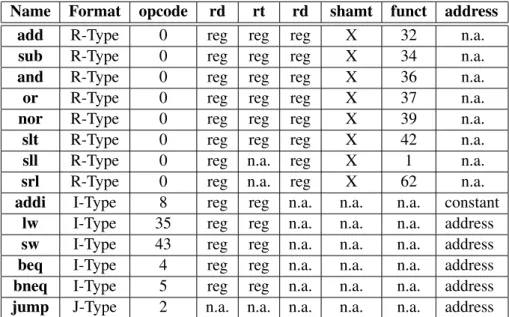
As can be seen in table 3.4, the instructions presented in this work are some of the basic initial MIPS instructions. This reduced instruction set is thought to be enough to provide the understanding of the mechanisms inherent to the MIPS architecture. The instruction set com-prises arithmetic operations as add, sub, addi (add immediate) and slt (set less then), the logical operations and, or, nor, sll (shift left logical), srl (shif right logical), the conditional branch in-structions beq (branch if equal), bneq (branch if not equal), the data transfers inin-structions lw (load word) and sw (store word) and finally the unconditional jump instruction. The nop instruction is not referenced in the instruction set although it is performed by the processor. The shift operations (sll and srl) were established as a one bit shift instead of the original variable bit shift. In order to distinguish these operations from the originals, the opcode is different, being respectively 1 and 62 (the bitwise not). The reasons that led to the implementation of the one bit shifting instructions, instead of the original variable bit shifts, refer to the absence of correspondent hardware descrip-tion in the reference text book and to the fact that, from the ALU from of view, the one bit shifting instructions are faster to perform.
Name Format opcode rd rt rd shamt funct address
add R-Type 0 reg reg reg X 32 n.a.
sub R-Type 0 reg reg reg X 34 n.a.
and R-Type 0 reg reg reg X 36 n.a.
or R-Type 0 reg reg reg X 37 n.a.
nor R-Type 0 reg reg reg X 39 n.a.
slt R-Type 0 reg reg reg X 42 n.a.
sll R-Type 0 reg n.a. reg X 1 n.a.
srl R-Type 0 reg n.a. reg X 62 n.a.
addi I-Type 8 reg reg n.a. n.a. n.a. constant lw I-Type 35 reg reg n.a. n.a. n.a. address sw I-Type 43 reg reg n.a. n.a. n.a. address beq I-Type 4 reg reg n.a. n.a. n.a. address bneq I-Type 5 reg reg n.a. n.a. n.a. address jump J-Type 2 n.a. n.a. n.a. n.a. n.a. address
Table 3.4: Adopted Instruction Set. X stands for “don’t care”, n.a. stands for not applicable. Based in MIPS Instruction Set [2]
3.4
Implemented Processor Models
In this section, the processor versions will be presented and discussed. There will be performed a simple and basic explanation since the objective of this work is not to rewrite the reference text
3.4 Implemented Processor Models 23
Figure 3.2: Unicycle, based in [2].
book. However, and in case of being the first contact of the reader with this architecture, a further reading of reference text book is advised. For the reader understanding interest, the Unicycle will be firstly approached expecting to be the basis for the following processors explanation.
3.4.1 Unicycle
The Unicycle stands for a single cycle per instruction and its design is basically composed of a Program Counter, a Register File, a Control Unit, a ALU and two memories. There are some sup-plementary arithmetic and logical blocks inherent to the processor operation and control flow. All the blocks are asynchronous except the PCounter. In each performed clock cycle, the PCounter is updated with the address of the instruction to be executed. In the same clock cycle, the instruction is executed and a new value is supplied to the PCounter input. This action allows the PCounter to be updated with the instruction expected to be executed in the following clock cycle. Figure3.2 illustrates the Unicycle design.
From the left to the right, as the instruction execution takes place, it can be observed the PCounter, the Instruction Memory where the instructions are stored, the bank of the registers, the ALU whose role is to perform the arithmetic-logical calculations and, at the end of the dat-apath, the data Memory. In the previous chapter it was explained the three groups in which the
24 System Specifications
instructions are classified. All these instructions have two steps in common, preceding the rest of the specific actions needed to complete each instruction execution. The first of the common steps consists of providing the PCounter content to the Instruction Memory address and conse-quently instruction fetch. The second step consists of reading the registers. All the instructions, besides jump, require a read from the register file and an ALU operation. For the present instruc-tion set, the immediate type instrucinstruc-tion addi, the load instrucinstruc-tion lw and the arithmetic shifts sll and srl require only one register read whereas the rest of the instructions require reading two reg-isters. The data transfer instructions require the ALU for address calculation (the ALU adds the register content with the address field content) whereas the arithmetic-logical instructions perform the correspondent function with the content present at the two ALU inputs.
Signal R-format lw sw branche branchNe jump
RegDest 1 0 x x x x ALUSrc 0 1 1 0 0 x MemtoReg 0 1 x x x x RegWrite 1 1 0 0 0 x MemRead 0 1 0 0 0 x MemWrite 0 0 1 0 0 x Branche 0 0 0 1 0 x BranchNe 0 0 0 0 1 x ALUOp1 1 0 0 0 0 x ALUOp0 0 0 0 0 1 x Jmp 0 0 0 0 0 1
Table 3.5: Control Unit table. x stands for “dont’t care”. Based in [2]
After the ALU stage, the load and store instructions need to access the memory to respectively read and write. The store instruction finishes the execution, whereas the load instruction needs additional write-back step, storing the loaded value into the register file. The arithmetic-logical instructions finish the same way as the load instruction, yet, without performing any memory ref-erence. The branchs complete their execution after the equality test performed in the ALU, by selecting the next PCounter content. The jump instruction does not need any additional processing after the instruction decode, but a simple 2bit shift of the address field. This shift is commonly performed in all address calculation concerning the byte addressable memory present in the MIPS architecture. Differently from the branchs address calculation, where the address is obtained rela-tively to the present PCounter, the jumps perform a PCounter update with the value present in the instruction address field. The presented data flow is controlled by a module, which coordinates the processor modules. The Control Unit, a pure combinational block, decodes the instruction opcode and enables the necessary signals so the memories, the register file and necessary multiplexers can perform the requested operations. The control can be defined as:
• RegDst, which selects the register file address source. This control signal is necessary since the instruction set comprehends more than one instruction type. For example, in the R-Type
3.4 Implemented Processor Models 25
instructions, the write register input most be supplied with the Instruction [15 - 11] bits, while in the I-Type load instruction, the correct bits to be handed are Instructions [20 - 16]; • Jump, which selects the destination address to be available at the PCounter input;
• BranchNe and Branche, along with the ALUZero signal, enable the address branch propa-gation;
• MemRead, enables data memory read;
• MemtoReg, selects the input data for the register file write data port;
• ALUOp, along with the instruction function field determines the operation to be performed by the ALU;
• MemWrite, enables data memory write;
• ALUSrc, defines the value to be provided to one of the ALU inputs. This ALU input requires two different sources due to the arithmetic operations performed with both R-Type and I-Type.
• RegWrite, enables the register file write;
The ALUOp and the instruction funct field are propagated into the ALU control block to be decoded, so the ALU control signals can be set. The encoding of the three control signals can be observed in table3.5, and3.6.
Instruction
ALUOp function field desired action ALU
Operation control input
lw 00 X add 0010 sw 00 X add 0010 addi 00 X add 0010 branchE 01 X subtract 0110 branchNe 01 X subtract 0110 add 10 100000 add 0010 subtract 10 100010 subtract 0110 and 10 100100 and 0000 or 10 100101 or 0001 nor 10 100111 nor 1100
slt 10 101010 set on less than 0111
sll 10 000001 shift left 0011
srl 10 111110 shift right 0100
Table 3.6: ALU Control table. X stands for “don’t care”. Based in [2]
Some changes were performed to the reference text book design to support the execution of BranchNe instruction. These modifications can be observed at the top right area of the figure3.2.
26 System Specifications
Instruction Instruction Register ALU Data Register
Total Class memory read operation memory write
R-Type 200 50 100 0 50 400ps
Load word 200 50 100 200 50 600ps
Store word 200 50 100 0 0 550ps
Branch 200 50 100 0 0 350ps
Jump 200 0 0 0 0 200ps
Table 3.7: Instructions length, based in [2].
Two logic gates, a nor with one negative input and an or, were added to the original design in order to support the BranchNe operation. The output select signal of the multiplexer, which supplies the PCounter input, is set by the signal derived from the logic gates. When the ALU Zero value is "0" and the control BranchNe value is "1" the multiplexer outputs the branch calculated address.
3.4.2 Multicycle
The reason that led to evolve to a new architecture conception is based in the Unicycle timing inefficiency. Table3.7presents, hypothetical propagation delays required for each hardware block to perform the desired operation. In the Unicycle version, the clock period is determined by the time of the longest instruction, which is the load word and takes 600ps. The inefficiency problem can now be easily realized: the quicker instruction,(jump), should take only 200ps to be performed, but as a result of the hardware design, it must take the same time as the rest of the instructions, 600ps. The perfect approach would consider a variable clock so each instruction could be executed without overhead. If a mix of instructions (25% loads, 10% stores, 45% ALU instructions, 15% branches and 5% jumps) is considered, the average time per instruction would be [2]:
600 × 25% + 550 × 10% + 400 × 45% + 350 × 15% + 200 × 5% = 447.5ps
instead of the fixed 600ps provided by the Unicycle. However, such a design comprising a variable-speed clock would be extremely difficult to implement.
In the Multicycle processor version, the Unicycle inefficiency does not occur, since the in-struction is broken into several shorter steps being executed one step per clock cycle. Each step is restricted to at most one ALU operation or one register access, or one memory access. The clock period of the Multicycle is therefore determined by the longest step, which in this instruction set takes 200ps. These steps will be addressed after the Multicycle architecture presentation so it can be easily understood by the reader.
The Multicycle Processor architecture is quite different from the Unicycle. As can be illus-trated in figure 3.3 the control signals are not exactly the same, there is a single memory and, besides the ALU, there are no supplementary arithmetic blocks for address computing. Since
3.4 Implemented Processor Models 27
there are no supplementary arithmetic blocks, the ALU must perform all the arithmetic operations as well as, the next address calculation. This, required the presence of a 4 way multiplexer at the ALU lower input. The use of less complex hardware to perform the same instruction set rep-resents another advantage when comparing to the Unicycle. Due to the existence of only single memory it must be shared by instructions and data, requiring an multiplexer at the memory address input. Another difference is the existence of registers between combinational blocks. This register set comprehends the Instruction register, the Memory data register, both registers A and B and a register at the end of the ALU, namely ALUOut. The necessity of using these registers resides in the fact that each clock cycle can accommodate at most one functional operation, and therefore, the data produced by any of the functional units (memory, register file or ALU) must be tempo-rary stored. In the upper part of the schematic it can be observed an or gate, an and gate and a multiplexer. The multiplexer does not appear in the reference text book design, since no branchNe instruction was described. As can be seen, when the branchNe signal is set, the multiplexer selects the not ALUZero signal, which will consequently enable the PCWriteCond control signal. Like in the Unicycle, the PCounter has three different sources. The output of the ALU is PC + 4 during fetch condition, the ALUOut which contains the address in a branch case and the lower 26 bits of the instruction register, shifted two bits to the left1and concatenated with the upper four bits of the incremented program counter (jump case).
The capability to execute instructions in a different number of clock cycles, as well as the ability to share functional units within the execution of a single instruction, requires more than temporary registers. It additionally requires a control unit performing as a finite state machine. The control unit implements eleven control signals which and can be set as [2]:
• RegDst, selects the register file address source; • RegWrite, enables the register file write;
• BranchNe, and Branche, necessary for the branch execution; • MemRead, enables data memory read;
• MemtoReg, selects the input data for the register file write data port;
• ALUOp, along with the instruction function field determine the operation to be executed by the ALU;
• MemWrite, enables data memory write;
• ALUSrcA, selects the source for the upper ALU input. If asserted selects the register A content, if deasserted selects PCounter content;
• ALUSrcB, selects the source for the lower ALU input. If 002selects the register B value, if
012selects the constant 4, if 102selects the lower 16 bit of the instruction register (branch)
and in the case of being 112, it selects the lower 16 bit shifted left by two bits (jump).
28 System Specifications
![Figure 2.4: JVM and JIT Compiler [4]](https://thumb-eu.123doks.com/thumbv2/123dok_br/15880844.1089251/32.892.207.650.334.626/figure-jvm-and-jit-compiler.webp)

![Figure 3.2: Unicycle, based in [2].](https://thumb-eu.123doks.com/thumbv2/123dok_br/15880844.1089251/43.892.154.783.147.629/figure-unicycle-based-in.webp)
![Table 3.5: Control Unit table. x stands for “dont’t care”. Based in [2]](https://thumb-eu.123doks.com/thumbv2/123dok_br/15880844.1089251/44.892.110.740.402.662/table-control-unit-table-stands-dont-care-based.webp)
![Table 3.6: ALU Control table. X stands for “don’t care”. Based in [2]](https://thumb-eu.123doks.com/thumbv2/123dok_br/15880844.1089251/45.892.212.721.703.1020/table-alu-control-table-stands-don-care-based.webp)
![Figure 3.3: Multicycle, based in [2].](https://thumb-eu.123doks.com/thumbv2/123dok_br/15880844.1089251/48.892.111.742.364.869/figure-multicycle-based-in.webp)
![Figure 3.6: Pipeline basic design, based in [2].](https://thumb-eu.123doks.com/thumbv2/123dok_br/15880844.1089251/53.892.148.785.257.603/figure-pipeline-basic-design-based-in.webp)
