690 Brazilian Journal of Physics, vol. 29, no. 4, December, 1999
Ambipolar Carrier Diusion in In
0:53Ga
0:47As
Single Quantum Wells
A.F.G.Monte, S.W.da Silva, J.M.R.Cruz, P.C.Morais,
UniversidadedeBraslia,InstitutodeFsica,Nucleode
FsicaAplicada,70910-900,Braslia-DF,Brazil
and H.M.Cox
LucentTechnologies,MurrayHill,NewJersey07974,USA
Received February 8, 1999
The microluminescence surface scan technique (MSST) has been used to investigate photocarrier diusion in undoped In0:53Ga0:47As - InP single quantum well (QW), in the temperature (T) range
from 15 K to 295 K. Narrowing of the photoluminescence (PL) spatial prole is observed as the temperature is lowered, indicating reduction of the photocarrier diusion length upon cooling. It was found that the width of the PL spatial prole follows a linear function of temperature, but a change in slope by a factor of 2.6 is observed at about 200 K, indicating a change of the dominant carrier scattering mechanism. In the temperature range of 15 K to 200 K, the ambipolar photocarrier diusion mechanism seems to be correlated to impurity states thermally activated.
I Introduction
Investigations of photocarrier transport properties in two-dimensional heterostructures have a great deal of interest, since they play a central role in the design and operation of photovoltaic devices. Experimental tech-niques which incorporate spatial resolution capabilities have been recently developed, being used to investigate the physical processes of light emission and photocar-rier dynamics in semiconductor quantum wells (QW). Cathodoluminescence (CL) [1] and optical beam in-duced current (OBIC) [2] have been extensively used to measure the carrier diusion length. An early study of photocarrier transport used a spatially scanned pump-probe technique for imaging the in-plane motion [3]. The microluminescence surface scan technique (MSST) has been recently applied to study the photocarrier transport mechanism in bulk semiconductors [4]. In the MSST, a tightly focused laser beam is used to excite the sample surface, and the lateral spread of electron-hole pair is observed by scanning the microluminescence im-age at the focal plane of the system. Such a measure-ment allows the determination of the eective diusion length of the photoexcited carriers, which in turn pro-vides indirect information about parameters as
impor-tant as the photocarrier lifetime and the photocarrier mobility. In this work, we use the MSST setup to in-vestigate the transport properties of photocarriers in an undoped single QW of InGaAs lattice-matched to InP, in the temperature range of 15 K to 295 K.
II Experiment
The lattice-matched InGaAs-InP single QW (LV 614) used in this study was grown by Vapor Levitation Epi-taxy (VLE) [5]. The nominally undoped sample con-sists of a 0.6 m InP buer layer epitaxially grown on
top of an InP substrate, followed by a 110 A thick In-GaAs layer, and covered with a 600 A InP cap-layer. The sample was mounted in a temperature-controlled optical cryostat, and optically excited using an Ar+
-ion laser tuned at 514 nm, which provides energy ex-citation above the InP band gap. The laser beam was focused down to a spot of 4m in diameter, thus
allow-ing lateral photoluminescence (PL) measurements with very good resolution. The radial PL intensity distribu-tion is chopped, synchronously amplied and measured using a Nitrogen-cooled Germanium detector, as de-scribed elsewhere [6]. Photoexcitation creates
A.F.G.Monteet al. 691
hole pairs, all across the structure, which are quickly captured by the InGaAs single QW. Following photoex-citation, lateral carrier diusion and spontaneous ra-diative recombination take place, the later is the main source of the PL intensity (I
PL). The optical excitation
intensity was set at a level strong enough to produce carrier density in the range of 1-5 x 1017cm,3, where
carrier recombination is dominated by the bimolecular mechanism. Thus, the recombination rate is given by
Bnp, where B is the bimolecular recombination
coef-cient, n and pare respectively the electron and hole
densities. The PL intensity is given by I PL =
Bnp.
Finally, two main assumptions have been made here. First, the photogenerated carrier density is assumed to be higher than any residual dopant density, and second, the charge neutrality is assumed, so that the photoin-duced hole density is equal to the photoinphotoin-duced electron density.
III Results and Discussions
Fig. 1 shows typical spatial PL distributions, at dier-ent temperatures. The observed PL distribution is usu-ally described within the diusion theory. Since photo-carriers are mainly conned in the InGaAs layer, carrier transport can be well described by the two-dimensional diusion equation, in the steady state regime. The dif-fusion equation that describes the electron density, in polar coordinates reads:
D 1 r @ @r r @n @r
=G(r), n
,Bnp; (1)
whereDis the eective carrier diusion coecient, and is the eective carrier lifetime. G(r) is the
photo-carrier generation term provided by a Gaussian-shaped laser spot, depending only upon the optical excitation intensity. As long as both the linear and quadratic terms are kept in the right-hand side of Eq. (1), nu-merical simulation shows that a Gaussian function rep-resents a good solution for n(r). The carrier diusion
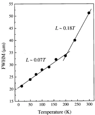
length (L) is then obtained from the simulated curve,
and goes parallel with the full width at half maximum (FWHM) of the spatial PL prole. The temperature dependence of the spatial PL expansion (FWHM) is shown in Fig. 2. Our data show an increase in the width (FWHM) of the spatial PL prole as the temperature increases from 15 K to 295 K. We found the FWHM go-ing with the temperature accordgo-ing to a linear function
T, with= 0:07 in the temperature range of 15 K to
200 K, and= 0:18 in the temperature range of 200 K
to 295 K. The change in the slope of the curve, at about 200 K, is probably associated to the thermal activa-tion of a defect center, as discussed below. A narrower spatial PL distribution, as experimentally observed at low-temperatures, and, consequently, a smaller carrier diusion length, could be attributed to connement of the carriers close to the center of the laser spot due to gap renormalization [7]. However, dierent mecha-nisms can account for the scattering rate and, therefore, for the carrier diusion length, including phonon scat-tering, interface roughness, and impurities [8]. Note that any expansion eventually becomes exponential at large distances, and carrier recombination is dominated by non-radiative interface recombination. Close to the laser spot, however, Coulombinteraction between carri-ers does not allow spatial charge separation, and carrier density reduction is dominated by ambipolar carrier re-combination (Bnp). The most likely mechanism
692 Brazilian Journal of Physics, vol. 29, no. 4, December, 1999
Figure 1. Square root of the PL intensity (I
PL) of the 110
A thick In0:53Ga0:47As SQW for three temperatures. These
data clearly show the spatial expansion of the photoexcited carriers sincen/(IP
L)
1=2. The laser spot diameter on the
sample surface was about 4m (FWHM).
Figure 2. Spatial PL distribution (FWHM) as a function of temperature. The solid line is a t to the experimental data based on a linear temperature dependence. A change in slope would indicate a change of the dominant carrier scattering mechanism.
Figure 3. Total carrier density that recombine radiatively as function of temperature. We observe an abrupt change on the carrier density at about 150 K, which may be associated to thermal activation of an impurity related recombination channel. The solid and dashed lines are only guides to the eyes.
Figure 4 Spatial PL distribution (FWHM) at 13 K as a function of the excitation intensity. The solid line is only to guide the eyes.
IV Conclusions
A.F.G.Monteet al. 693
dominates the carrier diusion process close to the laser spot, and the carrier diusion length increases linearly with the temperature. A change in slope by a factor of 2.6 is observed at about 200 K, indicating a likely change of the dominant carrier scattering mechanism, and appears to be correlated with the thermal activa-tion of a defect center. At low-temperatures, the car-rier diusion length saturates with increasing optical excitation intensity, indicating the presence of a defect-limited carrier diusion.
Acknowledgement
The authors would like to thank nancial support from FAP-DF and CNPq (Brazilian agencies), and Third World Academy of Sciences (TWAS).
References
[1] H.A. Zarem, P.C. Sercel, J.A. Lebens, L.E. Eng, A.
Yariv, and K.J. Vahala, Appl. Phys. Lett. 55, 1647
(1989).
[2] M. Gallant and A. Zemel, Appl. Phys. Lett.52, 1686
(1988).
[3] H.W. Yoon, D.R. Wake, J.P. Wolfe, and H. Morkoc, Phys. Rev. B46, 13461 (1992).
[4] A.F.G. Monte, J.M.R. Cruz, P.C. Morais, and H.M. Cox, Sol. St. Commun.109, 163 (1998).
[5] H.M. Cox, S.G. Hummel, and V.G. Keramidas, J. Cryst. Growth79, 900 (1986).
[6] A.F.G. Monte, J.M.R. Cruz, and P.C. Morais, Rev. Sci. Instrum.68, 3890 (1997).
[7] R. Cingolani and K. Ploog, Phys. Rev. B 42, 2893
(1990).
[8] H. Hilmer, A. Forchel, T. Kuhn, G. Mahler, and H.P. Meier, Phys. Rev. B43, 13992 (1991).
[9] E. Zielinski, H. Shweizer, K. Streubel, H. Eisele, and G. Weimann, J. Appl. Phys.59, 2196 (1986).