Thick CrN/NbN Multilayer Coating Deposited by Cathodic Arc Technique
Juliano Avelar Araujoa, Roberto Martins Souzab, Nelson Batista de Limac, André Paulo Tschiptschina,d*
Received: April 10, 2016; Revised: October 25, 2016; Accepted: November 21, 2016
The production of tribological nanoscale multilayer CrN/NbN coatings up to 6 μm thick by
Sputtering/HIPIMS has been reported in literature. However, high demanding applications, such as
internal combustion engine parts, need thicker coatings (>30 µm). The production of such parts by sputtering would be economically restrictive due to low deposition rates. In this work, nanoscale
multilayer CrN/NbN coatings were produced in a high-deposition rate, industrial-size, Cathodic Arc
Physical Vapor Deposition (ARC-PVD) chamber, containing three cathodes in alternate positions (Cr/ Nb/Cr). Four 30 μm thick NbN/CrN multilayer coatings with diferent periodicities (20, 10, 7.5 and 4 nm) were produced. The coatings were characterized by X-Ray Difraction (XRD) and Transmission Electron Microscopy (TEM). The multilayer coating system was composed of alternate cubic rock-salt CrN and NbN layers, coherently strained due to lattice mismatch. The ilm grew with columnar morphology through the entire stratiied structure. The periodicities adopted were maintained throughout the entire coating. The 20 nm periodicity coating showed separate NbN and CrN peaks in the XRD patterns, while for the lower periodicity (≤10nm) coatings, just one intermediate lattice (d-spacing)
was detected. An almost linear increase of hardness with decreasing bilayer period indicates that
interfacial efects can dominate the hardening mechanisms.
Keywords: NbN/CrN, Multilayer Coatings, Cathodic Arc, Nanostructure
* e-mail: [email protected]
1. Introduction
The CrN is a classic coating system, which is technologically relevant since the early 1980’s1-5. The high hardness and
lower friction coeicient, when compared to other piston
ring system coatings2,6,7, has drawn engineer’s attention
to the use of this kind of coating for internal combustion
engine components. Currently, it is applied in large scale for piston rings2,5. While typical applications may not require
the PVD coating thickness to be above 6 µm 5, it frequently
needs to be on the order of 30 µm when the PVD layer is
deposited onto a combustion engine component5-7. Such
high thickness is mandatory when considering the highly
demanding environment of internal combustion engines, which is associated to high wear rates8. Furthermore, the
increasing combustion pressures and the reduced lubrication oil availability found in new generation engines require additional toughness and wear resistance to avoid damage of the parts.
In recent years, multilayer CrN/NbN coatings have attracted Engineer’s attention, since the niobium nitride
component (NbN) stands out for its chemical stability8
and the chromium nitride (CrN) is a hard and inert coating
component2,3, ofering the temperature resistance required
for working in the combustion chamber environment. NbN/
CrN nanostructured multilayer coating combines high hardness with chemical stability and toughness. Besides that, Munz et al.9 have reported a superior wear resistance
of CrN/NbN multilayer coatings over single layer coatings and electrodeposited chromium. Most of CrN/NbN coatings studied were produced by sputtering process, with or without an interlayer produced by cathodic arc evaporation10-14. In a few cases15, the coatings were entirely produced by the
cathodic arc technique, as in this work. Many CrN/NbN PVD coatings described in the literature are up to 6 µm thick, which makes them inappropriate for applications
that require long-term high wear resistance, such as internal combustion engine parts. The issues in achieving larger
thicknesses using sputtering include the diiculty in keeping
the multilayer periodicity through the entire coating, due to target poisoning. Many authors have studied the relationship
between structure and mechanical properties of diferent PVD sputtered multilayer coatings with typical thickness a Metallurgical and Materials Engineering Department, University of São Paulo – USP, Av. Prof. Mello
Moraes, 2463, ZIP 05508-030, São Paulo, SP, Brazil
b Mechanical Engineering Department, University of São Paulo – USP, Av. Prof. Mello Moraes, 2231,
ZIP 05508-030, São Paulo, SP, Brazil
c Department of Materials Characterization, Nuclear and Energy Research Institute – IPEN, Av. Prof.
Lineu Prestes, 2242, CEP 05508-900, São Paulo, SP, Brazil
d Brazilian Nanotechnology National Laboratory – LNNano, Brazilian National Center of Research in
between 2-5 µm, relating such properties to the periodicity (Ʌ) and the interface morphology12,16-18.
Hovsepian et al.19-21, Munz et al.9,12 and Tomlinson et
al.14 have reported the characterization of multilayer CrN/ NbN coatings, particularly pointing out the advantages of
using arc bond sputtering (ABS). The results showed that the position of CrN and NbN X-ray difraction peaks represented the weighted mean of the individual relections of the CrN
and NbN phases. According to the authors, the occurrence
of satellite peaks demonstrated the superlattice nature of the
coating structure. Additionally, Hovsepian et al.22 produced
CrN/NbN by three diferent PVD techniques (ABS, UBM and ARC) and showed that, despite the low bias voltage of ARC process, there is an increase in ion energy up to 300 eV.
This value resulted in an increased adatom mobility, when
compared to 120 eV for UBM, which suppresses interface roughness efects and may produce a smoother interface
between individual CrN or NbN layers. CrN/NbN deposited
by ARC showed the lowest friction coeicient and highest
wear resistance, when compared to CrN/NbN produced by sputtering processes.
Lewis et al.23 grew CrN/NbN by UBM in diferent bias voltages and found up to 14% reduction in periodicity throughout the multilayer in coatings 1.4 µm thick. The reduction was consistent for 3.0 µm thick coatings as well. The periodicity reduction was justiied by the increase of
target poisoning with time.
Wang et al.24,25 studied the corrosion and wear resistance of NbN/CrN coatings produced by ABS. They showed that
the coating must be substantially thicker than the size of
the macroparticles causing wear, in order to mitigate their
efects on the NbN/CrN coating performance.
Pecchio15, Bemporad13, Ceschini26, Martini27 and Pilone28
have studied NbN/CrN coatings entirely produced by arc processes. These coatings were produced using the switch cathodic arc evaporation technique, which is characterized by alternate triggering of the Cr or Nb cathodes. These coatings showed better wear performance than CrN single-material coatings produced by the same process.
It is important to notice that the research works mentioned above were centered on coatings with thickness lower than 6 μm. In terms of deposition processes, cathodic ARC has
industrial interest due to its high deposition rate when compared to sputtering. The later would be economically restrictive when one compares the deposition rate of Sputtering/HIPIMS
(~1.2 µm/hr)23,29 with ARC (~3.0 µm/hr)13.
This work explored and found features never presented before. One example is the high coating thickness - in the order of 30 µm, since coatings with such thickness were reported only in a previous work by the authors33. In addition to the
technological beneit, extending service life of components, the thick coatings in this work allowed exploring some features
of the cathodic arc technique such as the evolution of the coating structure during the deposition process. In this case,
the results conirmed the trend for a particular preferential
crystallographic orientation depending on periodicity, but,
diferent from sputtered coatings found in the literature,
the deposition conditions remained similar with deposition time, ensuring that a consistent value of periodicity was
obtained along the entire coating thickness of each deposition
process. Another important point of the cathodic arc process is the presence of macroparticles, which have caused local changes in the structure. However, the amount of macro particles, and the associated loss of parallelism of the layers with the coating/substrate interface, has not prevented the
use of characterization techniques such as kinematic X-ray difraction to calculate periodicity based on the position of satellite peaks.
In this work, gas nitrided martensitic stainless steels
coupons were PVD-coated using the cathodic arc process. The
30 µm-thick NbN/CrN multilayer coatings were deposited with various periodicities but keeping the same periodicity along the entire coating thickness. The aim of the investigation
was to characterize the microstructure, periodicity along all
coating thickness and the relationships between microstructure and hardness for such thickness values.
2. Experimental Procedure
NbN-only and CrN-only coatings, as well as NbN/CrN
multilayer coatings with diferent periodicities (Λ varying from 4 to 20 nanometers), were deposited onto gas nitrided martensitic stainless steel (AISI 440B) coupons.
Substrate Preparation and Cleaning - The steel strip was
ground and diamond polished, keeping the surface roughness before deposition below Rz = 0.5 μm. Before being placed
in the deposition chamber, the coupons were chemically
cleaned in two diferent stages. The irst stage consisted in
the use of a degreasing agent, Renoclean® 237, for removal
of inorganic and organic residue, while the second stage consisted in ultrasonic rinsing with deionized water.
Coating Deposition - Depositions were conducted in an industrial cathodic arc physical vapor deposition equipment
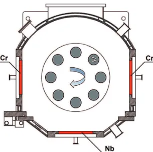
(Hauzer Techno Coating Europe B.V., model HTC750). Figure
1 shows the schematic drawing of the cross section of the equipment displaying the cathode positions. The chamber
has three rectangular cathodes (working area of 1200 cm2),
each one capable of working independently and having its
own power supply.
The multilayer periodicity was controlled by varying the rotating speed of the table and consequently the time that the specimens pass in front of each target without shield/ shutter. The specimens were placed facing the targets in a two-fold rotating table, at a distance of 10 cm from the
substrate. The table rotated around the vertical axle of the
reactor and each specimen rotated around its own center, to ensure a homogeneous deposition on top of the entire
Measurements of the total thickness of the coatings were conducted using a FEI Quanta 600 – FEG scanning
electron microscope. Additionally, qualitative and semi-quantitative chemical composition assessments of all the
coatings were carried out using energy-dispersive X-ray spectroscopy (EDS). The crystallographic structures of the multilayer coatings were determined by X-ray difraction using a Multilex Rigaku difractometer. A coniguration of Bragg-Brentano θ-2θ, copper Kα radiation (1.5418 Å) and 2θ angles varying from 20o to 120o with an interval of
0.02o and 2 seconds of integration time per point was used.
The coatings were also characterized by Transmission
Electron Microscopy (TEM) for quantitative analysis of
the nanostructured multilayer constituents and assessment
of their relative thicknesses and diameter of polycrystalline
columns. High Resolution Transmission Electron Microscopy
(HRTEM) was used to assess a qualitative evaluation of the interfaces between the sub-layers. For this purpose, thin foils were prepared using an FEI Helios 660 Focused Ion Beam (FIB) scanning electron microscope. In order to carry out the TEM analysis across the 30 µm thick coatings, it was used a 200 kV TEM Philips CM20 microscope equipped with an EDS Voyager Noran analyzer (high purity Ge detector and ultra-thin window - UTW). The high resolution images were acquired with a 300 kV HRTEM JEOL 3010. The electron difraction analysis was conducted following the procedure
published by Zuo et al.31 and provided information about the
crystal structure of individual sub-layers (NbN and CrN), the orientation of the (hkl) planes and the preferential direction
of crystal growth.
A Micro Combi Tester with instrumented indentation
system (maximum normal loads up to 500 mN) and a Hysitron TI950 (30 s load/unload and maximum normal load up to 10 mN) were used to assess the coating microhardness, according to the ISO standard 14577-4 – Edition 2007. The hardness
measurements were conducted on the polished coating cross section. The instrumented microindentation results presented
in this work are an average of ive measurements. The number of nanoindentations in each sample was signiicantly higher (over 200) and aimed at measuring hardness along the entire coating thickness.
3. Results and Discussion
3.1. Microstructure of single layer coatings (NbN
or CrN)
The structure of individual NbN and CrN coatings depends mainly on the nitrogen partial pressure, the bias
voltage and the total pressure. Transition metals nitrides exist in diferent allotropic forms with diferent stoichiometries. For instance, nitrides composed of Nb and N can present the
following chemical compositions and crystalline structures:
Figure 1: Schematic drawing of the cross section of the HTC-750
coating chamber, showing the target/cathodes positions.
times, leading to the formation of coatings with periodicities
of 20 nm, 10 nm, 7.5 nm and 4 nm.
The substrate was heated to 400 oC, a loating bias
voltage was applied and the maximum output was 120 W/
cm2 for each cathode. Before the deposition of the coatings,
the substrates were ion cleaned with Cr targets switched on
(metal ion cleaning) in Ar atmosphere.
The average deposition rate was 3 µm/h, as detailed below, and the total thickness of the multilayer coatings was 30 μm, in all cases.
The deposition process consisted of three stages: 1. Ion cleaning using a bias voltage of -900 V. 2. Deposition of a metallic chromium bonding layer
under argon atmosphere, with total pressure lower than 10-3 mbar and using a substrate bias voltage of -20 V.
3. Deposition of multilayer coatings by simultaneous operation of all three targets. During the whole
deposition process, the total pressure was kept at 3x10⁻³ mbar and the ratio between argon and nitrogen
was kept at 0.25. The electric current applied to
niobium and chromium targets was balanced aiming an atomic ratio of Nb/Cr = 0.8. The total time for
efective deposition was 9.5 hours.
The superlattice periodicity is controlled by the power dissipated on the targets, the partial pressure of the reactive gas, the bias voltage applied to the substrate and the primary rotation speed of the turntable.
After deposition, cross sections of the coatings were
β-Nb2N (hexagonal), γ-Nb4N3 (tetragonal), δ-NbN
(face-centered cubic), δ’-NbN (hexagonal), ε-NbN (hexagonal), η-NbN (hexagonal), and α-Nb(N) a solid solution formed by
metallic Nb containing solubilized N11. Additionally, nitrides
composed of Cr and N can appear as: CrN (face-centered cubic) and Cr2N (hexagonal)
5.
Chromium-based (chromium, CrN, CrC and Cr-C-N)
hard coatings produced by PVD have been used successfully
in tribological systems where corrosion, oxidation and intense wear are expected. These coatings came out as
replacements for electroplated hard chromium in some applications; fcc-CrN coated piston rimgs, have been used successfully in heavy internal combustion engines. The aim of combining chromium with niobium as the chemically stable metal is to enhance the corrosion resistance of the coating
and to increase hardness values to 40 GPa, by utilizing the superlattice efect20. A multilayer coating containing
alternate layers of two isostructural phases (fcc - δ-NbN and fcc - CrN) with a small diference in lattice parameter,
can give rise to coherency strains/stresses responsible for the strong hardening. Accordingly, NbN/CrN depositions
were made with settings chosen to properly obtain δ-NbN (face-centered cubic) and CrN (face-centered cubic) nitrides.
Given that the energy of formation of fcc δ-NbN (ΔH298
= 56,8 Kcal/mol) and fcc CrN (ΔH298 = 29,8 Kcal/mol) difer
signiicantly, adjustment of the deposition parameters of
the cathodic arc process is mandatory in order to allow the formation of a multilayer coating constituted only by the
two fcc phases, δ -NbN and CrN. After optimization of the
deposition parameters, individual NbN and CrN coatings
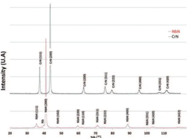
were produced and analyzed by X-ray difraction in the θ-2θ geometry, resulting in the X-ray difraction patterns shown in Figure 2.
Figure 2 shows that both NbN and CrN phases have a face centered cubic structure with a (200) preferred orientation.
The d-spacings are the same as those indicated on ICDD cards
#38-1155 and #11-65, respectively, giving lattice parameters of 0.439 nm for NbN and 0.415 nm for CrN, thus producing a diference around 5.5% between the two parameters. These parameters also suggest that there is no nitrogen excess in
the coating structures32 and that no signiicant peak shifts due to coating residual stresses were observed in these cases.
The additional lines, visible in the difraction patterns of NbN refer to Nb droplets. The X-ray difraction patterns in Figure 2 were considered “standards” for individual NbN
and CrN lines that could be used in comparison with those
obtained with the multilayer difraction pattern.
3.2. Microstructure of the multilayer coating
Figure 3 shows a low-magniication photograph of the surface of a 4 nm periodicity coating. The ARC coating process leads to the formation of a signiicant amount of
droplets on the top of the coated surfaces. The use of these
Figure 2: X-ray difraction patterns of NbN and CrN coatings,
containing information about the phases and crystallographic planes.
Figure 3: Observation of the coating surface of a 4 nm periodicity
coating at low magniication. SEM (SE image).
coatings for tribological applications requires grinding and polishing after deposition. These macroparticles are present during the entire deposition and they can also interfere with the growth of the nanoscale multilayer coating. This was
not the case in this work, as detailed later.
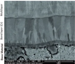
Figure 4 shows the Cr bonding layer, with an average thickness of 1 µm, and its columnar structure. Figure 4
provides preliminary evidence that the NbN/CrN structure is constituted of uniform and well-spaced alternate layers of
NbN (light) and CrN (dark). Figure 4 also indicates a dark
layer below the chromium layer, most probably formed due
to ion etching and chromium difusion.
Figure 5 shows the θ-2θ X-ray difraction patterns for all four NbN/CrN multilayer coatings with diferent periodicities.
of two sublayers. The central peak position represents the
average d-spacing between the sublayers, corresponding to the weighted average between the d-spacing of each sublayer component, and being calculated using equation 1:
Figure 4: SEM – vCD (low voltage high contrast detector). Detail
showing the base material, the chromium bonding layer and the NbN/CrN multilayer coating.
Figure 5: X-ray difraction patterns of the four NbN/CrN multilayer
coatings with periodicities of 4 nm, 7.5 nm, 10 nm and 20 nm. In the same image, the full lines in red and black indicate the positions corresponding to NbN and CrN, ICDD #38-1155 and ICDD #11-65 cards, respectively in the (111) and (200). The dotted line, identiied by “I”, corresponds to the intermediate peaks of the 10 nm, 7.5 nm and 4 nm periodicity multilayer coatings. “sa” are the satellite peaks around the central peak in the (200) position.
For the smallest periodicity studied in this work, the
lattice parameters of the NbN and CrN sublayers change
towards a common intermediate value (Figure 5). The development of a (200) texture on NbN/CrN coatings
can be seen with periodicities smaller than 10 nm, especially
for 4 nm periodicity coating. Moreover, the difraction patterns show a strong central peak, and a group of satellite peaks on its vicinities with gradually decreasing intensities. The central peak is located at 2θ = 42.5°, and the irst order satellite peaks are visible at both sides of the central peak,
as predicted in the literature33-35.
Periodicity and average d-spacings for the coatings thinner than 10 nm were calculated based on the formulation
described by Segmüller and Blakeslee36. Following this
procedure, equation 2dsini=nm identiies Bragg’s central
peak position related to the multilayer and K=QNA+NBVd
determines the modulation period. In these equations, N is the average number of planes and Ʌ is the periodicity
( )
d
N
N
N
d
N
d
1
NbN CrN
NbN NbN CrN CrN
=
+
+
The multilayer modulation period, calculated based on
the position of satellite peaks is given by equation (2), where m and n are integers that represent the order of the satellite
peaks chosen for Λ calculation
( )
sin
sin
m
n
2
2
sat
m n
/
=
Q
i
-
V
-
m
Q
i
V
The identiication of these parameters has been conducted with the help of the program SLERFWIN by G. Gladyszewski37. This software considers the Monte Carlo
approach for modelling imperfect multilayers and is based
on kinematic X-ray difraction. The program was used to simulate X-ray patterns, which were latter compared with the difraction patterns obtained experimentally. Figure 6
presents this comparison for the NbN/CrN sample with a
periodicity of 4 nm and 7.5 nm, indicating a good match between simulated and experimental data.
Figure 6: Experimental and calculated (using the SLERFWIN
software) X-ray difraction pattern in the (200) region, for NbN/ CrN multilayer samples with a periodicity of 4 nm and 7.5 nm.
Table 1 shows the structural parameters selected for
Table 1: Periodicity values and sublayers thickness as calculated by the SlerfWin Program for Λ =4.0 nm and 7.5 nm) and values measured
by HRTEM for Λ from 4 to 20 nm.
X-Ray (calculated) HRTEM (measured)
4 nm 7.5 nm 4 nm 7.5 nm 10 nm 20 nm
Periodicity 3.6 7.2 4.0 7.7 10.5 20.7
NbN sub-layer (nm) 1.7 3.2 1.9 3.6 4.7 9.6
CrN sub-layer (nm) 1.9 4.0 2.1 4.1 5.8 11.1
experimentally measured values, one can see diferences smaller than 10%, indicating a good it.
The analysis of the microstructures by TEM indicates that all four coatings were formed by deposition of alternate CrN and NbN sublayers with decreasing periodicities of
about 20.7 nm, 10.5 nm, 7.7 nm and 4.0 nm. Due to the high total thickness of the coating, the inspection of the whole coating structure was conducted on diferent areas lying at diferent depths. It was observed that the sublayers thickness variation along the total coating was smaller than 7%. Thus,
the microstructure was found to be homogeneous along the
whole coating thickness, conirming that the control of the rotating speed of the table is an efective tool to control the sublayer thickness. In comparison with sputtering-deposited
NbN/CrN coatings20,23, the coatings deposited in this work do not present an evident decrease in bi-layer period as the
overall thickness increases, Figure 7. This decrease was
observed by Lewis23 and was explained based on: (i) texture
development and re-sputtering rate and (ii) target poisoning
throughout the process. The consistency of the bi-layer
periodicity along the coatings obtained in this work may be a result of (i) not only the characteristics of the cathodic arc process, in which the efect of target poisoning is not
comparable with those of the sputtering processes, but also
(ii) the use of lower bias voltages (-20 V in comparison with -75 to -150 V).
In addition, a signiicant technological advantage results from this methodology, since all targets (Niobium and Chromium) work at the same time during the deposition
process, optimizing the deposition rate and consequently reducing the coating manufacturing cost. High deposition
rates, typical of the cathodic arc process (~3 µm/h13 against
~1 µm/h for sputtering23,29), were achieved. Moreover, the
Figure 7: Bright-ield micrographs of the cross-section of the NbN/CrN multilayer coating with periodicity of ~20 nm taken (a) near the
interface; (b) at the middle of the coating and (c) near the surface.
deposition parameters selected in this work allowed the deposition of 30 μm thickness coatings, which are much larger than the reported similar multilayer systems below 7 μm 20,23. The deposition of coatings with thickness above 30
µm may be mandatory in some applications; for example,
in components for internal combustion engines, which are
associated with operations over extended periods of time 6,7.
Figure 7 also shows that NbN and CrN sublayers follow
the irregularities of the surface of the substrate, as well as those due to the presence of metallic Nb and Cr macroparticles
(droplets) deposited during the cathodic arc process. It is noted that these macroparticles afect neither the periodicity nor the individual layer thickness.
The columnar microstructure (with variable column widths between 50 nm and 100 nm) overlaps the multilayer
structure maintaining the same orientation by a mechanism of
localized epitaxial growth. The width of these columns may increase or decrease along the coating thickness, according
to the simultaneous growth rule9.
Figure 8 shows a TEM image displaying the multilayers with their respective selected area difraction patterns. This
image indicates that both phases are face-centered cubic
(fcc) and textured in the [002] direction.
A double spot can be observed in the area highlighted
in Figure 8b, representing the two crystals of the NbN and CrN sublayers. They exhibit similar orientation with slightly diferent lattice parameters, indicating epitaxial growth of
the sublayers.
Figure 9 shows a HRTEM image of the multilayer
coating, at the earliest stages of the growth on top of the Cr interlayer. Although there is no parallelism between atomic
planes of the Cr interlayer and the irst deposited NbN
Figure 8: TEM image of a ~10 nm multilayer coating, with its respective Electron difraction pattern. (a) The micrograph shows the
region used for acquiring the difraction patterns. (b) Electron difraction pattern obtained from an area (diameter 50 nm) enclosing both NbN and CrN layers and difraction spots from individual NbN and CrN layers (c and d, respectively).
Figure 9: HRTEM image of the multilayer coating, at the earliest stages of growth on top of the Cr interlayer. NbN/CrN coating with periodicity of 20 nm.
planes of the subsequent CrN and NbN sublayers and even
localized epitaxy.
The NbN and CrN layers could be related to coherence stresses and hardness, which increases as the periodicity
decreases. Although the presence of metallic Cr and Nb macroparticles caused a disorder in the layer regularity, it was possible to detect the formation of superlattice, satellite
peaks on coatings of 7.5 and 4 nm.
3.3. Microhardness and periodicity
Nanohardness measurements were performed along
the entire coating thickness, from surface to base material. Figure 10 presents the plotted nanohardness proile along the entire 30 µm thickness of the 20 nm periodicity NbN/CrN.
These measurements were performed in order to illustrate
that no signiicant variation in hardness was detected along the thickness of the NbN/CrN multilayer coatings. Local
variations in hardness values can be attributed to the presence of macroparticles on the coating.
Since Figure 10 indicates that no hardness variation occurs along the thickness of the NbN/CrN multilayer
coatings, microhardness measurements were performed on
polished cross sections of multilayer coatings with diferent periodicities, in order to investigate the efect of the multilayer
Figure 10: Nanohardness proile of NbN/CrN multilayer coating
(Ʌ= 20 nm) as a function of coating thickness.
Figure 11: Hardness variation as a function of NbN/CrN multilayer coating bilayer periodicity.
are presented in Figure 11. This plot includes values obtained
with specimens with other periodicities than the four detailed
in this work, but produced following the same procedure. Figure 11 indicates that hardness increases as the periodicity decreases from 20 nm to 4 nm. This result is in agreement with previous works41-43, which reported hardness values 2-3
times greater for polycrystalline nitride multilayer coating
(TiN/NbN) than for those of homogenous TiN and NbN.
In the 1970’s, Koehler suggested that a multilayer coating composed of two diferent materials with the same crystalline
structure would result in a material with very high hardness and toughness, since the interfaces would act as barriers for dislocation movement41. Some decades later, Sproul et al.42 stated that several explanations have been proposed to explain the hardness increase, including not only the
dislocation barrier due to the interface mismatch43 but also
the Hall Petch efect44. Additionally, coherent strain and the
efect of diferent modulus of elasticity between sub-layers
have been suggested as mechanisms that may contribute
for hardness increase. More speciically, Hultman et al.45
investigated the TiN/NbN system and concluded that plastic deformation and dislocation movement are limited within
each sublayer during a scratch test. The hardening efect was once again attributed to the dislocations coninement
between the sub-layer interfaces.
Following the concepts presented previously, the hardening efect in multilayer coatings with periodicity around 10 nm and below can be explained by the presence of several sublayers and by the diferent lattice parameters
of each sublayer. The NbN lattice is around 4% larger
than the CrN lattice. The presence of the sublayers forces the crystallographic planes to align, thus reducing the
diference between lattice parameters of each sublayer, which is adjusted by elastic stresses. These stresses diicult
dislocation movement across the interface. In multilayer coatings with periodicity values greater than 10 nm, the stresses are increasingly relieved within the sublayers,
due to the presence of interfacial misit dislocations and
semi-coherent interfaces9,46.
4. Conclusions
NbN/CrN nanostructured multilayers were manufactured
by PVD (ARC process). The X-ray analysis combined
with computer modeling, allowed the determination of the multilayers periodicity and the d-spacing for NbN and CrN
sub-layers. Furthermore, columnar structures with the same
crystallographic orientation were formed.
The homogeneity of periodicity throughout the coatings
conirms that the deposition rate of CrN and NbN is stable and
that the substrate rotation is the main variable in this control. A technological advantage results from this methodology,
since both targets (niobium and chromium) work at the
same time, improving the deposition rate and reducing the manufacturing cost.
As the coating thickness increases, the sublayer surface
becomes more irregular , due to the accumulation of defects and macroparticles. Thus, for engineering applications,
surface inishing after coating deposition is required in order
to control the roughness.
The modulation periods for those multilayers as
determined by X-rays were similar to those measured by Transmission Electronic Microscopy (TEM). When combining the TEM with high angle X-rays analysis, it
can be concluded that this last technique is a useful and simple tool to measure the periodicity of nanostructured multilayer coatings, even in coatings prepared by cathodic arc.
The hardness increase observed for the NbN/CrN system is in agreement with the literature, showing that despite the typical discontinuities of the cathodic
arc processes, it was possible to take advantage of the
combination of nanostructured multilayers.
5. Acknowledgements
The authors acknowledge the financial support from the São Paulo State Research Foundation, FAPESP,
processes n. 2012/50890-0, and from National Research
National Laboratory at CNPEM – Brazilian National
Center of Research in Energy and Materials for the Electron Microscopy Measurements.
6. References
1. Aubert A, Gillet R, Gaucher A, Terrat JP. Hard chrome coatings
deposited by physical vapour deposition. Thin Solid Films.
1983;108(2):165-172.
2. Mayrhofer PH, Willmann H, Mitterer C. Oxidation kinetics of sputtered Cr–N hard coatings. Surfaceand Coatings Technology. 2001;146-147:222-228.
3. Kashiwagi K, Kobayashi K, Masuyama A, Murayama Y. Chromium nitride ilms synthesized by radio-frequency
reactive ion plating. Journal of Vacuum Science & Technology A. 1986;4(2):210-214.
4. Ballhause P, Hensel B, Rost A, Schüssler H. CrNx – a hard
coating for corrosion and wear resistance. Materials Science and Engineering: A. 1993;163(2):193-196.
5. Friedrich C, Berg G, Broszeit E, Rick F, Holland J. PVD CrxN coatings for tribological application on piston rings. Surface and Coatings Technology. 1997;97(1-3):661-668.
6. Ferrarese A, Banield R, Tomanik E. High value PVD top ring for high speed diesel engines. SAE Technical Paper
2008-01-0793. Warrendale: SAE International; 2008.
7. Warkentin T, Banield R, Nocera E. New ring pack for HDD engines. SAE Technical Paper 2007-01-2846. Warrendale: SAE International; 2008.
8. Cansever N. Properties of niobium nitride coatings deposited by cathodic arc physical vapor deposition. Thin Solid Films.
2007;515(7-8):3670-3674.
9. Münz WD, Lewis DB, Hovsepian PE, Schönjahn C, Ehiasarian A, Smith IJ. Industrial scale manufactured superlattice hard
PVD coatings. Surface Engineering. 2001;17(1):15-27.
10. Ehiasarian AP, Wen JG, Petrov I. Interface microstructure
engineering by high power impulse magnetron sputtering for the enhancement of adhesion. Journal of Applied Physics.
2007;101(5):054301.
11. Reinhard C, Ehiasarian AP, Hovsepian PE. CrN/NbN superlattice structured coatings with enhanced corrosion resistance achieved by high power impulse magnetron sputtering interface pre-treatment. Thin Solid Films. 2007:515(7-8):3685-3692.
12. Münz WD, Donohue LA, Hovsepian PE. Properties of various large-scale fabricated TiAlN and CrN-based superlattice
coatings grown by combined cathodic arc–unbalanced
magnetron sputter deposition. Surface and Coatings Technology. 2000;125(1-3):269-277.
13. Bemporad E, Pecchio C, Rossi S, Carassiti F. Characterization
and wear properties of industrially produced nanoscaled CrN/ NbN multilayer coating. Surface and Coatings Technology.
2004;188-189:319-330.
14. Tomlinson M, Lyon SB, Hovsepian PE, Munz WD. Corrosion
performance of CrN/NbN superlattice coatings deposited by the combined cathodic arc/unbalanced magnetron technique. Vacuum. 1999;53(1-2):117-121.
15. Pecchio C, Bemporad E, De Felicis D, De Rossi S, Carassiti F. Production of CrN/NbN superlattice coatings by cathode
switching reactive cathodic arc evaporation, International
conference on computer methods and experimental
measurements for surface treatment effect. In: de Hosson
JTM, Brobbia CA, Nishida SI. Surface Treatment VI - Computer Methods and Experimental Measurements for Surface Treatment Effects. Southampton: WIT Press; 2003.
16. Setoyama M, Nakayama A, Tanaka M, Kitagawa N, Nomura T. Formation of cubic-A1N in TiN/A1N superlattice. Surface and Coatings Technology. 1996;86-87(Pt 1):225-230.
17. Hultman L, Engström C, Odén M. Mechanical and thermal
stability of TiN/NbN superlattice of thin films. Surface and Coatings Technology. 2000;133-134:227-233.
18. Wadsworth I, Smith IJ, Donohue LA, Münz WD. Thermal stability and oxidation resistance of TiAlN/CrN multilayer
coatings. Surface and Coatings Technology.
1997;94-95:315-321.
19. Hovsepian PE, Münz WD. Advanced application tailored PVD coatings utilizing nanoscaled multilayer/superlattice structures. In: Proceedings of the 45th Annual Technical Conference of the Society of Vacuum Coaters; 2002 Apr
13-18; Lake Buena Vista, FL, USA.
20. Hovsepian PE, Lewis DB, Münz WD, Rouzaud A, Juliet
P. Chromium nitride/niobium nitride superlattice coatings deposited by combined cathodic-arc/unbalanced magnetron technique. Surface and Coatings Technology.
1999,116-119:727-734.
21. Hovsepian PE, Lewis DB, Münz WD, Lyon SB, Tomlinson M. Combined cathodic arc/unbalanced magnetron grown CrN/NbN superlattice coatings for corrosion resistant applications. Surface and Coatings Technology.
1999;120-121:535-541.
22. Hovsepian PE, Lewis DB, Luo Q, Farinotti A. Corrosion
resistance of CrN/NbN superlattice coatings grown by various physical vapour deposition techniques. Thin Solid Films. 2005;488(1-2):1-8.
23. Lewis DB, Reitz D, Wüstefeld C, Ohser-Wiedemann R,
Oette H, Ehiasarian A, et al. Chromium nitride/niobium nitride nano-scale multilayer coatings deposited at low temperature by the combined cathodic arc/unbalanced magnetron technique. Thin Solids Films.
2006;503(1-2):133-142.
24. Wang HW, Stack MM, Lyons SB, Hovsepian P, Münz WD.
The corrosion behaviour of macroparticle defects in arc bond-sputtered CrN/NbN superlattice coatings. Surface and Coatings Technology. 2000;126(2-3):279-287.
25. Wang HW, Stack MM, Lyon SB, Hovsepian PE, Münz WD.
Wear associated with growth defects in combined cathodic arc/unbalanced magnetron sputtered CrN/NbN superlattice
coatings during erosion in alkaline slurry. Surface and Coatings Technology. 2000;135(1):82-90.
26. Ceschini L, Lanzoni E, Martini C, Prandstraller D, Sambogna
G. Comparison of dry sliding friction and wear of Ti6Al4V alloy treated by plasma electrolytic oxidation and PVD
27. Martini C, Ceschini L. A comparative study of the tribological behaviour of PVD coatings on the Ti-6Al-4V alloy. Tribology International. 2011;44(3):297-308.
28. Pilone D, Bernabai U. Effect of substrate on wear
performance of multilayer hard coating. Surface Engineering.
2008;24(3):193-197.
29. Savisalo T, Lewis DB, Luo Q, Bolton M, Hovsepian P. Structure of duplex CrN/NbN coatings and their performance
against corrosion and wear. Surface and Coatings Technology.
2008;202(9):1661-1667.
30. Araujo JA, Souza RM, Araujo GM, Tschiptschin AP. Effect
of periodicity on hardness and scratch resistance of CrN/ NbN nanoscale multilayer coating deposited by cathodic arc technique. Wear. 2015;330-331:469-477.
31. Zuo JM, Gao M, Tao J, Li BQ, Twesten R, Petrov I. Coherent
nano-area electron diffraction. Microscopy Research and Technique. 2004;64(5-6):347-355.
32. Vaz F, Ferreira J, Ribeiro E, Rebouta L, Lanceros-Méndez S, Mendes JA, et al. Influence of nitrogen content on the
structural, mechanical and electrical properties of TiN thin films. Surface and Coatings Technology.
2005;191(2-3):317-323.
33. Thomas O, Gergaud P, Labat S, Barrallier L, Charai A,
Alfonso C, et al. Residual Stresses in Metallic Multilayers. Journal de Physique IV France. 1996;6(C7):125-134.
34. Tavares CJ, Rebouta L, Rivière JP, Pacaud J, Garemb H, Pischowc K, et al. Microstructure of superhard (Ti,Al)N/
Mo multilayers. Thin Solid Films. 2001;398-399:397-404.
35. Tavares CJ, Vidrago C, Rebouta L, Rivière JP, Le Bourhis E, Denanot MF. Optimization and thermal stability of
TiAlN/Mo multilayers. Surface and Coatings Technology.
2005;200(1-4):288-292.
36. Segmüller A, Blakeslee AE. X-ray diffraction from one-dimensional superlattices in GaAs1-xPx crystals. Journal of
Applied Crystallography. 1973;6(1):19-25.
37. Gladyszewski G. High resolution studies of interfacial effects by small and large angle X-ray diffraction. Thin Solid Films. 1991;204(2):473-484.
38. Chu X, Barnett SA. Model of superlattice yield stress
and hardness enhancements. Journal of Applied Physics.
1995;77(9):4403-4411.
39. Chu X, Wong MS, Sproul WD, Rohde SL, Barnett SA.
Deposition and properties of polycrystalline TiN/NbN superlattice coatings. Journal of Vacuum Science and Technology A. 1992;10(4):1604-1609.
40. Shinn M, Hulman L, Barnett SA. Growth, structure and microhardness of epitaxial TiN/NbN superlattices: Journal of Materials Research. 1992;7(4):901–911.
41. Koehler JS. Attempt to Design a Strong Solid, Physical Review B.1970;2(2):547-551.
42. Sproul WD, Yashar PC. Nanometer scale multilayered hard coatings. Vacuum. 1999;55(3-4):179-190.
43. Chu X, Barnett SA. Model of superlattice yield stress and hardness enhancements. Journal of Applied Physics. 1995;77(1):4403-4411.
44. Anderson PM, Li C. Hall-Petch relations for multilayered materials. Nanostructured Materials. 1995;5(3):349-362. 45. Hultman L, Engstrom UC, Oden M, Birch J, Johansson
M, Karlsson L. Review of the thermal and mechanical stability of TiN based thin films. Zeitschrift fur Metallku nde.1999;90(10):803-813.