Development and Comparison of n
+pn
+and n
+pp
+Solar Cells in Multicrystalline Silicon
Gabriela Wehra, Izete Zanescob, Adriano Moehleckeb*
aFaculty of Mathematics, Pontifical Catholic University of Rio Grande do Sul – PUCRS, Av. Ipiranga, 6681, P.30, Bloco C, CEP 90619-900, Porto Alegre, RS, Brazil bFaculty of Physics, Pontifical Catholic University of Rio Grande do Sul – PUCRS, Av. Ipiranga, 6681, P. 96A, TECNOPUC, CEP 90619-900, Porto Alegre, RS, Brazil
Received: March 27, 2013; Revised: July 16, 2013
The goal of this paper is to present the development and comparison of p-type multicrystalline silicon solar cells with screen printed metallization. Industrial processes were developed to manufacture the n+pn+and n+pp+ solar cells. The n+pn+ structure was obtained with single phosphorus diffusion. The n+pp+ solar cell was developed and the p+ region was optimized experimentally by using one single high temperature step for phosphorus and aluminum diffusion. The results showed that the average
eficiency of n+pn+ solar cells with no texturing was 12.3%. The eficiency increased 1.5% (absolute)
with the implementation of acidic solution texturing. The highest eficiency achieved for solar cell without (n+pn+) and with (n+pp+) back surface ield (BSF) was 13.8% and 14.1%, respectively. The
BSF does not result in a signiicant improvement in the eficiency when the diffusion is carried out in
a single step thermal diffusion in industrial process with screen printed metallization.
Keywords: solar cells, multicrystalline silicon, fabrication processes
1. Introduction
Solar cells are devices that convert solar energy directly
into electric energy. The conversion does not generate residue nor does it emit gas or noise. The photovoltaic
(PV) market is dominated by PV modules manufactured
with crystalline silicon wafers. In 2010, the production of
solar cells had its highest increase (118%) in relation to the 2009 PV market1. In 2011, the production reached the
37 GW mark after a 36% increase1. This power output is
2.5 times greater than the output of the Itaipu hydroelectric power plant, the largest in Brazil. Crystalline silicon solar cells make up 88% of the market, out of which 57% are multicrystalline silicon cells (Si-Mc)1. The biggest world
supplier is China. The country holds 57% of the solar cell world market.
The demand for multicrystalline silicon wafers has been on the rise due to increasingly low-cost crystallization
processes, and to increasingly eficient solar cells. The rising
demand for this type of device is a result of the improvement in the quality of the material. Ingot manufacture techniques and the evolution of manufacturing processes have boosted these improvements.
Multicrystalline silicon wafers are square-shaped and thus offer optimal use of the area of the photovoltaic module. The crystal growth method of multicrystalline silicon is
simpler than the methods used to produce loat-zone silicon (Si-FZ) or Czochralski silicon (Si-Cz). But the method
used to obtain multicrystalline silicon inevitably results in the formation of grain boundaries and dislocations2.
Consequently, the quality of the material is poorer than that of Si-FZ and Si-Cz substrates.
The main structures of crystalline silicon solar cells fabricated by the industry are n+pp+ and n+pn+. The latter are processed with single phosphorus diffusion. The
back surface ield (BSF) in the n+pp+ structure, in turn, is implemented by introducing a thermal step to diffuse the aluminum, which is usually deposited by screen printing. The screen printing technique is also used to deposit the front
metal grid on the phosphorus emitter doped by POCl3. The diffusion of dopants and the screen printed metallization in the rear face of the n+pn+ solar cells (without BSF) are produced with fewer steps. Moreover, an alternative to deposition of Al paste on the whole area of the rear side of the wafer is the deposition of a Al/Ag grid on the rear side.
Consequently, in n+pn+ solar cells there is a reduction in the amount of metal paste used and in surface recombination.
Nevertheless, the BSF solar cells are more eficient than
n+pn+ solar cells.
The BSF solar cell fabricated with the typical industrial
screen printed metallization and using 239 cm2 Si-Cz wafers
showed the eficiency (η) of 18.3%3
. The average eficiency
of Si-Cz solar cells in industrial manufacturing process is 16.5%4. Magnetic Czochralski-silicon (Si-MCz) has been
used to develop 4 cm2 solar cells that show 24.7% eficiency by using a laboratory process5. The best silicon solar cell
was denominated PERL (passivated emitter and rear locally-diffused cell) and showed 25% eficiency6
. The 4 cm 2 device
was developed using Si-FZ selective emitter on the front face, and the locally-diffused boron on the backside. Both highly doped regions were manufactured using masks and
photolitography processes.
The highest eficiency obtained with multicrystalline silicon cells was 20.4% for 1 cm2 area. This solar cell was
order to achieve this eficiency9. The company Q-Cells, in
turn, reached the 19.5% eficiency in 242 cm2 solar cells
with laser-ired contacts and double-side passivation5. A
standard isotropic inline-texturing process was used. Fine lines with a width of ~75 μm were screen-printed on the lowly doped emitter and thickened in a silver solution by
light-induced plating10. Despite these improvements, the
average industrial eficiency for Si-Mc solar cells is 15.5%, ranging from 14.5% to 16.2%4.
One of the goals of solar cells research and development
is to achieve more cost-effective manufacturing processes
and produce more eficient solar cells. The aim of this paper
is to present the development and comparison of n+pn+ and n+pp+ solar cells processed in p-type multicrystalline silicon wafers with screen printed metallization. The n+pn+ solar cells were developed with phosphorus diffusion in
both sides. Metallization on the backside perforated the
n+ region to reach the base. The back surface ield was not
formed in these devices. To obtain BSF solar cells, that is,
with the n+pp+ structure, the Al p+ region (Al-BSF) had to be experimentally optimized. To develop a cost-effective
manufacturing process, the Al-BSF was formed during the
thermal step for phosphorus diffusion
2. Material and Methods
Two complete solar cell manufacturing processes were optimized by using 60 mm × 60 mm samples obtained from
125 mm × 125 mm, p-type, 0.5 to 2 Ω.cm and 240 µm thick
multicrystalline silicon wafers.
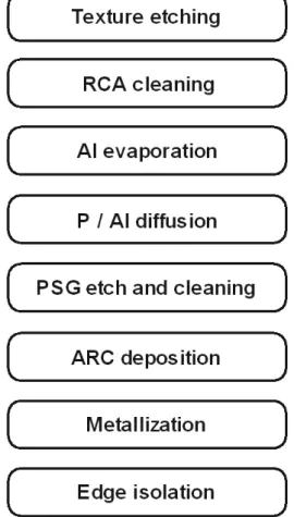
The manufacturing process for n+pn+ multicrystalline
silicon solar cells (without BSF) was implemented as follows: RCA cleaning, phosphorus diffusion based on POCl3 in a conventional quartz tube furnace, phosphorus
silicate glass (PSG) removal and RCA cleaning, TiO2 anti-relection coating (ARC) deposition by the electron
beam technique, screen printed metallization and laser edge isolation11. The RCA cleaning was performed using analytic grade chemicals and deionized water with electric
resistivity above 18 MΩ.cm. A metal grid with two busbars
was deposited on the front and rear face. The areas covered
by Ag paste (front face) and Ag/Al paste (rear face) were 8% and 53%, respectively. The metal coverage on the rear
face was optimized by solar cell simulation. The complete process included the solar cell surface texturing. The
manufacturing process is illustrated in Figure 1.
Aluminum deposition by e-beam evaporation was
introduced to the BSF solar cell (n+pp+) manufacturing process. The single step diffusion of phosphorus and
aluminum was developed using a conventional quartz tube furnace. This process was based on results obtained in
Si-Cz wafers12.
Silicon oxide growth is required to form the BSF in
the manufacture of solar cells with diffusion of aluminum
deposited by evaporation. Photoresist is deposited on one
surface and silicon oxide removal is performed on the other surface. Thus, phosphorus diffusion occurs only in the front
face. Following the oxide etching in chemical solution, the aluminum on the back surface is evaporated and diffused11,13.
A manufacturing process was developed to obtain n+pp+ Si-Mc solar cell and avoid oxidation, deposition of photoresist, and silicon oxide etching. The process was carried out with single-step thermal diffusion of phosphorus and aluminum. As a result, the production cost was reduced.
The process incorporated the following steps (see Figure 2): surface texturing using acidic solution, RCA cleaning, Al evaporation, single step Al and P diffusion, phosphorus silicate glass removal, RCA cleaning, TiO2 anti-relection coating deposition, screen printed metallization, iring of
metallization pastes, and laser edge isolation.
The thickness of evaporated aluminum in n+pp+ solar
cells was 2 μm and the thickness of TiO2 anti-relection coating was 68 nm. The Ag paste covered an area of 9% on the front face. The metallization paste iring was
implemented using a belt furnace, with temperature set at
870 °C and belt speed at 190 cm/min.
After the solar cells were processed, they were evaluated by measuring the electric current density versus applied
voltage (J-V) characteristic. Measurements were carried
out following the international standard: irradiance of 1000 W/m2 with spectrum AM 1.5G and cell temperature
of 25 °C. The standard solar cell was calibrated at the
Fraunhofer Institut für Solare Energiesysteme, Germany. The solar cells were also characterized by minority carrier
diffusion length and quantum eficiency. Experimental
results were also analyzed by simulating solar cells using
the PC-1D software.
3. Results and Discussion
3.1.
n
+pn
+solar cells with and without texturing
The manufacturing process for solar cells without BSF and no texturing lead to an eficiency of 12.3%. The cell presented the short-circuit density (JSC) of 29 mA/cm2, open
circuit voltage (VOC) of 572 mV and ill factor (FF) of 0.74.
These results were achieved with phosphorus diffusion at
875 °C, which resulted in the 30 Ω/□ sheet resistance. The
temperature of 860 °C was used for metallization paste iring. Figure 3 shows the comparison between n+pn+ solar
cell J-V curves with and without surface texturing. If the process included the texturing step, the maximum eficiency achieved was 13.8%, which is 1.5% (absolute) higher than the eficiency of the solar cell without texturing. The
electrical parameters of the solar cell with texturing were:
JSC = 29.3 mA/cm2, V
OC = 595 mV and FF = 0.79. Texturing
etch increased the ill factor and VOC, mainly. The positive results might have been obtained due to the improvement in the contact between metal and semiconductor. Texturing improved the JSC slightly. The increase in JSC was associated
with the reduction of relection in the front surface. The average relectance was reduced from 35% to 23% with the implementation of the texturing etch. Following the deposition of TiO2 anti-relection coating, the average relectance decreased to 6.4% for samples with texturing, and to 7.5% for samples without texturing etch. In this process, phosphorus diffusion was also carried out at 875 °C and the sheet resistance of approximately 35 Ω/□was obtained.
Metallization paste iring was performed at 870 °C.
3.2.
n
+pp
+solar cells
The experimental optimization of the manufacturing
process of solar cells with BSF showed that the best result was obtained with diffusion of both dopants at 875 °C,
and with aluminum diffusion for 90 minutes. The sheet resistance in the n+ region was 64 Ω/□.
The efficiency for n+pp+ solar cells was 14.1%.
Figure 4 shows the J-V characteristic obtained under
standard measuring conditions. The parameters were JSC = 30.2 mA/cm2, V
OC = 592 mV and FF = 0.78.
Figure 2. n+pp+ silicon solar cell manufacturing process.
Figure 4. Electrical characteristic of the n+pp+ solar cell at standard
conditions.
Figure 3. Electrical characteristics at standard conditions of the n+pn+ solar cells with and without texturing etching in acidic
presented in Table 1. The thickness of Si wafers was varied to evaluate solar cells with and without BSF. The relectance of the TiO2 anti-relection coating was considered in the simulation. The solar cells without BSF were simulated
using n+p structure because the rear metal grid perforated the n+ region. The simulated results are presented in the Table 2.
The 240 μm thick Si-Mc solar cell showed a 1.4% (absolute) increase in eficiency for the device with BSF in comparison with the solar cell without BSF. This thickness is similar to that of the solar cells developed and the improvement in the eficiency is higher than the value of 0.3% (absolute) obtained with the manufactured solar cells. For the devices with BSF, the main difference between experimental and simulated results was in VOC. This result,
in combination with a slight difference in the ill factor, was associated with the low experimental eficiency. The difference between experimental and simulated eficiency
may be related to the single step diffusion for the two
dopants (which may affect the effectiveness of BSF), the different base resistivity or the inferior quality of the Si-Mc
conditions.
The BSF solar cell eficiency was modestly affected by the reduction of the thickness from 400 μm to 100 μm. The VOC increased slightly, and the JSC decreased. However, for
devices without BSF, the eficiency decreased as function of the reduction in thickness. In these cells, JSC decreased.
Thus the result is similar to the result for the cells with BSF, though there was a decrease in VOC.
3.3.2. Analysis of minority carrier diffusion length
and quantum eficiency
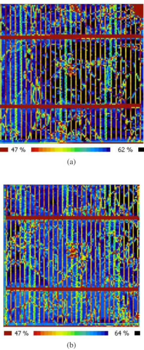
The minority carrier diffusion length (LD) of the
n+pn+ and n+pp+ solar cells was also compared, as shown
in Figure 5. The result was obtained from the light beam induced current (LBIC) measurements carried out with WT1000-PV equipment (Semilab). The average diffusion length for 132 μm BSF solar cells was 20% greater than the average value measured in the solar cells without BSF (LD = 112 μm). This result indicates the low effectiveness of the BSF. For both types of solar cells, the LD was inferior
to the thickness of the cell of 240 μm. In this case, the BSF had little effect on the dark saturation current. If the minority carrier lifetime is high (i.e., the minority carrier diffusion length is greater than the thickness of the solar cell), the minority carriers reach the BSF easily and the dark saturation current becomes a function of the rear
recombination velocity2.
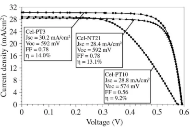
The external quantum efficiency (EQE) of three solar cells was also measured: Cel-PT3 with η = 14.0%,
Cel-PT10 with η = 9.2% (both with BSF) and Cel-NT21
with η = 13.1% (without BSF). The comparison of the
two-dimensional distribution of the EQE obtained with a laser radiation wavelength of 973 nm is shown in Figure 6.
The average EQEs of the solar cells Cel-PT3, Cel-PT10 and Cel-NT21 were 54.4%, 55.8% and 51.5%, respectively. The BSF did not signiicantly affect the EQE. The solar cells Cel-PT3 and Cel-PT10 showed only slightly higher EQE values when compared with cell Cel-NT21 (without Al-BSF). This result conirms the low effectiveness of the BSF obtained with the single thermal step for the diffusion of phosphorus and aluminum. The J-V curve shows that the solar cell Cel-PT10 had a high series resistance. The
resistance has a negative effect on the fill factor and,
consequently, reduces the VOC, as shown in Figure 7. This inding may be related to the formation of aluminum oxide (Al2O3) during the diffusion of phosphorus, which, in turn,
damages the formation of the metal-semiconductor contact on the rear face.
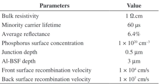
Table 1. Parameters for simulation of n+pn+ and n+pp+ solar cells.
Parameters Value
Bulk resistivity 1 Ω.cm
Minority carrier lifetime 60 μs
Average relectance 6.4% Phosphorus surface concentration 1 × 1020 cm–3
Junction depth 0.5 µm
Al-BSF depth 3 µm
Front surface recombination velocity 1 × 104 cm/s
Back surface recombination velocity 1 × 107 cm/s
Table 2. Electrical parameters of the solar cells simulated as a function of thickness of the silicon multicrystalline wafer.
Thickness (µm)
JSC (mA/cm2)
VOC (mV)
FF η (%)
n+pn+
(without BSF)
100 26.4 597.6 0.79 12.5 200 27.9 614.1 0.79 13.6 240 28.3 617.8 0.79 13.9
400 29.0 626.1 0.79 14.4
n+pp+
(BSF)
3.3.3. Analysis of the inluence of base resistivity
Base resistivity is a parameter that influences the performance of solar cells with and without BSF in
different ways. The substrate used in this study had a
resistivity between 0.5-2.0 Ω.cm. In low resistivity materials (<1 Ω.cm), BSF has less effect in the eficiency of the solar cell. BSF is recommended for substrates with greater resistivity. It is also recommended if the wafer thickness is
lower than the minority carrier diffusion length.
The solar cell simulations were carried out using a
thickness of 240 μm and the parameters in Table 1. The base resistivity was varied according to the igures in Table 3. Both kinds of solar cells showed an increase in eficiency
with the reduction of base resistivity. If the resistivity is
increased from 0.5 to 2 Ω.cm, the solar cells without BSF
Figure 5. Two-dimensional distribution of the minority carrier diffusion length in (a) n+pn+ and (b) n+pp+ solar cells.
(a)
(b)
Figure 6. Two-dimensional distribution of the EQE of the solar cells (a) Cel-PT3 (n+pp+), (b) Cel-PT10 (n+pp+) and c) Cel-NT21 (n+pn+).
(c) (a)
showed a reduction of 1.1% (absolute) in eficiency. This
result is superior to the 0.3% reduction for solar cells with
BSF. There was a slight decrease in JSC with the reduction in
the base resistivity. However, the ill factor and VOC increased for both solar cells.
The base resistivity of 10 Ω.cm resulted in the eficiency of 14.1%, which is equivalent to the experimental result for BSF devices (see Table 3). Base resistivity explains also
the difference between experimental results of solar cells
with and without BSF. The VOC of 604 mV obtained in the
simulation was the closest value to the experimental value
of 592 mV.
to 1.4%. Finally, the VOC parameter presented the biggest difference between experimental and simulated values.
For solar cells without BSF, the experimental eficiency was similar to the simulated eficiency, but there were differences in VOC and JSC. The ill factor presented similar
experimental and simulated results for both kinds of solar cells. The reduction in the thickness of the substrate caused a modest reduction in the eficiency of BSF solar cells, however affected the solar cells without BSF more signiicantly.
The minority carrier diffusion length was only 20%
higher for BSF cells. This result shows that the single step
thermal diffusion of phosphorus and aluminum produces
a less-effective BSF. The eficiency of some BSF solar
cells was limited by series resistance. This series resistance possibly results from the formation of aluminum oxide
(Al2O3) during the diffusion of phosphorus. Consequently, the back metal-semiconductor contact may be affected.
Simulations showed that the eficiency of solar cells with and without BSF increases with the reduction of base resistivity. The eficiency of the simulated BSF solar cells with 10 Ω.cm base resistivity was equivalent to the
experimental result.
In conclusion, base resistivity may be associated with the fact that there was a small difference of 0.3%
(absolute) between the efficiency of devices with and without BSF. Another factor that inluenced the result was the low effectiveness of the BSF formed during single step
phosphorus and aluminum diffusion.
Acknowledgments
The authors gratefully acknowledge the financial support of the State Electric Energy Distribution Company (CEEE-D), contract CEEE/D2009-9928171.
Table 3. Electrical parameters for n+pn+ and n+pp+ solar cells with
240 μm thickness as a function of the base resistivity of the Si-Mc substrate.
Resistivity (Ω.cm)
JSC
(mA/cm2)
VOC
(mV)
FF η
(%)
n+pn+
0.5 28.2 636.8 0.80 14.4 1 28.3 617.8 0.79 13.9 2 28.3 597.9 0.79 13.3 10 28.5 551.7 0.77 12.1
n+pp+
0.5 29.6 648.8 0.80 15.3 1 30.0 638.9 0.80 15.3 2 30.3 627.8 0.79 15.0 10 30.5 604.1 0.76 14.1
References
1. Hering G. Enter the dragon. Photon International. 2012:132-160.
2. Luque A and Hegedus S. Handbook of Photovoltaic Science and
Engineering. West Sussex: John Wiley&Sons; 2003. 1115 p.
http://dx.doi.org/10.1002/0470014008
3. Ebong A, Cooper IB, Rounsaville A, Rohatgi A, Borland W, Mikeska K et al. Overcoming the technological challenges of contacting homogeneous high sheet resistance emitters (HHSE). In: Proceedings of the 26th European Photovoltaic
Solar Energy Conference and Exhibition; 2011; Hamburg,
Germany. WIP; 2011. p. 1747-1749.
4. Fath P, Keller S, Winter P, Joss W and Herbst W. Status and perspective of crystalline silicon solar cell production.
In: Proceedings of the 34th IEEE Photovoltaic Specialists
Conference (PVSC); 2009; Philadelphia, USA. IEEE; 2009.
p. 2471-2476. http://dx.doi.org/10.1109/PVSC.2009.5411274 5. Green MA, Emery K, Hishikawa Y, Warta W and Dunlop
Ewan D. Solar cell eficiency tables (Version 41). Progress
in Photovoltaics: Research and Applications. 2013; 21:1-11.
http://dx.doi.org/10.1002/pip.2352
6. Green MA, Zhao J, Wang A and Wenham SR. Very high eficiency silicon solar cells – science and technology. IEEE
Transactions on Electron Devices. 1999; 46(10):1940-1947.
http://dx.doi.org/10.1109/16.791982 Figure 7. Current density as a function of the voltage of the solar
7. Schultz O, Glunz SW and Willeke GP. Multicrystalline silicon solar cells exceeding 20% eficiency. Progress in Photovoltaics: Research and Applications. 2004; 12:553-558 http://dx.doi. org/10.1002/pip.583
8. Green MA, Emery K, Hishikawa Y and Warta W. Solar cell eficiency tables (version 37). Progress in Photovoltaics: Research and Applications. 2011; 19:84-92. http://dx.doi. org/10.1002/pip.1088
9. Niinobe D, Nishimura K, Matsuno S, Fujioka H, Katsura T, Okamoto T et al. Honeycomb structured multi-crystalline silicon solar cells with 18.6% efficiency via industrially applicable laser-process. In: Proceedings of the 23rd European
Photovoltaic Solar Energy Conference and Exhibition; 2008;
Valencia, Spain. WIP; 2008. p. 1824-1828.
10. Engelhart P, Zimmermann G, Klenke C, Wendt J, Kaden T, Junghänel M et al. R&D pilot-line production of multi-crystalline Si solar cells with top eficiencies exceeding 19%.
In: Proceedings of the 37th IEEE Photovoltaic Specialists
Conference (PVSC); 2011; Seattle, USA. IEEE; 2011. p.
1919-1923.
11. Moehlecke A and Zanesco I. Development of silicon solar cells and photovoltaic modules in Brazil: analysis of a pilot production. Materials Research, 2012; 15:581-588. http:// dx.doi.org/10.1590/S1516-14392012005000084
12. Zanesco I and Moehlecke A. Implementação de duas unidades geradoras de energia elétrica com módulos fotovoltaicos eficientes. Porto Alegre; 2010. 387 p. Relatório técnico, MME 008/2005.
13. Moehlecke A and Zanesco I. Pilot production of n+pn+ and
n+pp+ silicon solar cells: eficiency x yield. In: Proceedings of
the 25th European Photovoltaic Solar Energy Conference and Exhibition and 5th World Conference on Photovoltaic Energy